 | –≠–ª–µ–∫—Ç—Ä–æ–Ω–Ω—ã–π –∫–æ–º–ø–æ–Ω–µ–Ω—Ç: OPA2111 | –°–∫–∞—á–∞—Ç—å:  PDF PDF  ZIP ZIP |

Dual Low Noise Precision
Difet
Æ
OPERATIONAL AMPLIFIER
FEATURES
q
LOW NOISE: 100% Tested, 8nV/
Hz max at
10kHz
q
LOW BIAS CURRENT: 4pA max
q
LOW OFFSET: 500
µ
V max
q
LOW DRIFT: 2.8
µ
V/
∞
C
q
HIGH OPEN-LOOP GAIN: 114dB min
q
HIGH COMMON-MODE REJECTION:
96dB min
APPLICATIONS
q
PRECISION INSTRUMENTATION
q
DATA ACQUISITION
q
TEST EQUIPMENT
q
PROFESSIONAL AUDIO EQUIPMENT
q
MEDICAL EQUIPMENT
q
DETECTOR ARRAYS
International Airport Industrial Park ∑ Mailing Address: PO Box 11400 ∑ Tucson, AZ 85734 ∑ Street Address: 6730 S. Tucson Blvd. ∑ Tucson, AZ 85706
Tel: (520) 746-1111 ∑ Twx: 910-952-1111 ∑ Cable: BBRCORP ∑ Telex: 066-6491 ∑ FAX: (520) 889-1510 ∑ Immediate Product Info: (800) 548-6132
BIFET
Æ
National Semiconductor Corp.,
Difet
Æ
Burr-Brown Corp.
Noise-Free
Cascode*
OPA2111 Simplified Circuit
(Each Amplifier)
8
4
Output
+V
CC
≠V
CC
≠In
+In
*Patented
OPA2111
Æ
DESCRIPTION
The OPA2111 is a high precision monolithic
dielectrically isolated FET (
Difet
) operational ampli-
fier. Outstanding performance characteristics allow its
use in the most critical instrumentation applications.
Noise, bias current, voltage offset, drift, open-loop
gain, common-mode rejection, and power supply re-
jection are superior to BIFET
Æ
amplifiers.
Very low bias current is obtained by dielectric isola-
tion with on-chip guarding.
Laser trimming of thin-film resistors gives very low
offset and drift. Extremely low noise is achieved with
patented circuit design techniques. A cascode design
allows high precision input specifications and reduced
susceptibility to flicker noise.
Standard dual op amp pin configuration allows up-
grading of existing designs to higher performance
levels.
© 1984 Burr-Brown Corporation
PDS-540E
Printed in U.S.A. October, 1993
Æ
OPA2111
2
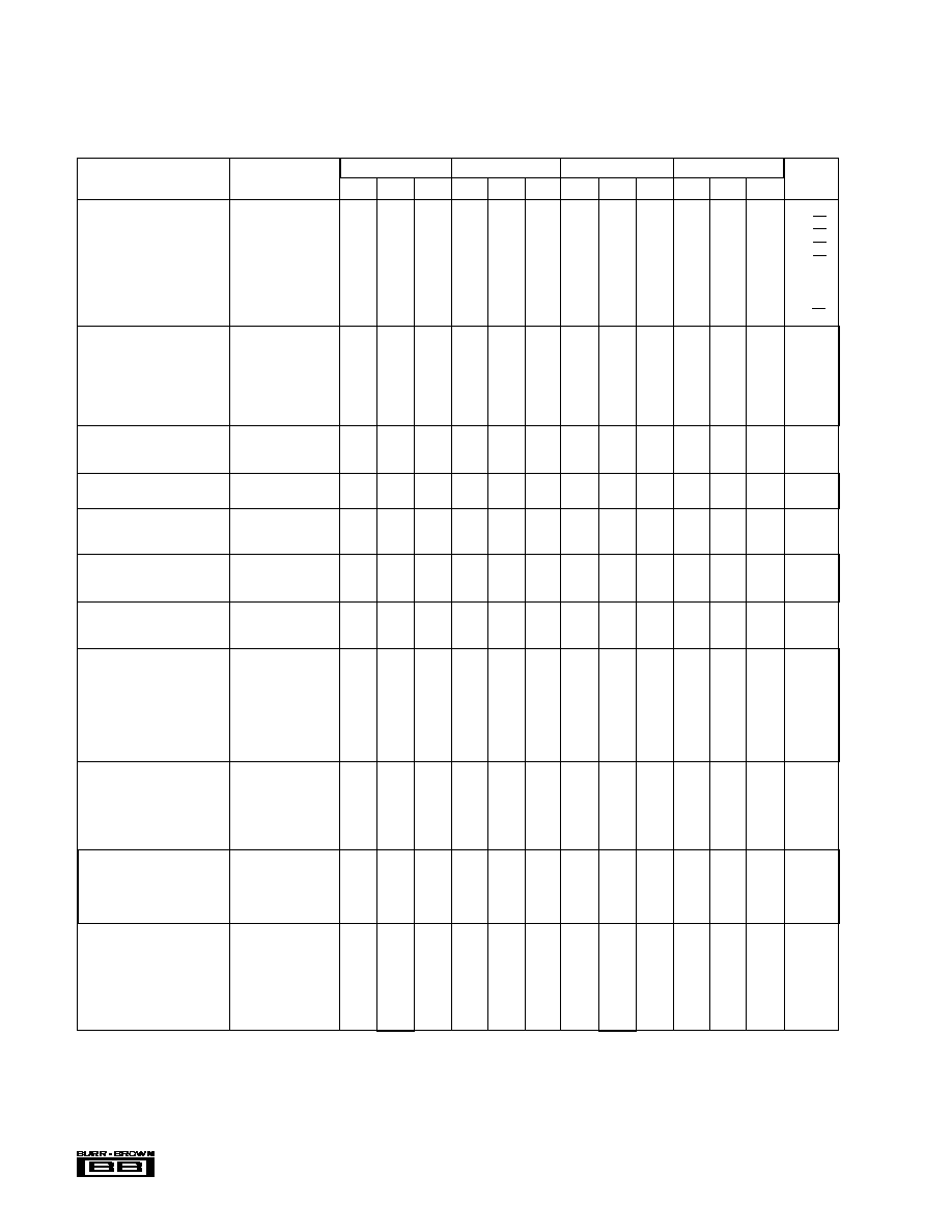
SPECIFICATIONS
ELECTRICAL
At V
CC
=
±
15VDC and T
A
= +25
∞
C unless otherwise noted
.
OPA2111AM
OPA2111BM
OPA2111SM
OPA2111KM, KP
PARAMETER
CONDITION
MIN
TYP
MAX
MIN
TYP
MAX
MIN
TYP
MAX
MIN
TYP
MAX
UNITS
INPUT NOISE
Voltage, f
O
= 10Hz
100% Tested
40
80
30
60
40
80
40
nV/
Hz
f
O
= 100Hz
100% Tested
15
40
11
30
15
40
15
nV/
Hz
f
O
= 1kHz
100% Tested
8
15
7
12
8
15
8
nV/
Hz
f
O
= 10kHz
(1)
6
8
6
8
6
8
6
nV/
Hz
f
B
= 10Hz to 10kHz
(1)
0.7
1.2
0.6
1
0.7
1.2
0.7
µ
Vrms
f
B
= 0.1Hz to 10Hz
(1)
1.6
3.3
1.2
2.5
1.6
3.3
1.6
µ
Vp-p
Current, f
B
= 0.1Hz to 10Hz
(1)
15
24
12
19
15
24
15
fAp-p
f
O
= 0.1Hz to 20kHz
(1)
0.8
1.3
0.6
1
0.8
1
0.8
fA/
Hz
OFFSET VOLTAGE
(2)
Input Offset Voltage
V
CM
= 0VDC
±
0.1
±
0.75
±
0.05
±
0.5
±
0.1
±
0.75
±
0.3
±
2
mV
Average Drift
T
A
= T
MIN
to T
MAX
±
2
±
6
±
0.5
±
2.8
±
2
±
6
±
8
±
15
µ
V/
∞
C
Match
±
1
±
0.5
2
2
µ
V/
∞
C
Supply Rejection
90
110
96
110
90
110
86
110
dB
±
3
±
31
±
3
±
16
±
3
±
31
±
3
±
50
µ
V/V
Channel Separation
100Hz, R
L
= 2k
136
136
136
136
dB
BIAS CURRENT
(2)
Input Bias Current
V
CM
= 0VDC
±
2
±
8
±
1.2
±
4
±
2
±
8
±
3
±
15
pA
Match
±
1
±
0.5
±
1
2
pA
OFFSET CURRENT
(2)
Input Offset Current
V
CM
= 0VDC
±
1.2
±
6
±
0.6
±
3
±
1.2
±
6
±
3
±
12
pA
IMPEDANCE
Differential
10
13
|| 1
10
13
|| 1
10
13
|| 1
10
13
|| 1
|| pF
Common-Mode
10
14
|| 3
10
14
|| 3
10
14
|| 3
10
14
|| 3
|| pF
VOLTAGE RANGE
Common-Mode Input Range
±
10
±
11
±
10
±
11
±
10
±
11
±
10
±
11
V
Common-Mode Rejection
V
IN
=
±
10VDC
90
110
96
110
90
110
82
110
dB
OPEN-LOOP GAIN, DC
Open-Loop Voltage Gain
R
L
2k
110
125
114
125
110
125
106
125
dB
Match
3
2
3
3
dB
FREQUENCY RESPONSE
Unity Gain, Small Signal
2
2
2
2
MHz
Full Power Response
20Vp-p, R
L
= 2k
16
32
16
32
16
32
32
kHz
Slew Rate
V
O
=
±
10V, R
L
= 2k
1
2
1
2
1
2
2
V/
µ
s
Settling Time, 0.1%
Gain = ≠1, R
L
= 2k
6
6
6
6
µ
s
0.01%
10V Step
10
10
10
10
µ
s
Overload Recovery,
50% Overdrive
(3)
Gain = ≠1
5
5
5
5
µ
s
RATED OUTPUT
Voltage Output
R
L
= 2k
±
10
±
11
±
10
±
11
±
10
±
11
±
10
±
11
V
Current Output
V
O
=
±
10VDC
±
5
±
10
±
5
±
10
±
5
±
10
±
5
±
10
mA
Output Resistance
DC, Open-Loop
100
100
100
100
Load Capacitance Stability
Gain = +1
1000
1000
1000
1000
pF
Short Circuit Current
10
40
10
40
10
40
10
40
mA
POWER SUPPLY
Rated Voltage
±
15
±
15
±
15
±
15
VDC
Voltage Range, Derated
Performance
±
5
±
18
±
5
±
18
±
5
±
18
±
5
±
18
VDC
Current, Quiescent
I
O
= 0mADC
5
7
5
7
5
7
5
9
mA
TEMPERATURE RANGE
Specification
Ambient Temp.
≠25
+85
≠25
+85
≠55
+125
0
+70
∞
C
Operating "M" Package
Ambient Temp.
≠55
+125
≠55
+125
≠55
+125
≠55
+125
∞
C
"P" Package
≠40
+85
∞
C
Storage "M" Package
Ambient Temp.
≠65
+150
≠65
+150
≠65
+150
≠65
+150
∞
C
"P" Package
≠40
+85
∞
C
Junction-Ambient
200
200
200
200
(4)
∞
C/W
NOTES: (1) Sample tested--this parameter is guaranteed. (2) Offset voltage, offset current, and bias current are measured with the units fully warmed up. (3) Overload
recovery is defined as the time required for the output to return from saturation to linear operation following the removal of a 50% input overdrive. (4) Typical
J-A
=
150
∞
C/W for plastic DIP.
Æ
OPA2111
3
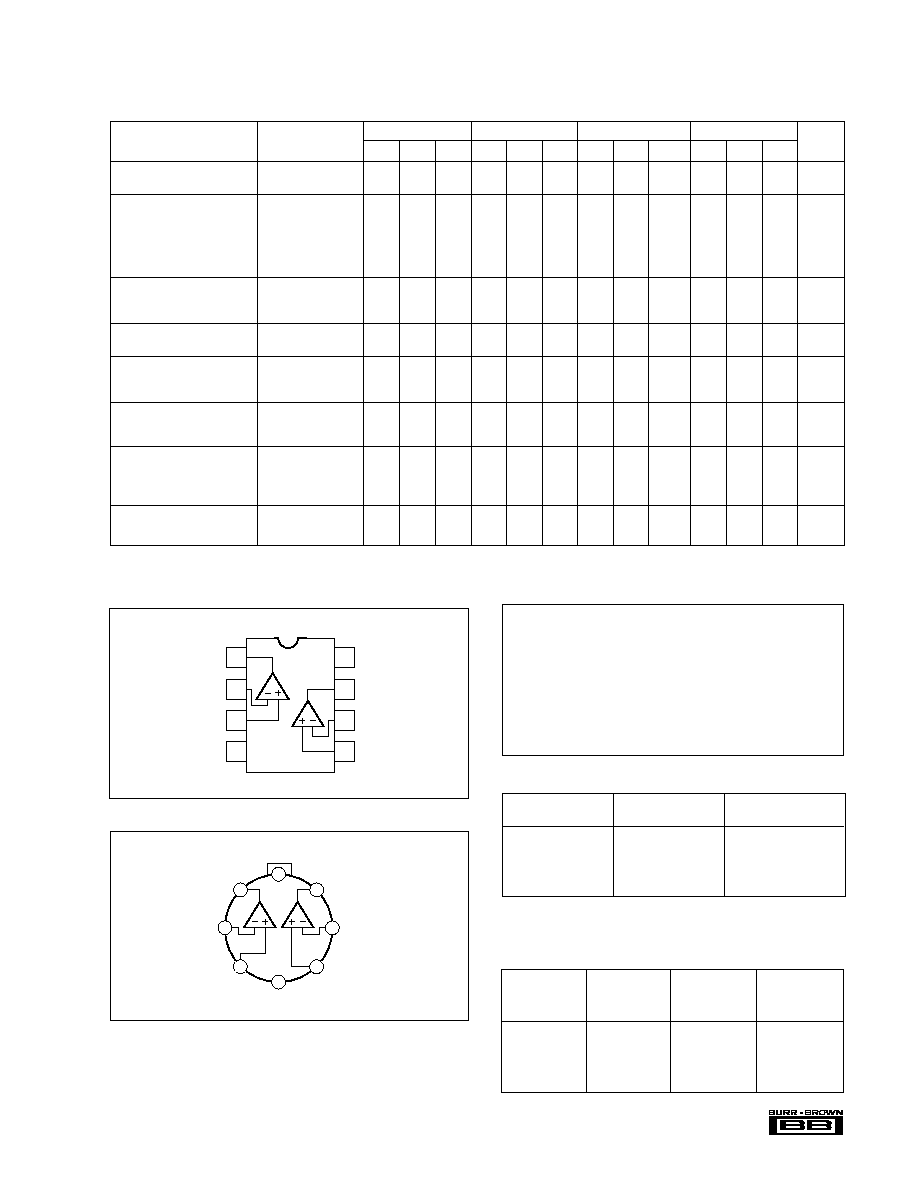
ELECTRICAL (FULL TEMPERATURE RANGE SPECIFICATIONS)
At V
CC
=
±
15VDC and T
A
= T
MIN
to T
MAX
unless otherwise noted.
OPA2111AM
OPA2111BM
OPA2111SM
OPA2111KM, KP
PARAMETER
CONDITION
MIN
TYP
MAX
MIN
TYP
MAX
MIN
TYP
MAX
MIN
TYP
MAX
UNITS
TEMPERATURE RANGE
Specification Range
Ambient Temp.
≠25
+85
≠25
+85
≠55
+125
0
+70
∞
C
INPUT OFFSET VOLTAGE
(1)
Input Offset Voltage
V
CM
= 0VDC
±
0.22
±
1.2
±
0.08
±
0.75
±
0.3
±
1.5
±
0.9
±
5
mV
Average Drift
±
2
±
6
±
0.5
±
2.8
±
2
±
6
±
8
±
15
µ
V/
∞
C
Match
1
0.5
2
2
µ
V/
∞
C
Supply Rejection
86
100
90
100
86
100
82
100
dB
±
10
±
50
±
10
±
32
±
10
±
50
±
10
±
80
µ
V/V
BIAS CURRENT
(1)
Input Bias Current
V
CM
= 0VDC
±
125
±
1nA
±
75
±
500
±
2nA
±
16.3nA
±
125
±
500
pA
Match
60
30
1nA
pA
OFFSET CURRENT
(1)
Input Offset Current
V
CM
= 0VDC
±
75
±
750
±
38
±
375
±
1.3nA
±
12nA
±
75
±
375
pA
VOLTAGE RANGE
Common-Mode Input Range
±
10
±
11
±
10
±
11
±
10
±
11
±
10
±
11
V
Common-Mode Rejection
V
IN
=
±
10VDC
86
100
90
100
86
100
80
100
dB
OPEN-LOOP GAIN, DC
Open-Loop Voltage Gain
R
L
2k
106
120
110
120
106
120
100
120
dB
Match
5
3
5
5
dB
RATED OUTPUT
Voltage Output
R
L
= 2k
±
10.5
±
11
±
10.5
±
11
±
10.5
±
11
±
10.5
±
11
V
Current Output
V
O
=
±
10VDC
±
5
±
10
±
5
±
10
±
5
±
10
±
5
±
10
mA
Short Circuit Current
V
O
= 0VDC
10
40
10
40
10
40
10
40
mA
POWER SUPPLY
Current, Quiescent
I
O
= 0mADC
5
8
5
8
5
8
5
10
mA
NOTES: (1) Offset voltage, offset current, and bias current are measured with the units fully warmed up.
CONNECTION DIAGRAMS
Top View
DIP
A
B
1
2
3
4
8
7
6
5
Out A
≠In A
+In A
≠V
CC
+V
CC
Out B
≠In B
+In B
Top View
TO-99
8
1
2
7
6
5
3
4
Out A
+In B
≠In B
Out B
≠V
CC
≠In A
+In A
A
B
+V
CC
and Case
ABSOLUTE MAXIMUM RATINGS
Supply ...........................................................................................
±
18VDC
Internal Power Dissipation (T
J
+175
∞
C) .................................... 500mW
Differential Input Voltage ............................................................ Total V
CC
Input Voltage Range ..........................................................................
±
V
CC
Storage Temperature Range: "M" Package .................. ≠65
∞
C to +150
∞
C
"P" Package .................... ≠40
∞
C to +85
∞
C
Operating Temperature Range: "M" Package ............... ≠55
∞
C to +125
∞
C
"P" Package ................. ≠40
∞
C to +85
∞
C
Lead Temperature (soldering, 10s) ............................................... +300
∞
C
Output Short Circuit to Ground (+25
∞
C) ................................. Continuous
Junction Temperature .................................................................... +175
∞
C
PACKAGE INFORMATION
PACKAGE DRAWING
MODEL
PACKAGE
NUMBER
(1)
OPA2111AM
TO-99
001
OPA2111BM
TO-99
001
OPA2111KM
TO-99
001
OPA2111SM
TO-99
001
OPA2111KP
8-Pin Plastic DIP
006
NOTE: (1) For detailed drawing and dimension table, please see end of data
sheet, or Appendix D of Burr-Brown IC Data Book.
OFFSET
TEMPERATURE
VOLTAGE,
MODEL
PACKAGE
RANGE
max (mV)
1≠24
OPA2111AM
TO-99
≠25
∞
C to +85
∞
C
±
0.75
$12.50
OPA2111BM
TO-99
≠25
∞
C to +85
∞
C
±
0.5
21.60
OPA2111KM
TO-99
0
∞
C to +70
∞
C
±
2
25.55
OPA2111SM
TO-99
≠55
∞
C to +125
∞
C
±
0.75
OPA2111KP
8-Pin Plastic DIP
0
∞
C to +70
∞
C
±
2
ORDERING INFORMATION
Æ
OPA2111
4
PAD
FUNCTION
1
Out A
2
≠In A
3
+In A
4
≠V
S
5
+In B
6
≠In B
7
Out B
8
+V
S
NC
No Connection
Substrate Bias: No Connection
DICE INFORMATION
MECHANICAL INFORMATION
MILS (0.001")
MILLIMETERS
Die Size
138 x 84
±
5
3.51 x 2.13
±
0.13
Die Thickness
20
±
3
0.51
±
0.08
Min. Pad Size
4 x 4
0.10 x 0.10
Backing
None
Transistor Count
102
OPA2111AD DIE TOPOGRAPHY
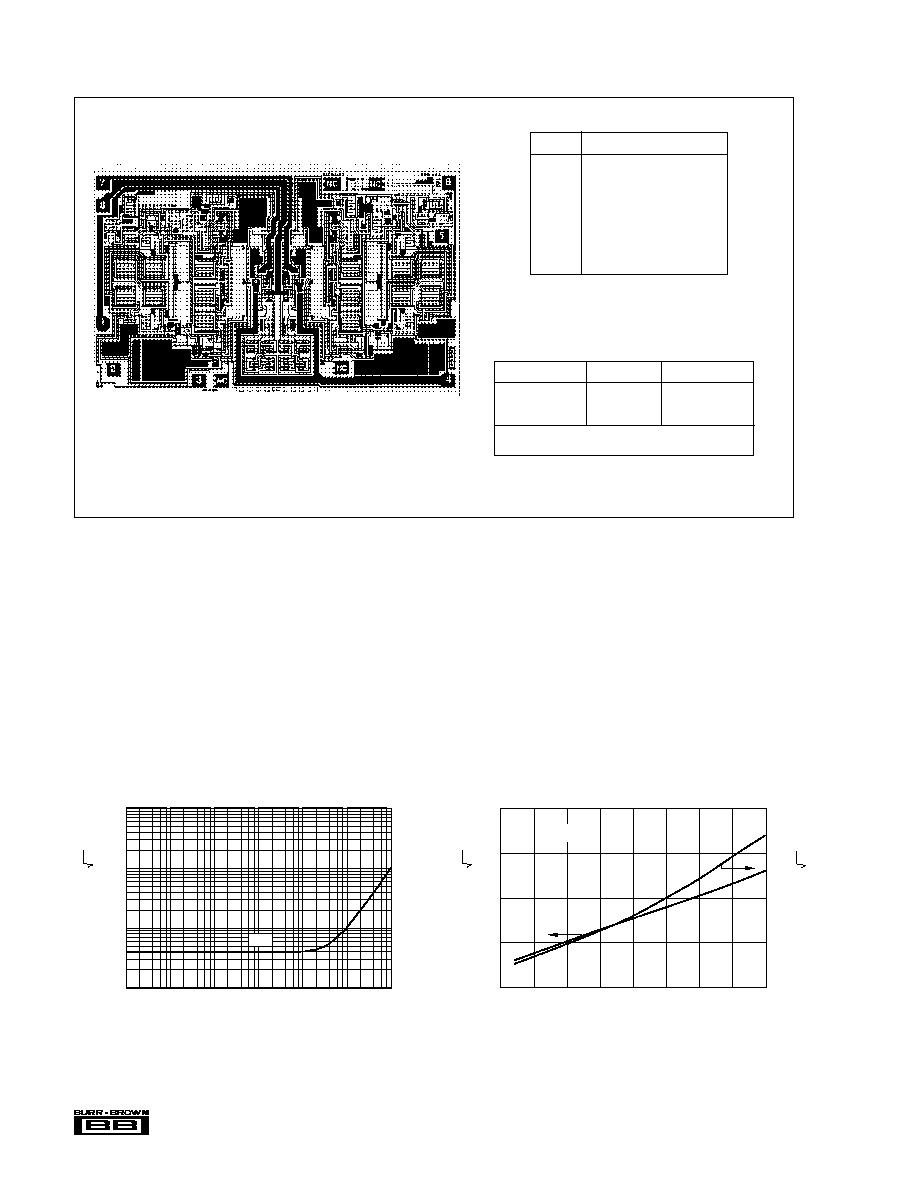
TYPICAL PERFORMANCE CURVES
T
A
= +25
∞
C, and V
CC
=
±
15VDC unless otherwise noted.
INPUT CURRENT NOISE SPECTRAL DENSITY
1k
Frequency (Hz)
100
10
1
10k
100k
1M
100
10
1
Current Noise (fA/
Hz)
BM
0.1
VOLTAGE AND CURRENT NOISE SPECTRAL
DENSITY vs TEMPERATURE
12
10
8
6
≠50
≠25
0
25
50
75
100
125
Temperature (∞C)
≠75
Voltage Noise (nV/ Hz)
100
10
1
0.1
0.01
Current Noise (fA/ Hz)
4
f
O
= 1kHz
Æ
OPA2111
5
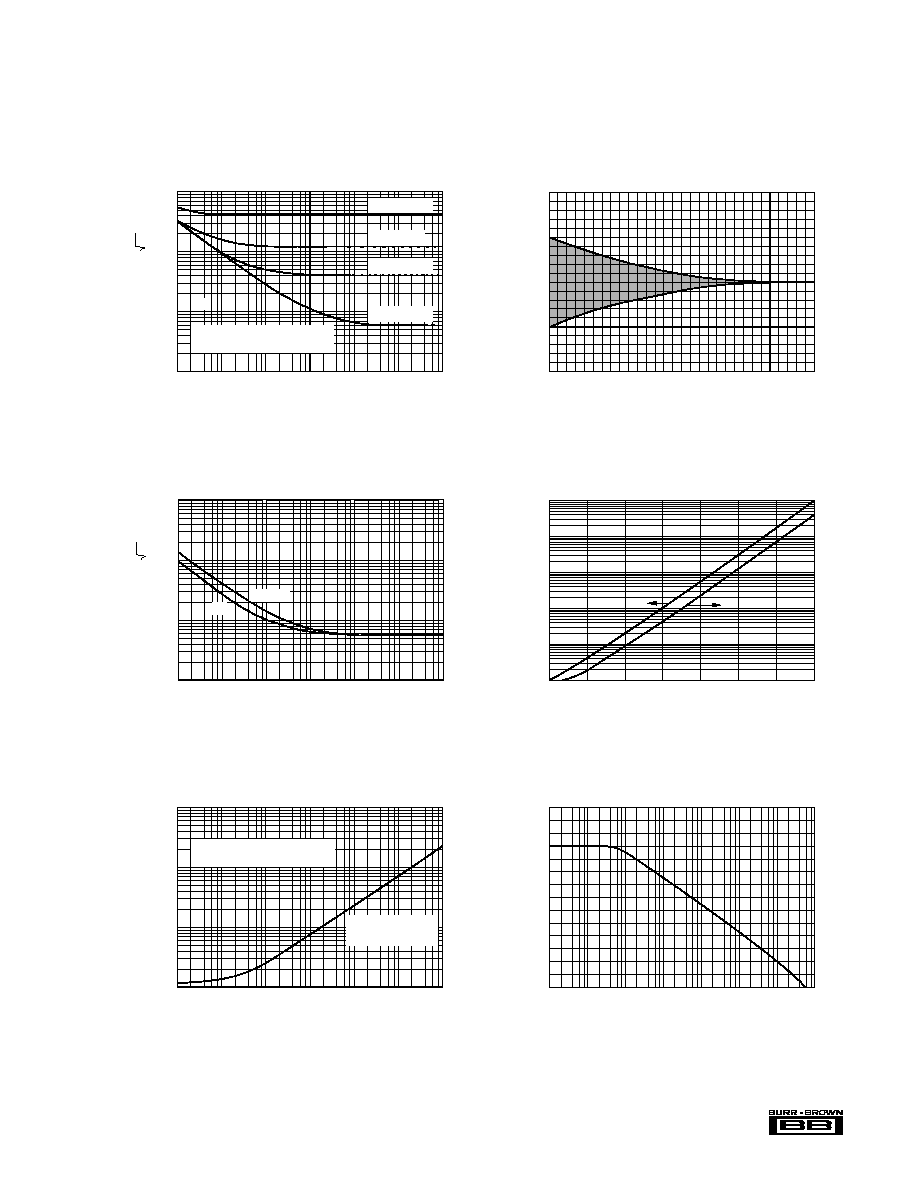
TYPICAL PERFORMANCE CURVES
(CONT)
T
A
= +25
∞
C, and V
CC
=
±
15VDC unless otherwise noted.
TOTAL
(1)
INPUT VOLTAGE NOISE SPECTRAL
DENSITY vs SOURCE RESISTANCE
100
Frequency (Hz)
1k
10k
100k
10
1
0.1
1k
100
10
Voltage Noise (nV/ Hz)
BM
NOTE: (1) Includes contribution
from source resistance.
1
R
S
= 10M
R
S
= 1M
R
S
= 100k
R
S
= 100
INPUT OFFSET VOLTAGE WARM-UP DRIFT
40
20
0
≠20
Time From Power Turn-On (Minutes)
Offset Voltage Change (µV)
0
1
2
3
4
5
6
≠40
INPUT VOLTAGE NOISE SPECTRAL DENSITY
1k
Frequency (Hz)
10k
100k
1M
100
10
1
1k
100
10
Voltage Noise (nV/ Hz)
BM
AM, SM
1
BIAS AND OFFSET CURRENT
vs TEMPERATURE
≠50
Ambient Temperature (∞C)
≠25
0
25
50
75
100
125
1k
100
10
1
0.1
Bias Current (pA)
1k
100
10
1
0.1
Offset Current (pA)
0.01
0.01
TOTAL
(1)
INPUT VOLTAGE NOISE (PEAK-TO-PEAK)
vs SOURCE RESISTANCE
10
1k
100
10
Voltage Noise (µVp-p)
NOTE: (1) Includes contribution
from source resistance.
4
Source Resistance (
)
10
5
10
6
10
7
10
8
10
9
10
10
1
BM
f
B
= 0.1Hz to 10Hz
POWER SUPPLY REJECTION
vs FREQUENCY
1
Frequency (Hz)
10
100
1k
10k
100k
1M
10M
Power Supply Rejection (dB)
140
120
100
80
60
40
20
0
Æ
OPA2111
6
TYPICAL PERFORMANCE CURVES
(CONT)
T
A
= +25
∞
C, and V
CC
=
±
15VDC unless otherwise noted.
TOTAL INPUT VOLTAGE NOISE SPECTRAL DENSITY
AT 1kHz vs SOURCE RESISTANCE
1k
100
10
Voltage Noise, E
O
(nV/ Hz)
100
1k
10k
100k
1M
10M
100M
Resistor Noise Only
OPA2111 +
Resistor
1
E
O
R
S
BM
Source Resistance (
)
COMMON-MODE REJECTION
vs INPUT COMMON-MODE VOLTAGE
≠15
Common-Mode Voltage (V)
≠10
≠5
0
5
10
15
Common-Mode Rejection (dB)
120
110
100
90
80
70
INPUT OFFSET VOLTAGE CHANGE
DUE TO THERMAL SHOCK
150
75
0
≠75
Time From Thermal Shock (Minutes)
Offset Voltage Change (µV)
≠1
0
1
2
3
4
5
25∞C
85∞C
BM
AM
Air Environment
≠150
T
A
= 25∞C to T
A
= 85∞C
GAIN-BANDWIDTH AND SLEW RATE
vs TEMPERATURE
≠50
≠25
0
25
50
75
100
125
Ambient Temperature (∞C)
Gain Bandwidth (MHz)
≠75
4
3
2
1
0
Slew Rate (V/µs)
4
3
2
1
0
10
1
0.1
BIAS AND OFFSET CURRENT
vs INPUT COMMON-MODE VOLTAGE
≠15
≠10
≠5
0
5
10
15
Bias Current (pA)
Offset Current (pA)
Common-Mode Voltage (V)
Bias Current
Offset Current
0.01
0.01
10
1
0.1
OPEN-LOOP GAIN vs TEMPERATURE
140
130
120
110
≠50
≠25
0
25
50
75
100
125
Ambient Temperature (∞C)
Voltage Gain (dB)
≠75
100
Æ
OPA2111
7
TYPICAL PERFORMANCE CURVES
(CONT)
T
A
= +25
∞
C, V
CC
=
±
15VDC unless otherwise noted.
COMMON-MODE REJECTION
vs FREQUENCY
1
Frequency (Hz)
10
100
1k
10k
100k
1M
10M
Common-Mode Rejection (dB)
140
120
100
80
60
40
20
0
LARGE SIGNAL TRANSIENT RESPONSE
Time (µs)
0
50
15
0
≠15
Output Voltage (V)
25
OPEN-LOOP FREQUENCY RESPONSE
1
Frequency (Hz)
10
100
1k
10k
100k
1M
10M
Voltage Gain (dB)
140
120
100
80
60
40
20
Phase
Margin
65∞
≠45
≠90
≠135
Phase Shift (Degrees)
Gain
≠180
0
SETTLING TIME vs CLOSED-LOOP GAIN
1
Closed-Loop Gain (V/V)
10
100
1k
100
80
60
40
20
Settling Time (µs)
0.1%
0.01%
0
GAIN-BANDWIDTH AND SLEW RATE
vs SUPPLY VOLTAGE
Gain Bandwidth (MHz)
0
3
2
1
Slew Rate (V/µs)
3
2
1
5
10
15
20
Supply Voltage (±V
CC
)
0
0
CHANNEL SEPARATION vs FREQUENCY
10
Frequency (Hz)
100
10k
100k
150
140
130
120
110
Channel Separation (dB)
R
L
=
100
1k
R
L
= 2k
R
L
= 560
Æ
OPA2111
8
TYPICAL PERFORMANCE CURVES
(CONT)
T
A
= +25
∞
C, V
CC
=
±
15VDC unless otherwise noted.
APPLICATIONS INFORMATION
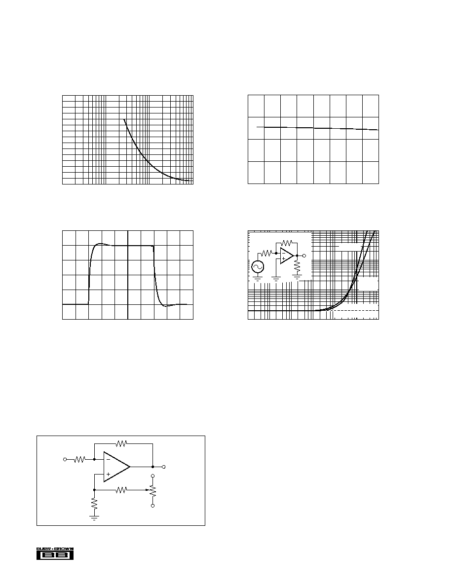
OFFSET VOLTAGE ADJUSTMENT
The OPA2111 offset voltage is laser-trimmed and will
require no further trim for most applications.
Offset voltage can be trimmed by summing (see Figure 1).
With this trim method there will be no degradation of input
offset drift.
INPUT PROTECTION
Conventional monolithic FET operational amplifiers require
external current-limiting resistors to protect their inputs
against destructive currents that can flow when input FET
gate-to-substrate isolation diodes are forward-biased. Most
BIFET amplifiers can be destroyed by the loss of ≠V
CC
.
Because of its dielectric isolation, no special protection is
needed on the OPA2111. Of course, the differential and
common-mode voltage limits should be observed. Static
damage can cause subtle changes in amplifier input charac-
teristics without necessarily destroying the device. In preci-
sion operational amplifiers (both bipolar and FET types),
this may cause a noticeable degradation of offset voltage and
drift.
Static protection is recommended when handling any preci-
sion IC operational amplifier.
FIGURE 1. Offset Voltage Trim.
MAXIMUM UNDISTORTED OUTPUT
VOLTAGE vs FREQUENCY
100k
Frequency (Hz)
1k
10k
1M
30
20
10
Output Voltage (Vp-p)
0
SUPPLY CURRENT vs TEMPERATURE
8
6
4
2
≠50
≠25
0
25
50
75
100
125
Ambient Temperature (∞C)
Supply Current (mA)
≠75
0
SMALL SIGNAL TRANSIENT RESPONSE
1
Time (µs)
0
5
Output Voltage (mV)
2
3
4
60
40
20
0
≠20
≠40
≠60
TOTAL HARMONIC DISTORTION
vs FREQUENCY
1
0.1
0.01
Total Harmonic Distortion (%)
0.1
1
10
100
1K
10K
100K
THD + Noise
Residual Test Limit
0.001
Frequency (Hz)
E
O
2k
10k
10k
E
O
= 7V
E
O
=
700mV
1/2 OPA2111
150k
Out
20
100k
≠15V
+15V
±2mV
OffsetTrim
In
Æ
OPA2111
9
APPLICATIONS CIRCUITS
Figures 5 through 13 are circuit diagrams of various appli-
cations for the OPA2111.
GUARDING AND SHIELDING
As in any situation where high impedances are involved,
careful shielding is required to reduce "hum" pickup in input
leads. If large feedback resistors are used, they should also
be shielded along with the external input circuitry.
Leakage currents across printed circuit boards can easily
exceed the bias current of the OPA2111. To avoid leakage
problems, it is recommended that the signal input lead of the
OPA2111 be wired to a Teflon standoff. If the OPA2111 is
to be soldered directly into a printed circuit board, utmost
care must be used in planning the board layout. A "guard"
pattern should completely surround the high impedance
input leads and should be connected to a low impedance
point which is at the signal input potential (see Figure 2).
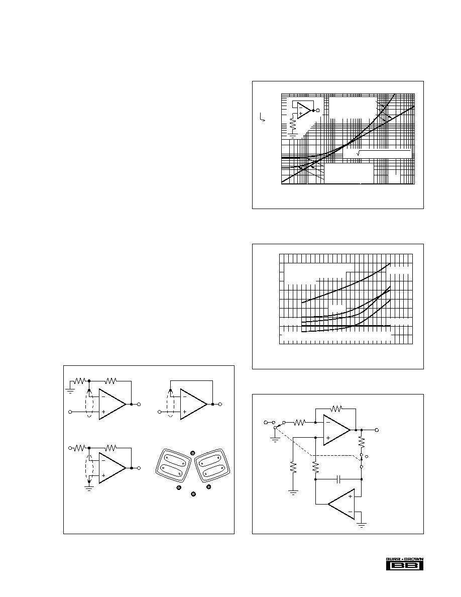
NOISE: FET vs BIPOLAR
Low noise circuit design requires careful analysis of all
noise sources. External noise sources can dominate in many
cases, so consider the effect of source resistance on overall
operational amplifier noise performance. At low source
impedances, the low voltage noise of a bipolar operational
amplifier is superior, but at higher impedances the high
current noise of a bipolar amplifier becomes a serious
liability. Above about 15k
the OPA2111 will have lower
total noise than an OP-27 (see Figure 3).
BIAS CURRENT CHANGE
vs COMMON-MODE VOLTAGE
The input bias currents of most popular BIFETÆ opera-
tional amplifiers are affected by common-mode voltage
(Figure 4). Higher input FET gate-to-drain voltage causes
leakage and ionization (bias) currents to increase. Due to its
cascode input stage, the extremely low bias current of the
OPA2111 is not compromised by common-mode voltage.
FIGURE 2. Connection of Input Guard.
FIGURE 5. Auto-Zero Amplifier.
FIGURE 3. Voltage Noise Spectral Density vs Source
Resistance.
FIGURE 4. Input Bias Currrent vs Common-Mode Voltage.
Out
10k
1M
1
2
3
7
6
5
1/2
OPA2111BM
100k
In
1µF
Polypropylene
100k
100
1/2
OPA2111BM
Operate
Zero
Gain = ≠100
V
OS
5µV
Drift
0.028µV/∞C
Zero Droop
2µV/s
Referred to Input
100
1k
10k
100k
1M
10M
1k
100
10
Voltage Noise Spectral Density (E
O
)
Typical at 1kHz (nV/
Hz)
BM
OP-27 + Resistor
OPA2111 + Resistor
Resistor Noise Only
OPA2111 + Resistor
Resistor Noise Only
OP-27 + Resistor
E
O
R
S
1
Source Resistance, R
S
(
)
E
O
= e
N
2
+ (i
N
R
S
)
2
+ 4kTR
S
80
60
40
20
0
≠15
≠10
≠5
0
5
10
15
Common-Mode Voltage (VDC)
Input Bias Current (pA)
OP-15/16/17 "Perfect Bias Current Cancellation"
AD547
LF156/157
LF155
T
A
= 25∞C; curves taken from
manufacturers' published
typical data
OPA2111
≠20
2
3
1
In
Out
Inverting
TO-99 Bottom View
2
3
1
In
Out
Non-Inverting
2
3
1
In
Out
Buffer
Board layout for input guarding: guard top and bottom of board.
Alternate: use Teflon
Æ
standoff for sensitive input pins.
Teflon
Æ
E. I. Du Pont de Nemours & Co.
A
A
A
4
7
8
1
3
2
5
6

Æ
OPA2111
10
1/2 OPA2111
2
3
1
Output
Pin Photodiode
UDT Pin-040A
4
8
+15V
≠15V
0.1µF
5 x 10
8
V/W
0.1µF
1000M
<1pF to prevent gain peaking
Guard
1000M
0.01µF
Circuit must be well shielded.
FIGURE 6. Sensitive Photodiode Amplifier.
FIGURE 8. RIAA Equalized Stereo Preamplifier.
1/2 OPA2111
2
3
1
Output
73.2
0.01µF
R
T
C
T
L
Input
365
10.5k
0.03µF
Right
100k
0.01µF
365k
1µF
1/2 OPA2111
6
5
7
Output
73.2
0.01µF
R
T
C
T
R
Input
365
10.5k
0.03µF
Left
100k
0.01µF
365
1µF
G = 26dB Midband
FIGURE 7. High Impedance 60Hz Reject Filter with Gain.
Out
100
10k
1
2
3
7
5
6
1/2 OPA2111BM
1/2 OPA2111BM
2k
Q
500pF
5.34M
(1)
500pF
5.34M
(1)
2.67M
(1)
1000pF
In
NOTE: (1) For 50Hz use 3.16M
and 6.37
.
Gain = 101
Æ
OPA2111
11
FIGURE 11. 10Hz Fourth-Order Butterworth Low-Pass Filter.
Out
6.3M
1.6M
7.8M
7
0.01µF
NPO
1/2 OPA2111
6
5
0.01µF
NPO
NOTE: Lower value resistors will have lower
thermal noise but capacitors must
be scaled larger.
A
V
= 2.6
f
O
= 10Hz
≠24dB/Octave
6.3M
1.6M
944k
1
0.01µF
NPO
1/2 OPA2111
2
3
0.01µF
NPO
1.6M
1.6M
In
FIGURE 9. FET Input Instrumentation Amplifier.
I
B
= ±4pA max
Gain = 100
CMRR
106dB
R
IN
10
13
Differential Voltage Gain = 1 + 2R
F
/R
G
6
5
7
+In
R
G
101
3
2
1
≠In
R
F
5k
R
F
5k
2
3
Output
25k
25k
25k
25k
Burr-Brown
INA105
Differential
Amplifier
1
6
5
1/2 OPA2111BM
1/2 OPA2111BM
FIGURE 10. Low-Droop Positive Peak Detector.
6
5
7
Droop
0.5mV/s
10pF
Output
NOTE: (1) Reverse polarity for
negative peak detection.
0.01µF
Polystyrene
(1)
(1)
2
3
1
(1)
Input
10k
IN914
IN914
1M
2N4117A
1/2
OPA2111AM
1/2
OPA2111AM
Æ
OPA2111
12
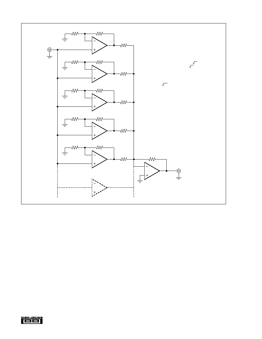
FIGURE 12. `N' Stage Parallel-Input Amplifier.
7
5
Output
Input
6
10k
1/2OPA2111
10k
100
1
3
2
10k
1/2OPA2111
10k
100
7
5
6
10k
1/2OPA2111
10k
100
1
3
2
10k
1/2OPA2111
10k
100
7
5
6
100
1
3
2
10k
1/2OPA2111
10k
100
6
3
2
OPA37
1/2OPA2111
10k
N = 10
5 each OPA2111BM
Since signal voltage sums directly with N
but amplifier noise voltage sums as N,
signal-to-noise ratio improves by N.
A
V
= ≠1010
e
n
= 1.9nV/ Hz typ
(1)
at 10kHz
BW = 30kHz typ
GBW = 30.3 MHz typ
V
OS
= ±16µV typ
(1)
V
OS
/
T = ±0.16µV/∞C typ
(1)
I
B
= 40pA max
Z
IN
= 10
12
|| 30pF
NOTE: (1) Theoretical performance
achievable from OPA2111BM
with uncorrelated random
distribution of parameters.
Æ
OPA2111
13
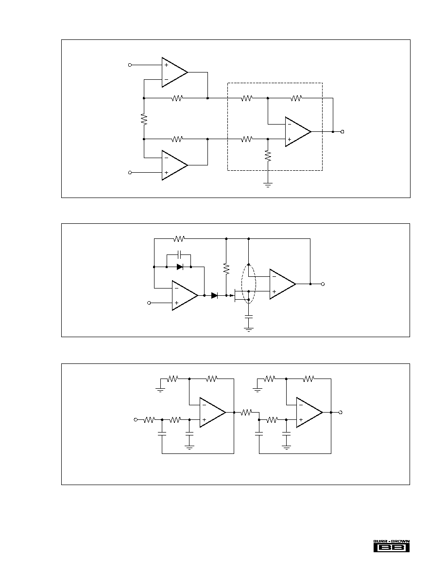
FIGURE 13. Precision Instrumentation Amplifier.
The information provided herein is believed to be reliable; however, BURR-BROWN assumes no responsibility for inaccuracies or omissions. BURR-BROWN assumes
no responsibility for the use of this information, and all use of such information shall be entirely at the user's own risk. Prices and specifications are subject to change
without notice. No patent rights or licenses to any of the circuits described herein are implied or granted to any third party. BURR-BROWN does not authorize or warrant
any BURR-BROWN product for use in life support devices and/or systems.
E
2
+In
R
1
202
1
E
1
≠In
R
2
10k
R
2
10k
2
3
E
O
Output
10k
100k
10k
100k
A
V
= 10
1
6
5
A
2
1/2 OPA2111
1/2 OPA2111
A
1
E
O
= 10(1 + 2 R
2
/R
1
)(E
2
≠ E
1
) = 1000(E
2
≠ E
1
)
INA106
Using the INA106 for an output difference amplifier extends the input common-mode
range of an instrumentation amplifier to
±
10V. A conventional IA with a unity-gain difference
amplifier has an input common-mode range limited to
±
5V for an output swing of
±
10V. This
is because a unity-gain difference amp needs
±
5V at the input for 10V at the output,
allowing only 5V additional for common-mode.