 | –≠–ª–µ–∫—Ç—Ä–æ–Ω–Ω—ã–π –∫–æ–º–ø–æ–Ω–µ–Ω—Ç: OPA2131 | –°–∫–∞—á–∞—Ç—å:  PDF PDF  ZIP ZIP |

OPA131
OPA2131
OPA4131
FEATURES
q
FET INPUT: I
B
= 50pA max
q
LOW OFFSET VOLTAGE: 750
µ
V max
q
WIDE SUPPLY RANGE:
±
4.5V to
±
18V
q
SLEW RATE: 10V/
µ
s
q
WIDE BANDWIDTH: 4MHz
q
EXCELLENT CAPACITIVE LOAD DRIVE
q
SINGLE, DUAL, QUAD VERSIONS
General Purpose
FET-INPUT OPERATIONAL AMPLIFIERS
DESCRIPTION
The OPA131 series of FET-input op amps provides
high performance at low cost. Single, dual and quad
versions in industry-standard pinouts allow cost-effec-
tive design options.
The OPA131 series offers excellent general purpose
performance, including low offset voltage, drift, and
good dynamic characteristics.
Single, dual and quad versions are available in DIP
and SOIC packages. Performance grades include com-
mercial and industrial temperature ranges.
1
2
3
4
5
6
7
14
13
12
11
10
9
8
Out D
≠In D
+In D
V≠
+In C
≠In C
Out C
Out A
≠In A
+In A
V+
+In B
≠In B
Out B
OPA4131
14-Pin DIP
SO-14
A
D
B
C
1
2
3
4
8
7
6
5
NC
V+
Output
Offset Trim
Offset Trim
≠In
+In
V≠
OPA131
8-Pin DIP, SO-8
1
2
3
4
5
6
7
8
16
15
14
13
12
11
10
9
Out D
≠In D
+In D
V≠
+In C
≠In C
Out C
NC
Out A
≠In A
+In A
V+
+In B
≠In B
Out B
NC
OPA4131
SOL-16
A
D
B
C
OPA131
OPA2
131
OPA131
OPA2131
OPA4131
OP
A4131
OPA4
131
International Airport Industrial Park ∑ Mailing Address: PO Box 11400 ∑ Tucson, AZ 85734 ∑ Street Address: 6730 S. Tucson Blvd. ∑ Tucson, AZ 85706
Tel: (520) 746-1111 ∑ Twx: 910-952-1111 ∑ Cable: BBRCORP ∑ Telex: 066-6491 ∑ FAX: (520) 889-1510 ∑ Immediate Product Info: (800) 548-6132
Æ
1
2
3
4
8
7
6
5
V+
Out B
≠In B
+In B
Out A
≠In A
+In A
V≠
OPA2131
8-Pin DIP, SO-8
A
B
© 1994 Burr-Brown Corporation
PDS-1256C
Printed in U.S.A. January, 1996

2
Æ
OPA131/2131/4131
SPECIFICATIONS
At T
A
= +25
∞
C, V
S
=
±
15V, and R
L
= 2k
,
unless otherwise noted.
The information provided herein is believed to be reliable; however, BURR-BROWN assumes no responsibility for inaccuracies or omissions. BURR-BROWN assumes
no responsibility for the use of this information, and all use of such information shall be entirely at the user's own risk. Prices and specifications are subject to change
without notice. No patent rights or licenses to any of the circuits described herein are implied or granted to any third party. BURR-BROWN does not authorize or warrant
any BURR-BROWN product for use in life support devices and/or systems.
OPA131PA, UA
OPA2131PA, UA
OPA4131PA, UA, NA
OPA131PJ, UJ
OPA2131PJ, UJ
OPA4131PJ, NJ
PARAMETER
CONDITION
MIN
TYP
MAX
MIN
TYP
MAX
UNITS
OFFSET VOLTAGE
Input Offset Voltage
±
0.2
±
1
*
±
1.5
mV
OPA131P, U models only
±
0.2
0.75
mV
vs Temperature
(1)
Operating Temperature Range
±
2
±
10
*
*
µ
V/
∞
C
vs Power Supply
V
S
=
±
4.5V to
±
18V
50
200
*
*
µ
V/V
OPA131P, U models only
50
100
µ
V/V
INPUT BIAS CURRENT
(2)
Input Bias Current
V
CM
= 0V
+5
±
50
*
*
pA
vs Temperature
See Typical Curve
*
Input Offset Current
V
CM
= 0V
±
1
±
50
*
*
pA
NOISE
Input Voltage Noise
Noise Density, f = 10Hz
21
*
nV/
Hz
f = 100Hz
16
*
nV/
Hz
f = 1kHz
15
*
nV/
Hz
f = 10kHz
15
*
nV/
Hz
Current Noise Density, f = 1kHz
3
*
fA/
Hz
INPUT VOLTAGE RANGE
Common-Mode Voltage Range
(V≠)+3
(V+)≠1
*
*
V
Common-Mode Rejection
V
CM
= ≠12V to +14V
70
80
*
*
dB
OPA131P, U models only
80
86
dB
INPUT IMPEDANCE
Differential
10
10
|| 1
*
|| pF
Common-Mode
V
CM
= 0V
10
12
|| 3
*
|| pF
OPEN-LOOP GAIN
Open-Loop Voltage Gain
V
O
= ≠12V to +12V
94
110
*
*
dB
OPA131P, U models only
100
110
dB
FREQUENCY RESPONSE
Gain-Bandwidth Product
4
*
MHz
Slew Rate
10
*
V/
µ
s
Settling Time 0.1%
G = ≠1, 10V Step, C
L
= 100pF
1.5
*
µ
s
0.01%
G = ≠1, 10V Step, C
L
= 100pF
2
*
µ
s
Total Harmonic Distortion + Noise
1kHz, G = 1, V
O
= 3.5Vrms
0.0008
*
%
OUTPUT
Voltage Output, Positive
(V+)≠3
(V+)≠2.5
*
*
V
Negative
(V≠)+3
(V≠)+2.5
*
*
V
Short-Circuit Current
±
25
*
mA
POWER SUPPLY
Specified Operating Voltage
±
15
*
V
Operating Voltage Range
±
4.5
±
18
*
*
V
Quiescent Current (per amplifier)
I
O
= 0
±
1.5
±
1.75
*
±
2
mA
TEMPERATURE RANGE
Operating Range
≠40
+85
0
+70
∞
C
Storage
≠40
+125
*
*
∞
C
Thermal Resistance,
JA
8-Pin DIP
100
*
∞
C/W
SO-8 Surface-Mount
150
*
∞
C/W
14-Pin DIP
80
*
∞
C/W
SO-14, SOL-16 Surface-Mount
110
*
∞
C/W
* Specifications same as OPA131PA, OPA131UA.
NOTES: (1) Guaranteed by wafer test. (2) High-speed test at T
J
= 25
∞
C.

3
OPA131/2131/4131
Æ
MODEL
PACKAGE
TEMPERATURE RANGE
Single
OPA131PJ
8-Pin Plastic DIP
0 to +70
∞
C
OPA131PA
8-Pin Plastic DIP
≠40
∞
C to +85
∞
C
OPA131P
8-Pin Plastic DIP
≠40
∞
C to +85
∞
C
OPA131UJ
SO-8 Surface-Mount
0 to +70
∞
C
OPA131UA
SO-8 Surface-Mount
≠40
∞
C to +85
∞
C
OPA131U
SO-8 Surface-Mount
≠40
∞
C to +85
∞
C
Dual
OPA2131PJ
8-Pin Plastic DIP
0 to +70
∞
C
OPA2131PA
8-Pin Plastic DIP
≠40
∞
C to +85
∞
C
OPA2131UJ
SO-8 Surface-Mount
0 to +70
∞
C
OPA2131UA
SO-8 Surface-Mount
≠40
∞
C to +85
∞
C
Quad
OPA4131PJ
14-Pin Plastic DIP
0 to +70
∞
C
OPA4131PA
14-Pin Plastic DIP
≠40
∞
C to +85
∞
C
OPA4131UA
SOL-16 Surface-Mount
≠40
∞
C to +85
∞
C
OPA4131NJ
SO-14 Surface-Mount
0 to +70
∞
C
OPA4131NA
SO-14 Surface-Mount
≠40
∞
C to +85
∞
C
PACKAGE INFORMATION
PACKAGE DRAWING
MODEL
PACKAGE
NUMBER
(1)
Single
OPA131PJ
8-Pin Plastic DIP
006
OPA131PA
8-Pin Plastic DIP
006
OPA131P
8-Pin Plastic DIP
006
OPA131UJ
SO-8 Surface-Mount
182
OPA131UA
SO-8 Surface-Mount
182
OPA131U
SO-8 Surface-Mount
182
Dual
OPA2131PJ
8-Pin Plastic DIP
006
OPA2131PA
8-Pin Plastic DIP
006
OPA2131UJ
SO-8 Surface-Mount
182
OPA2131UA
SO-8 Surface-Mount
182
Quad
OPA4131PJ
14-Pin Plastic DIP
010
OPA4131PA
14-Pin Plastic DIP
010
OPA4131UA
SOL-16 Surface-Mount
211
OPA4131NJ
SO-14 Surface-Mount
235
OPA4131NA
SO-14 Surface-Mount
235
NOTE: (1) For detailed drawing and dimension table, please see end of data
sheet, or Appendix D of Burr-Brown IC Data Book.
ELECTROSTATIC
DISCHARGE SENSITIVITY
This integrated circuit can be damaged by ESD. Burr-Brown
recommends that all integrated circuits be handled with
appropriate precautions. Failure to observe proper handling
and installation procedures can cause damage.
ESD damage can range from subtle performance degrada-
tion to complete device failure. Precision integrated circuits
may be more susceptible to damage because very small
parametric changes could cause the device not to meet its
published specifications.
ABSOLUTE MAXIMUM RATINGS
Supply Voltage, V+ to V≠ .................................................................... 36V
Input Voltage .................................................... (V≠) ≠0.7V to (V+) +0.7V
Output Short-Circuit
(1)
.............................................................. Continuous
Operating Temperature ................................................. ≠40
∞
C to +125
∞
C
Storage Temperature ..................................................... ≠40
∞
C to +125
∞
C
Junction Temperature ...................................................................... 150
∞
C
Lead Temperature (soldering, 10s) ................................................. 300
∞
C
NOTE: (1) Short-circuit to ground, one amplifier per package.
ORDERING INFORMATION

4
Æ
OPA131/2131/4131
TYPICAL PERFORMANCE CURVES
At T
A
= +25
∞
C, V
S
=
±
15V, and R
L
= 2k
,
unless otherwise noted.
POWER SUPPLY AND COMMON-MODE REJECTION
vs FREQUENCY
Frequency (Hz)
Power Supply Rejection (dB)
120
100
80
60
40
20
0
Common-Mode Rejection (dB)
120
100
80
60
40
20
0
10
100
1k
10k
100k
1M
CMR
+PSR
≠PSR
CHANNEL SEPARATION vs FREQUENCY
Frequency (Hz)
Channel Separation (dB)
160
140
120
100
80
10
100
1k
10k
100k
Dual and quad devices.
G = 1, all channels.
Quad measured channel
A to D or B to C--other
combinations yield improved
rejection.
R
L
=
R
L
= 2k
OPEN-LOOP GAIN/PHASE vs FREQUENCY
1
120
100
80
60
40
20
0
≠20
Voltage Gain (dB)
0
≠45
≠90
≠135
≠180
Phase Shift (∞)
Frequency (Hz)
10
100
1k
10k
100k
1M
10M
G
INPUT BIAS AND INPUT OFFSET CURRENT
vs TEMPERATURE
Ambient Temperature (∞C)
Input Bias and Input Offset Current (pA)
10k
1k
100
10
1
0.1
0.01
≠75
≠50
≠25
0
25
50
75
100
125
I
B
I
OS
V
CM
= 0V
INPUT BIAS CURRENT
vs INPUT COMMON-MODE VOLTAGE
Common-Mode Voltage (V)
Input Bias Current (pA)
1k
100
10
1
≠15
≠10
≠5
0
5
10
15
Input bias current is a
function of the voltage
between the V≠ supply
and the inputs.
V
S
= ±15V
V
S
= ±5V
INPUT VOLTAGE AND CURRENT NOISE
SPECTRAL DENSITY vs FREQUENCY
1
1k
100
10
Voltage Noise (nV/
Hz)
Frequency (Hz)
10
100
1k
10k
100k
1M
1
1k
100
10
Current Noise (fA/
Hz)
1
Voltage Noise
Current Noise
5
OPA131/2131/4131
Æ
TYPICAL PERFORMANCE CURVES
(CONT)
At T
A
= +25
∞
C, V
S
=
±
15V, and R
L
= 2k
,
unless otherwise noted.
QUIESCENT CURRENT AND SHORT-CIRCUIT CURRENT
vs TEMPERATURE
Temperature (∞C)
Quiescent Current (mA)
1.8
1.6
1.4
1.2
1
Short-Circuit Current (mA)
40
30
20
10
0
≠75
≠50
≠25
0
25
50
75
100
125
I
SC
+
I
SC
≠
I
Q
V
S
= ±5V
I
Q
V
S
= ±15V
OFFSET VOLTAGE DRIFT
PRODUCTION DISTRIBUTION
Units (%)
Offset Voltage Drift (µV/∞C)
≠7 ≠6 ≠5 ≠4 ≠3 ≠2 ≠1
0
1
2
3
4
5
6
7
35
30
25
20
15
10
5
0
Typical production distribution
of packaged units. Single,
dual and quad units included
OPEN-LOOP GAIN vs TEMPERATURE
Ambient Temperature (∞C)
Voltage Gain (dB)
120
115
110
105
100
≠75
≠50
≠25
0
25
50
75
100
125
OFFSET VOLTAGE
PRODUCTION DISTRIBUTION
Units (%)
Offset Voltage (µV)
≠1400
≠1200
≠1000
≠800
≠600
≠400
≠200
0
200
400
600
800
1000
1200
1400
20
15
10
5
0
Typical production distribution
of packaged units. Single,
dual and quad units included
TOTAL HARMONIC DISTORTION + NOISE
vs FREQUENCY
Frequency (Hz)
THD + Noise (%)
1
0.1
0.01
0.001
0.0001
10
100
1k
10k
100k
G = 1V/V
G = 100V/V
V
O
= 3.5Vrms
G = 10V/V
Bandwidth-
Limited
MAXIMUM OUTPUT VOLTAGE
vs FREQUENCY
1M
Frequency (Hz)
10k
100k
V
S
= ±5V
Maximum output voltage
without slew-rate induced
distortion
10M
30
20
10
0
Output Voltage (Vp-p)
V
S
= ±15V
6
Æ
OPA131/2131/4131
SMALL-SIGNAL STEP RESPONSE
G =1, C
L
= 300pF
200ns/div
50mV/div
TYPICAL PERFORMANCE CURVES
(CONT)
At T
CASE
= +25
∞
C, V
S
=
±
15V, and R
L
= 2k
, unless otherwise noted.
LARGE-SIGNAL STEP RESPONSE
G = 1, C
L
= 300pF
5V/div
1µs/div
SMALL-SIGNAL OVERSHOOT
vs LOAD CAPACITANCE
Load Capacitance
Overshoot (%)
50
40
30
20
10
0
100pF
1nF
10nF
R
L
= 2k
Higher R
L
value
generally reduces
overshoot.
G = +2
G = ≠1
G = ±10
G = 1
OUTPUT VOLTAGE SWING vs OUTPUT CURRENT
15
14
13
12
11
10
≠10
≠11
≠12
≠13
≠14
≠15
0
5
10
15
20
25
30
Output Current
(mA)
Output Voltage Swing (V)
≠55∞C
≠55∞C
25∞C
125∞C
125∞C
25∞C
V
IN
= ≠15V
V
IN
= 15V
SETTLING TIME vs CLOSED-LOOP GAIN
Closed-Loop Gain (V/V)
Settling Time (µs)
100
10
1
≠1
≠10
≠100
≠1000
V
O
= 10V Step
R
L
= 2k
C
L
= 100pF
0.1%
0.01%
7
OPA131/2131/4131
Æ
APPLICATIONS INFORMATION
OPA131 series op amps are unity-gain stable and suitable
for a wide range of general-purpose applications. Power
supply pins should be bypassed with 10nF ceramic capaci-
tors or larger.
OPA131 series op amps are free from unexpected output
phase-reversal common with FET op amps. Many FET-
input op amps exhibit phase-reversal of the output when the
input common-mode voltage range is exceeded. This can
occur in voltage-follower circuits, causing serious problems
in control loop applications. All circuitry is completely
independent in dual and quad versions, assuring normal
behavior when one amplifier in a package is overdriven or
short-circuited.
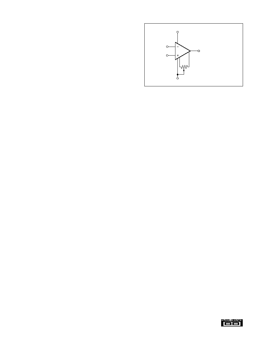
OFFSET VOLTAGE TRIM
The OPA131 (single op amp version) provides offset
voltage trim connections on pins 1 and 5. Offset voltage
can be adjusted by connecting a potentiometer as shown in
Figure 1. This adjustment should be used only to null the
offset of the op amp, not system offset or offset produced
by the signal source.
V+
V≠
100k
OPA131
(Single op amp only)
Trim Range: ±20mV typ
OPA131
6
7
5
4
3
2
1
FIGURE 1. OPA131 Offset Voltage Trim Circuit.
INPUT BIAS CURRENT
The input bias current is approximately 5pA at room tem-
perature and increases with temperature as shown in the
typical performance curve "Input Bias Current vs Tempera-
ture."
Input bias current also varies with common-mode voltage
and power supply voltage. This variation is dependent on the
voltage between the negative power supply and the com-
mon-mode input voltage. The effect is shown in the typical
curve "Input Bias Current vs Common-Mode Voltage."