Document Outline
- FEATURES
- DESCRIPTION
- APPLICATIONS
- ABSOLUTE MAXIMUM RATINGS
- PACKAGE/ORDERING INFORMATION
- PIN CONFIGURATIONS
- ELECTRICAL CHARACTERISTICS
- TYPICAL CHARACTERISTICS
- APPLICATIONS INFORMATION
- OPERATING VOLTAGE
- OPA334 ENABLE FUNCTION
- INPUT VOLTAGE
- INTERNAL OFFSET CORRECTIONS
- ACHIEVING OUTPUT SWING TO THE OP AMPS NEGATIVE RAIL
- LAYOUT GUIDELINES
- PACKAGE DRAWINGS
- DBV (R-PDSO-G6) PLASTIC SMALL-OUTLINE
- DGS (S-PDSO-G10)PLASTIC SMALL-OUTLINE PACKAGE
- DBV (R-PDSO-G5)PLASTIC SMALL-OUTLINE
- D (R-PDSO-G**)PLASTIC SMALL-OUTLINE PACKAGE
- DGK (R-PDSO-G8)PLASTIC SMALL-OUTLINE PACKAGE
PRODUCTION DATA information is current as of publication date.
Products conform to specifications per the terms of Texas Instruments
standard warranty. Production processing does not necessarily include
testing of all parameters.
APPLICATIONS
q
TRANSDUCER APPLICATIONS
q
TEMPERATURE MEASUREMENT
q
ELECTRONIC SCALES
q
MEDICAL INSTRUMENTATION
q
BATTERY-POWERED INSTRUMENTS
q
HANDHELD TEST EQUIPMENT
0.05
�
V/
�
C max, SINGLE-SUPPLY
CMOS OPERATIONAL AMPLIFIERS
Zer�-Drift Series
FEATURES
q
LOW OFFSET VOLTAGE: 5
�
V (max)
q
ZERO DRIFT: 0.05
�
V/
�
C (max)
q
QUIESCENT CURRENT: 285
�
A
q
SINGLE-SUPPLY OPERATION
q
SINGLE AND DUAL VERSIONS
q
SHUTDOWN
q
MicroSIZE
PACKAGES
DESCRIPTION
The OPA334 and OPA335 series of CMOS operational
amplifiers use auto-zeroing techniques to simultaneously
provide very low offset voltage (5
�
V max), and near-zero drift
over time and temperature. These miniature, high-precision,
low quiescent current amplifiers offer high input impedance
and rail-to-rail output swing. Single or dual supplies as low as
+2.7V (
�
1.35V) and up to +5.5V (
�
2.75V) may be used.
These op amps are optimized for low-voltage, single-supply
operation.
The OPA334 family includes a shutdown mode. Under logic
control, the amplifiers can be switched from normal operation
to a standby current of 2
�
A. When the Enable pin is con-
nected high, the amplifier is active. Connecting Enable low
disables the amplifier, and places the output in a high-
impedance state.
The OPA334 (single version with shutdown) comes in
MicroSIZE SOT23-6. The OPA335 (single version without
shutdown) is available in SOT23-5, and SO-8. The OPA2334
(dual version with shutdown) comes in
MicroSIZE MSOP-10.
The OPA2335 (dual version without shutdown) is offered in
the MSOP-8 and SO-8 packages. All versions are specified
for operation from �40
�
C to +125
�
C.
OPA334
OPA2334
OPA335
OPA2335
SBOS245D � JUNE 2002 � REVISED JULY 2003
Copyright � 2002-2003, Texas Instruments Incorporated
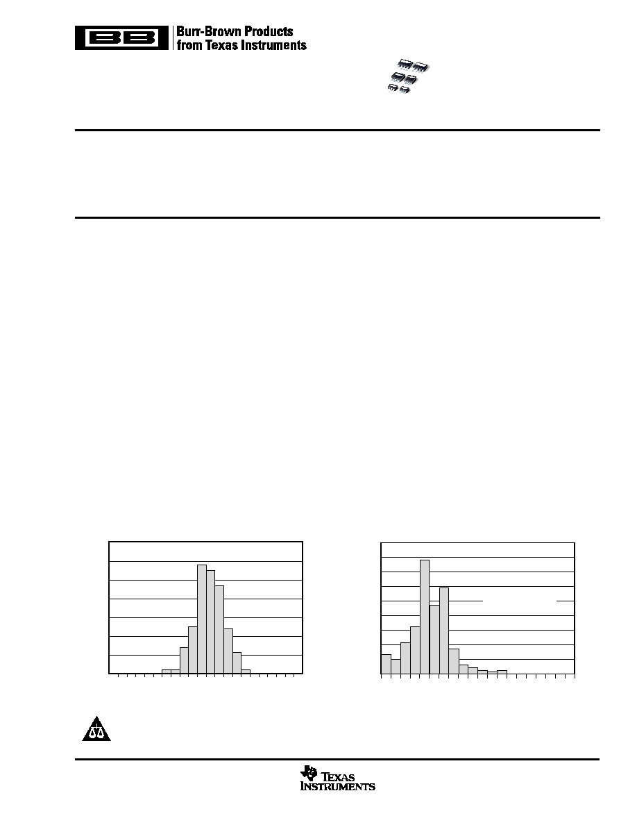
OFFSET VOLTAGE PRODUCTION DISTRIBUTION
Offset Voltage (
�
V)
�
3.0
�
2.7
�
2.4
�
2.1
�
1.8
�
1.5
�
1.2
�
0.9
�
0.6
�
0.3
0
0.3
0.6
0.9
1.2
1.5
1.8
2.1
2.4
2.7
3.0
Population
OFFSET VOLTAGE DRIFT PRODUCTION DISTRIBUTION
Offset Voltage Drift (
�
V/
�
C)
Population
0
0.005
0.010
0.015
0.020
0.025
0.030
0.035
0.040
0.045
0.050
Absolute Value;
Centered Around Zero
OPA2
334
OPA3
35
OPA2
335
OPA2
335
www.ti.com
Please be aware that an important notice concerning availability, standard warranty, and use in critical applications of
Texas Instruments semiconductor products and disclaimers thereto appears at the end of this data sheet.
All trademarks are the property of their respective owners.

2
www.ti.com
OPA334, OPA2334, OPA335, OPA2335
SBOS245D
SPECIFIED
PACKAGE
TEMPERATURE
PACKAGE
ORDERING
TRANSPORT
PRODUCT
PACKAGE-LEAD
DESIGNATOR
(1)
RANGE
MARKING
NUMBER
MEDIA, QUANTITY
Shutdown Version
OPA334
SOT23-6
DBV
�40
�
C to +125
�
C
OAOI
OPA334AIDBVT
Tape and Reel, 250
"
"
"
"
"
OPA334AIDBVR
Tape and Reel, 3000
OPA2334
MSOP-10
DGS
�40
�
C to +125
�
C
BHE
OPA2334AIDGST
Tape and Reel, 250
"
"
"
"
"
OPA2334AIDGSR
Tape and Reel, 2500
Non-Shutdown Version
OPA335
SOT23-5
DBV
�40
�
C to +125
�
C
OAPI
OPA335AIDBVT
Tape and Reel, 250
"
"
"
"
"
OPA335AIDBVR
Tape and Reel, 3000
OPA335
SO-8
D
�40
�
C to +125
�
C
OPA335
OPA335AID
Rails, 100
"
"
"
"
"
OPA335AIDR
Tape and Reel, 2500
OPA2335
SO-8
D
�40
�
C to +125
�
C
OPA2335
OPA2335AID
Rails, 100
"
"
"
"
"
OPA2335AIDR
Tape and Reel, 2500
OPA2335
MSOP-8
DGK
�40
�
C to +125
�
C
BHF
OPA2335AIDGKT
Tape and Reel, 250
"
"
"
"
"
OPA2335AIDGKR
Tape and Reel, 2500
NOTE: (1) For the most current specifications and package information, refer to our web site at www.ti.com.
Supply Voltage .................................................................................... +7V
Signal Input Terminals, Voltage
(2)
........................... �0.5V to (V+) + 0.5V
Current
(2)
..................................................
�
10mA
Output Short Circuit
(3)
.............................................................. Continuous
Operating Temperature .................................................. �40
�
C to +150
�
C
Storage Temperature ..................................................... �65
�
C to +150
�
C
Junction Temperature .................................................................... +150
�
C
Lead Temperature (soldering, 10s) ............................................... +300
�
C
NOTES: (1) Stresses above these ratings may cause permanent damage.
Exposure to absolute maximum conditions for extended periods may de-
grade device reliability. These are stress ratings only, and functional opera-
tion of the device at these, or any other conditions beyond those specified,
is not implied. (2) Input terminals are diode-clamped to the power-supply
rails. Input signals that can swing more than 0.5V beyond the supply rails
should be current-limited to 10mA or less. (3) Short-circuit to ground, one
amplifier per package.
ABSOLUTE MAXIMUM RATINGS
(1)
PACKAGE/ORDERING INFORMATION
ELECTROSTATIC
DISCHARGE SENSITIVITY
This integrated circuit can be damaged by ESD. Texas
Instruments recommends that all integrated circuits be handled
with appropriate precautions. Failure to observe proper han-
dling and installation procedures can cause damage.
ESD damage can range from subtle performance degrada-
tion to complete device failure. Precision integrated circuits
may be more susceptible to damage because very small
parametric changes could cause the device not to meet its
published specifications.
PIN CONFIGURATIONS
NOTES: (1) NC indicates no internal connection. (2) Pin 1 of the SOT23-6 is
determined by orienting the package marking as indicated in the diagram.
1
2
3
5
4
V+
�In
Out
V�
+In
OPA335
SOT23-5
1
2
3
4
8
7
6
5
NC
(1)
V+
Out
NC
(1)
NC
(1)
�In
+In
V�
OPA335
SO-8
1
2
3
4
8
7
6
5
V+
Out B
�In B
+In B
Out A
�In A
+In A
V�
OPA2335
SO-8, MSOP-8
A
B
1
2
3
6
5
4
V+
Enable
�In
Out
V�
+In
OPA334
(2)
OAOI
SOT23-6
1
2
3
4
5
10
9
8
7
6
V+
Out B
�In B
+In B
Enable B
Out A
�In A
+In A
V�
Enable A
OPA2334
MSOP-10
A
B
3
www.ti.com
OPA334, OPA2334, OPA335, OPA2335
SBOS245D
OPA334AI, OPA335AI
OPA2334AI, OPA2335AI
ELECTRICAL CHARACTERISTICS
Boldface limits apply over the specified temperature range, T
A
= �40
�
C to +125
�
C.
At T
A
= +25
�
C, V
S
= +5V,
R
L
= 10k
connected to V
S
/2, and V
OUT
= V
S
/2, unless otherwise noted.
PARAMETER
CONDITION
MIN
TYP
MAX
UNITS
OFFSET VOLTAGE
Input Offset Voltage
V
OS
V
CM
= V
S
/2
1
5
�
V
vs Temperature
dV
OS
/dT
�
0.02
�
0.05
�
V/
�
C
vs Power Supply
PSRR
V
S
= +2.7V to +5.5V, V
CM
= 0, Over Temperature
�
1
�
2
�
V/V
Long-Term Stability
(1)
See Note (1)
Channel Separation, dc
0.1
�
V/V
INPUT BIAS CURRENT
Input Bias Current
I
B
V
CM
= V
S
/2
�
70
�
200
pA
Over Temperature
1
nA
Input Offset Current
I
OS
�
120
�
400
pA
NOISE
Input Voltage Noise, f = 0.01Hz to 10Hz
e
n
1.4
�
V
PP
Input Current Noise Density, f = 10Hz
i
n
20
fA/
Hz
INPUT VOLTAGE RANGE
Common-Mode Voltage Range
V
CM
(V�) � 0.1
(V+) � 1.5
V
Common-Mode Rejection Ratio
CMRR
(V�) � 0.1V < V
CM
< (V+) � 1.5V, Over Temperature
110
130
dB
INPUT CAPACITANCE
Differential
1
pF
Common-Mode
5
pF
OPEN-LOOP GAIN
Open-Loop Voltage Gain, Over Temperature A
OL
50mV < V
O
< (V+) � 50mV, R
L
= 100k
, V
CM
= V
S
/2
110
130
dB
Over Temperature
100mV < V
O
< (V+) � 100mV, R
L
= 10k
, V
CM
= V
S
/2
110
130
dB
FREQUENCY RESPONSE
Gain-Bandwidth Product
GBW
2
MHz
Slew Rate
SR
G = +1
1.6
V/
�
s
OUTPUT
Voltage Output Swing from Rail
R
L
= 10k
, Over Temperature
15
100
mV
Voltage Output Swing from Rail
R
L
= 100k
, Over Temperature
1
50
mV
Short-Circuit Current
I
SC
�
50
mA
Capacitive Load Drive
C
LOAD
See Typical Characteristics
SHUTDOWN
t
OFF
1
�
s
t
ON
(2)
150
�
s
V
L
(shutdown)
0
+0.8
V
V
H
(amplifier is active)
0.75 (V+)
5.5
V
Input Bias Current of Enable Pin
50
pA
I
QSD
2
�
A
POWER SUPPLY
Operating Voltage Range
2.7
5.5
V
Quiescent Current: OPA334, OPA335
I
Q
I
O
= 0
285
350
�
A
Over Temperature
450
�
A
OPA2334, OPA2335 (total--two amplifiers)
I
O
= 0
570
700
�
A
Over Temperature
900
�
A
TEMPERATURE RANGE
Specified Range
�40
+125
�
C
Operating Range
�40
+150
�
C
Storage Range
�65
+150
�
C
Thermal Resistance
JA
�
C/W
SOT23-5, SOT23-6 Surface-Mount
200
�
C/W
MSOP-8, MSOP-10, SO-8 Surface-Mount
150
�
C/W
NOTES: (1) 500-hour life test at 150
�
C demonstrated randomly distributed variation approximately equal to measurement repeatability of 1
�
V. (2) Device requires
one complete cycle to return to V
OS
accuracy.
4
www.ti.com
OPA334, OPA2334, OPA335, OPA2335
SBOS245D
TYPICAL CHARACTERISTICS
At T
A
= +25
�
C, V
S
= +5V,
R
L
= 10k
connected to V
S
/2, and V
OUT
= V
S
/2, unless otherwise noted.
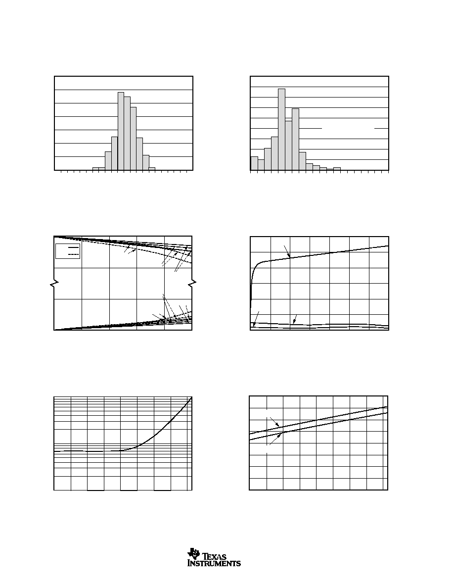
OFFSET VOLTAGE DRIFT PRODUCTION DISTRIBUTION
Offset Voltage Drift (
�
V/
�
C)
Population
0
0.005
0.010
0.015
0.020
0.025
0.030
0.035
0.040
0.045
0.050
Absolute Value;
Centered Around Zero
OFFSET VOLTAGE PRODUCTION DISTRIBUTION
Offset Voltage (
�
V)
�
3.0
�
2.7
�
2.4
�
2.1
�
1.8
�
1.5
�
1.2
�
0.9
�
0.6
�
0.3
0
0.3
0.6
0.9
1.2
1.5
1.8
2.1
2.4
2.7
3.0
Population
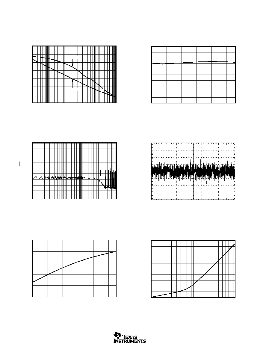
INPUT BIAS CURRENT vs COMMON-MODE VOLTAGE
Input Bias Current
(pA)
0
1200
1000
800
600
400
200
0
2.5
3.0
2.0
1.5
1.0
0.5
Common-Mode Voltage (V)
3.5
�40
�
C
+25
�
C
+125
�
C
INPUT BIAS CURRENT vs TEMPERATURE
Input Bias Current
(pA)
1000
100
10
Temperature (
�
C)
�40
40
20
0
�20
120
100
80
60
QUIESCENT CURRENT (per channel)
vs TEMPERATURE
Quiescent Current (
�
A)
�40
400
350
300
250
200
150
100
50
0
40
20
0
�20
Temperature (
�
C)
120
100
80
60
V
S
= +5.5V
V
S
= +2.7V
OUTPUT VOLTAGE SWING vs OUTPUT CURRENT
(V+)
(V+) � 1
(V�) + 1
(V�)
0
2
4
6
8
10
Output Current (mA)
Output Voltage Swing (V)
+125
�
C
5.5V
2.7V
+25
�
C
�40
�
C
+125
�
C
+25
�
C
�40
�
C
5
www.ti.com
OPA334, OPA2334, OPA335, OPA2335
SBOS245D
TYPICAL CHARACTERISTICS
(Cont.)
At T
A
= +25
�
C, V
S
= +5V,
R
L
= 10k
connected to V
S
/2, and V
OUT
= V
S
/2, unless otherwise noted.
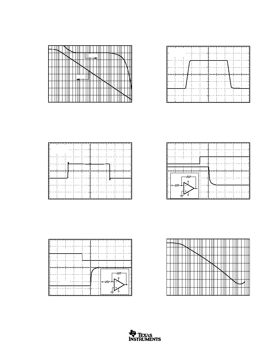
LARGE-SIGNAL RESPONSE
Time (5
�
s/div)
Output Voltage (1V/div)
G = �1
C
L
= 300pF
SMALL-SIGNAL RESPONSE
Time (5
�
s/div)
Output Voltage (50mV/div)
G = +1
C
L
= 50pF
OPEN-LOOP GAIN/PHASE vs FREQUENCY
A
OL
(dB)
140
120
100
80
60
40
20
0
�20
Phase (
�
)
�80
�90
�100
�110
�120
�130
�140
�150
�160
Frequency (Hz)
0.1
10k
1k
100
10
1
10M
1M
100k
Phase
Gain
POSITIVE OVER-VOLTAGE RECOVERY
Time (25
�
s/div)
200mV/div
1V/div
0
0
Input
Output
100
10k
+2.5V
�2.5V
OPA335
NEGATIVE OVER-VOLTAGE RECOVERY
Time (25
�
s/div)
200mV/div
1V/div
0
0
Input
Output
100
10k
+2.5V
�2.5V
OPA335
COMMON-MODE REJECTION vs FREQUENCY
Common-Mode Rejection (dB)
1
140
120
100
80
60
40
20
0
10k
1k
100
10
Frequency (Hz)
10M
1M
100k
6
www.ti.com
OPA334, OPA2334, OPA335, OPA2335
SBOS245D
TYPICAL CHARACTERISTICS
(Cont.)
At T
A
= +25
�
C, V
S
= +5V,
R
L
= 10k
connected to V
S
/2, and V
OUT
= V
S
/2, unless otherwise noted.
NOISE vs FREQUENCY
Noise (nV/
Hz)
1
1000
100
10
1k
100
10
Frequency (Hz)
100k
10k
SAMPLING FREQUENCY vs TEMPERATURE
Sampling Frequency (kHz)
�40
13
12
11
10
9
8
�10
50
110 125
Temperature (
�
C)
20
80
SAMPLING FREQUENCY vs SUPPLY VOLTAGE
Frequency (kHz)
2.7
11.0
10.9
10.8
10.7
10.6
10.5
10.4
10.3
10.2
10.1
10.0
3.7
3.2
5.2
5.5
Supply Voltage (V)
4.7
4.2
SMALL-SIGNAL OVERSHOOT vs LOAD CAPACITANCE
(V
S
= 2.7V to 5V)
Overshoot (%)
10
50
45
40
35
30
25
20
15
10
5
0
100
1000
Load Capacitance (pF)
R
L
= 10k
0.01Hz TO 10Hz NOISE
10s/div
400nV/div
POWER-SUPPLY REJECTION RATIO vs FREQUENCY
Power-Supply Rejection Ratio (dB)
140
120
100
80
60
40
20
0
Frequency (Hz)
10
1k
100
1M
100k
10k
+PSRR
�PSRR
7
www.ti.com
OPA334, OPA2334, OPA335, OPA2335
SBOS245D
TYPICAL CHARACTERISTICS
(Cont.)
At T
A
= +25
�
C, V
S
= +5V,
R
L
= 10k
connected to V
S
/2, and V
OUT
= V
S
/2, unless otherwise noted.
APPLICATIONS INFORMATION
The OPA334 and OPA335 series op amps are unity-gain
stable and free from unexpected output phase reversal. They
use auto-zeroing techniques to provide low offset voltage
and very low drift over time and temperature.
Good layout practice mandates use of a 0.1
�
F capacitor
placed closely across the supply pins.
For lowest offset voltage and precision performance, circuit
layout and mechanical conditions should be optimized. Avoid
temperature gradients that create thermoelectric (Seebeck)
effects in thermocouple junctions formed from connecting
dissimilar conductors. These thermally-generated potentials
can be made to cancel by assuring that they are equal on
both input terminals.
� Use low thermoelectric-coefficient connections (avoid dis-
similar metals).
� Thermally isolate components from power supplies or
other heat-sources.
� Shield op amp and input circuitry from air currents, such as
cooling fans.
Following these guidelines will reduce the likelihood of junc-
tions being at different temperatures, which can cause ther-
moelectric voltages of 0.1
�
V/
�
C or higher, depending on
materials used.
OPERATING VOLTAGE
The OPA334 and OPA335 series op amps operate over a
power-supply range of +2.7V to +5.5V (
�
1.35V to
�
2.75V).
Supply voltages higher than 7V (absolute maximum) can
permanently damage the amplifier. Parameters that vary
over supply voltage or temperature are shown in the Typical
Characteristics section of this data sheet.
OPA334 ENABLE FUNCTION
The enable/shutdown digital input is referenced to the V�
supply voltage of the amp. A logic high enables the op amp. A
valid logic high is defined as > 75% of the total supply voltage.
The valid logic high signal can be up to 5.5V above the negative
supply, independent of the positive supply voltage. A valid
logic low is defined as < 0.8V above the V� supply pin. If dual
or split power supplies are used, be sure that logic input signals
are properly referred to the negative supply voltage. The
Enable pin must be connected to a valid high or low voltage, or
driven, not left open circuit.
The logic input is a high-impedance CMOS input, with sepa-
rate logic inputs provided on the dual version. For battery-
operated applications, this feature can be used to greatly
reduce the average current and extend battery life.
The enable time is 150
�
s, which includes one full auto-zero
cycle required by the amplifier to return to V
OS
accuracy.
Prior to this time, the amplifier functions properly, but with
unspecified offset voltage.
Disable time is 1
�
s. When disabled, the output assumes a
high-impedance state. This allows the OPA334 to be oper-
ated as a gated amplifier, or to have the output multiplexed
onto a common analog output bus.
INPUT VOLTAGE
The input common-mode range extends from (V�) � 0.1V to
(V+) � 1.5V. For normal operation, the inputs must be limited
to this range. The common-mode rejection ratio is only valid
within the valid input common-mode range. A lower supply
voltage results in lower input common-mode range; there-
fore, attention to these values must be given when selecting
the input bias voltage. For example, when operating on a
single 3V power supply, common-mode range is from 0.1V
below ground to half the power-supply voltage.
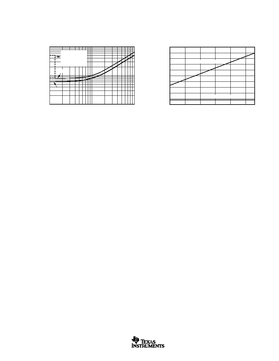
COMMON-MODE RANGE vs SUPPLY VOLTAGE
Common-Mode Range (V)
2.7
4.5
4.0
3.5
3.0
2.5
2.0
1.5
1.0
0.5
0
�0.5
3.7
3.2
5.2
5.5
Supply Voltage (V)
4.7
4.2
Minimum Common-Mode
Maximum Common-Mode
SETTLING TIME vs CLOSED-LOOP GAIN
Settling Time (
�
s)
1
100
10
1
10
Gain (V/V)
100
0.1%
0.01%
Unity-gain
requires one
complete Auto-Zero
Cycle--see text.
8
www.ti.com
OPA334, OPA2334, OPA335, OPA2335
SBOS245D
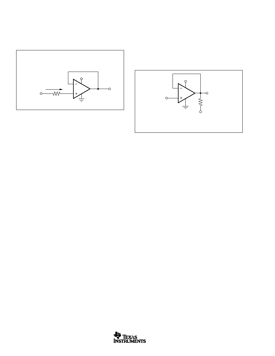
FIGURE 1. Input Current Protection.
5k
OPA335
10mA max
+5V
V
IN
V
OUT
I
OVERLOAD
Current-limiting resistor
required if input voltage
exceeds supply rails by
0.5V.
Normally, input bias current is approximately 70pA; however,
input voltages exceeding the power supplies can cause
excessive current to flow in or out of the input pins. Momen-
tary voltages greater than the power supply can be tolerated
if the input current is limited to 10mA. This is easily accom-
plished with an input resistor, as shown in Figure 1.
INTERNAL OFFSET CORRECTION
The OPA334 and OPA335 series op amps use an auto-zero
topology with a time-continuous 2MHz op amp in the signal
path. This amplifier is zero-corrected every 100
�
s using a
proprietary technique. Upon power-up, the amplifier requires
one full auto-zero cycle of approximately 100
�
s to achieve
specified V
OS
accuracy. Prior to this time, the amplifier
functions properly but with unspecified offset voltage.
This design has remarkably little aliasing and noise. Zero
correction occurs at a 10kHz rate, but there is virtually no
fundamental noise energy present at that frequency. For all
practical purposes, any glitches have energy at 20MHz or
higher and are easily filtered, if required. Most applications
are not sensitive to such high-frequency noise, and no
filtering is required.
Unity-gain operation demands that the auto-zero circuitry
correct for common-mode rejection errors of the main ampli-
fier. Because these errors can be larger than 0.01% of a full-
scale input step change, one calibration cycle (100
�
s) can be
required to achieve full accuracy. This behavior is shown in
the typical characteristic section, see
Settling Time vs Closed-
Loop Gain.
ACHIEVING OUTPUT SWING TO THE OP AMP'S
NEGATIVE RAIL
Some applications require output voltage swing from 0V to a
positive full-scale voltage (such as +2.5V) with excellent
accuracy. With most single-supply op amps, problems arise
when the output signal approaches 0V, near the lower output
FIGURE 2. Op Amp with Pull-Down Resistor to Achieve
V
OUT
= Ground.
swing limit of a single-supply op amp. A good single-supply
op amp may swing close to single-supply ground, but will not
reach ground. The output of the OPA334 or OPA335 can be
made to swing to ground, or slightly below, on a single-
supply power source. To do so requires use of another
resistor and an additional, more negative, power supply than
the op amp's negative supply. A pull-down resistor may be
connected between the output and the additional negative
supply to pull the output down below the value that the output
would otherwise achieve, as shown in Figure 2.
The OPA334 and OPA335 have an output stage that allows
the output voltage to be pulled to its negative supply rail, or
slightly below using the above technique. This technique only
works with some types of output stages. The OPA334 and
OPA335 have been characterized to perform well with this
technique. Accuracy is excellent down to 0V and as low as
�2mV. Limiting and non-linearity occurs below �2mV, but
excellent accuracy returns as the output is again driven
above �2mV. Lowering the resistance of the pull-down resis-
tor will allow the op amp to swing even further below the
negative rail. Resistances as low as 10k
can be used to
achieve excellent accuracy down to �10mV.
LAYOUT GUIDELINES
Attention to good layout practices is always recommended.
Keep traces short. When possible, use a PCB ground plane
with surface-mount components placed as close to the de-
vice pins as possible. Place a 0.1
�
F capacitor closely across
the supply pins. These guidelines should be applied through-
out the analog circuit to improve performance and provide
benefits such as reducing the EMI (electromagnetic-interfer-
ence) susceptibility.
V
OUT
R
P
= 40k
Op Amp's V�
= Gnd
OPA335
V
IN
V+ = +5V
�5V
Additional
Negative
Supply
9
www.ti.com
OPA334, OPA2334, OPA335, OPA2335
SBOS245D
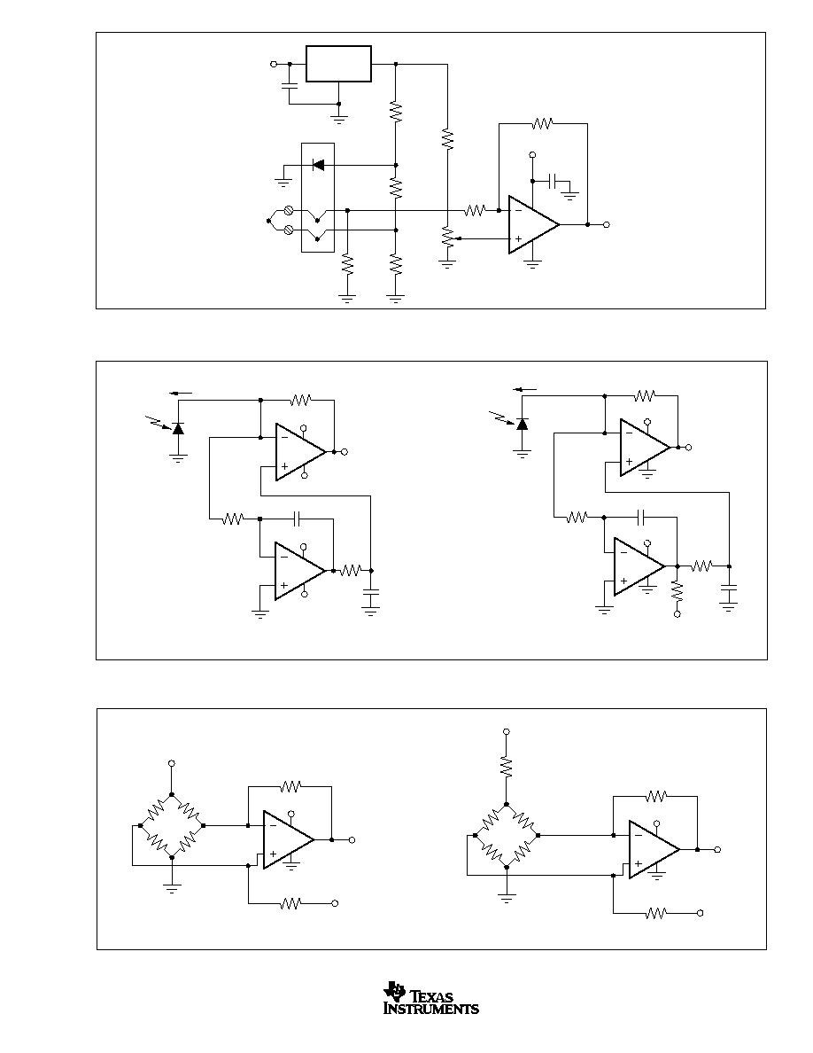
FIGURE 3. Temperature Measurement Circuit.
+
+
+
�
�
+
4.096V
0.1
�
F
+5V
Zero Adj.
K-Type
Thermocouple
40.7
�
V/
�
C
R
2
549
R
9
150k
R
5
31.6k
R
1
6.04k
R
6
200
+5V
0.1
�
F
R
2
2.94k
V
O
R
3
60.4
R
4
6.04k
OPA335
D1
REF3040
FIGURE 4. Auto-Zeroed Transimpedance Amplifier.
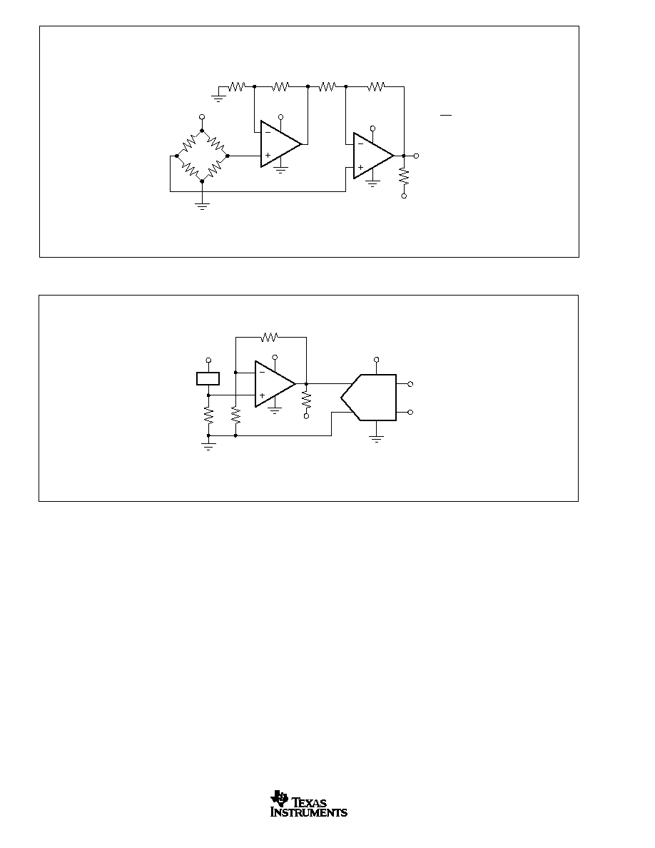
FIGURE 5. Single Op Amp Bridge Amplifier Circuits.
R
1
V
EX
V
OUT
V
REF
R
1
OPA335
R
R
R R
+5V
a. 5V Supply Bridge Amplifier.
V
EX
= +2.5V
R
1
= 105
@ V
S
= 2.7V,
V
CMmax
= 1.2V
V
OUT
OPA335
300
Bridge
+2.7V
R
2
Select R
1
so bridge
output
V
CMmax
.
V
REF
R
2
b. 2.7V Supply Bridge Amplifier.
1M
I
IN
R
1
R
2
C
1
C
2
40k
(1)
�5V
OPA343
OPA335
Photodiode
NOTE: (1) Optional pull-down
resistor to allow below
ground output swing.
+5V
+5V
b. Single Supply.
1M
I
IN
R
1
R
2
+2.5V
OPA343
�2.5V
+2.5V
C
1
C
2
�2.5V
OPA335
Photodiode
a. Split Supply.
10
www.ti.com
OPA334, OPA2334, OPA335, OPA2335
SBOS245D
FIGURE 7. Low-Side Current Measurement.
ADS1100
5V
V
11.5k
I
2
C
1k
R
S
Load
(PGA Gain = 8)
5V FS
50mV
Shunt
FS = 0.63V
G = 12.5
NOTE: (1) Pull-down resistor
to allow accurate swing to 0V.
�5V
R
3
(1)
40k
+5V
OPA335
FIGURE 6. Dual Op Amp IA Bridge Amplifier.
R
2
�5V
V
REF
R
3
(1)
40k
G = 1 +
R
2
R
1
R
1
R
1
+5V
+5V
R
2
1/2
OPA2335
R
R
R R
V
OUT
1/2
OPA2335
NOTE: (1) Optional pull-down resistor
to allow accurate swing to 0V.
11
www.ti.com
OPA334, OPA2334, OPA335, OPA2335
SBOS245D
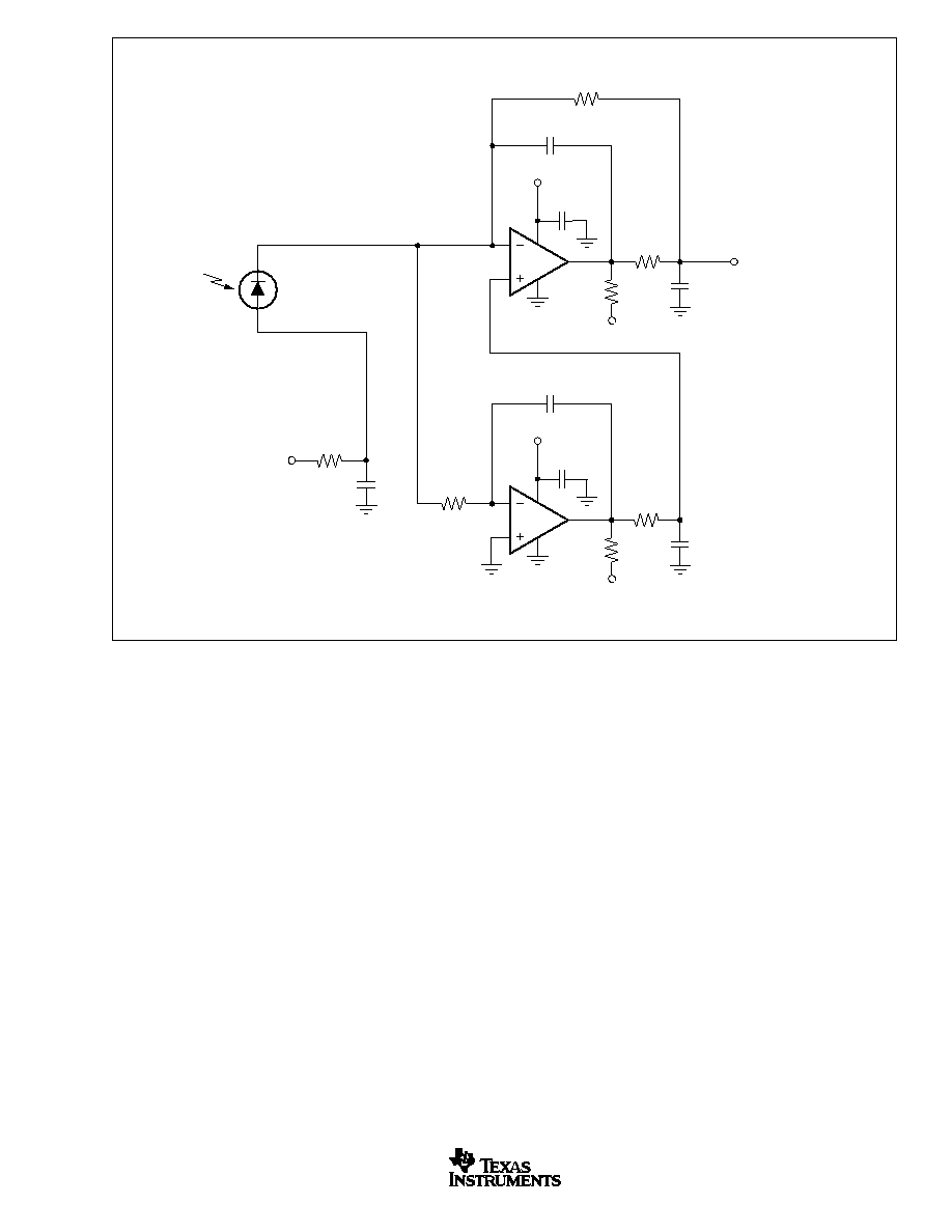
FIGURE 8. High Dynamic Range Transimpedance Amplifier.
�5V
R
2
(1)
2k
R
1
4.12k
+5V
R
3
100
V
OUT
1MHz Bandwidth
V
OS
10
�
V
OPA353
C
1
56pF
C
2
0.1
�
F
C
3
1nF
�5V
R
5
(1)
40k
+5V
R
6
49.9k
R
4
100k
OPA335
C
4
10nF
Photodiode
2pF
C
6
0.1
�
F
C
5
10nF
R
7
1k
Photodiode
Bias
C
7
1
�
F
NOTE: (1) Pull-down resistors to allow accurate swing to 0V.
12
www.ti.com
OPA334, OPA2334, OPA335, OPA2335
SBOS245D
PACKAGE DRAWINGS
DBV (R-PDSO-G6)
PLASTIC SMALL-OUTLINE
0,10
M
0,20
0,95
0 �8
0,25
0,55
0,35
Gage Plane
0,15 NOM
4073253-5/G 01/02
2,60
3,00
0,50
0,25
1,50
1,70
4
6
3
1
2,80
3,00
1,45
0,95
0,05 MIN
Seating Plane
6X
NOTES: A. All linear dimensions are in millimeters.
B. This drawing is subject to change without notice.
C. Body dimensions do not include mold flash or protrusion.
D. Leads 1, 2, 3 may be wider than leads 4, 5, 6 for package orientation.

13
www.ti.com
OPA334, OPA2334, OPA335, OPA2335
SBOS245D
DGS (S-PDSO-G10)
PLASTIC SMALL-OUTLINE PACKAGE
0,69
0,41
0,25
0,15 NOM
Gage Plane
4073272/B 08/01
4,98
0,17
6
3,05
4,78
2,95
10
5
3,05
2,95
1
0,27
0,15
0,05
1,07 MAX
Seating Plane
0,10
0,50
M
0,08
0
�
� 6
�
NOTES: A. All linear dimensions are in millimeters.
B. This drawing is subject to change without notice.
C. Body dimensions do not include mold flash or protrusion.
A. Falls within JEDEC MO-187
PACKAGE DRAWINGS (Cont.)
14
www.ti.com
OPA334, OPA2334, OPA335, OPA2335
SBOS245D
PACKAGE DRAWINGS (Cont.)
DBV (R-PDSO-G5)
PLASTIC SMALL-OUTLINE
0,10
M
0,20
0,95
0
�
� 8
�
0,25
0,35
0,55
Gage Plane
0,15 NOM
4073253-4/G 01/02
2,60
3,00
0,50
0,30
1,50
1,70
4
5
3
1
2,80
3,00
0,95
1,45
0,05 MIN
Seating Plane
NOTES: A. All linear dimensions are in millimeters.
B. This drawing is subject to change without notice.
C. Body dimensions do not include mold flash or protrusion.
D. Falls within JEDEC MO-178
15
www.ti.com
OPA334, OPA2334, OPA335, OPA2335
SBOS245D
PACKAGE DRAWINGS (Cont.)
D (R-PDSO-G**)
PLASTIC SMALL-OUTLINE PACKAGE
8 PINS SHOWN
8
0.197
(5,00)
A MAX
A MIN
(4,80)
0.189
0.337
(8,55)
(8,75)
0.344
14
0.386
(9,80)
(10,00)
0.394
16
DIM
PINS **
4040047/E 09/01
0.069 (1,75) MAX
Seating Plane
0.004 (0,10)
0.010 (0,25)
0.010 (0,25)
0.016 (0,40)
0.044 (1,12)
0.244 (6,20)
0.228 (5,80)
0.020 (0,51)
0.014 (0,35)
1
4
8
5
0.150 (3,81)
0.157 (4,00)
0.008 (0,20) NOM
0
�
� 8
�
Gage Plane
A
0.004 (0,10)
0.010 (0,25)
0.050 (1,27)
NOTES: A. All linear dimensions are in inches (millimeters).
B. This drawing is subject to change without notice.
C. Body dimensions do not include mold flash or protrusion, not to exceed 0.006 (0,15).
D. Falls within JEDEC MS-012
16
www.ti.com
OPA334, OPA2334, OPA335, OPA2335
SBOS245D
PACKAGE DRAWINGS (Cont.)
DGK (R-PDSO-G8)
PLASTIC SMALL-OUTLINE PACKAGE
0,69
0,41
0,25
0,15 NOM
Gage Plane
4073329/C 08/01
4,98
0,25
5
3,05
4,78
2,95
8
4
3,05
2,95
1
0,38
1,07 MAX
Seating Plane
0,65
M
0,08
0
�
� 6
�
0,10
0,15
0,05
NOTES: A. All linear dimensions are in millimeters.
B. This drawing is subject to change without notice.
C. Body dimensions do not include mold flash or protrusion.
D. Falls within JEDEC MO-187
PACKAGING INFORMATION
ORDERABLE DEVICE
STATUS(1)
PACKAGE TYPE
PACKAGE DRAWING
PINS
PACKAGE QTY
OPA2334AIDGSR
ACTIVE
VSSOP
DGS
10
2500
OPA2334AIDGST
ACTIVE
VSSOP
DGS
10
250
OPA2335AID
ACTIVE
SOIC
D
8
100
OPA2335AIDGKR
ACTIVE
VSSOP
DGK
8
2500
OPA2335AIDGKT
ACTIVE
VSSOP
DGK
8
250
OPA2335AIDR
ACTIVE
SOIC
D
8
2500
OPA334AIDBVR
ACTIVE
SOP
DBV
6
3000
OPA334AIDBVT
ACTIVE
SOP
DBV
6
250
OPA335AID
ACTIVE
SOIC
D
8
100
OPA335AIDBVR
ACTIVE
SOP
DBV
5
3000
OPA335AIDBVT
ACTIVE
SOP
DBV
5
250
OPA335AIDR
ACTIVE
SOIC
D
8
2500
(1) The marketing status values are defined as follows:
ACTIVE: Product device recommended for new designs.
LIFEBUY: TI has announced that the device will be discontinued, and a lifetime-buy period is in effect.
NRND: Not recommended for new designs. Device is in production to support existing customers, but TI does not recommend using this part in
a new design.
PREVIEW: Device has been announced but is not in production. Samples may or may not be available.
OBSOLETE: TI has discontinued the production of the device.
PACKAGE OPTION ADDENDUM
www.ti.com
8-Sep-2004

IMPORTANT NOTICE
Texas Instruments Incorporated and its subsidiaries (TI) reserve the right to make corrections, modifications,
enhancements, improvements, and other changes to its products and services at any time and to discontinue
any product or service without notice. Customers should obtain the latest relevant information before placing
orders and should verify that such information is current and complete. All products are sold subject to TI's terms
and conditions of sale supplied at the time of order acknowledgment.
TI warrants performance of its hardware products to the specifications applicable at the time of sale in
accordance with TI's standard warranty. Testing and other quality control techniques are used to the extent TI
deems necessary to support this warranty. Except where mandated by government requirements, testing of all
parameters of each product is not necessarily performed.
TI assumes no liability for applications assistance or customer product design. Customers are responsible for
their products and applications using TI components. To minimize the risks associated with customer products
and applications, customers should provide adequate design and operating safeguards.
TI does not warrant or represent that any license, either express or implied, is granted under any TI patent right,
copyright, mask work right, or other TI intellectual property right relating to any combination, machine, or process
in which TI products or services are used. Information published by TI regarding third-party products or services
does not constitute a license from TI to use such products or services or a warranty or endorsement thereof.
Use of such information may require a license from a third party under the patents or other intellectual property
of the third party, or a license from TI under the patents or other intellectual property of TI.
Reproduction of information in TI data books or data sheets is permissible only if reproduction is without
alteration and is accompanied by all associated warranties, conditions, limitations, and notices. Reproduction
of this information with alteration is an unfair and deceptive business practice. TI is not responsible or liable for
such altered documentation.
Resale of TI products or services with statements different from or beyond the parameters stated by TI for that
product or service voids all express and any implied warranties for the associated TI product or service and
is an unfair and deceptive business practice. TI is not responsible or liable for any such statements.
Following are URLs where you can obtain information on other Texas Instruments products and application
solutions:
Products
Applications
Amplifiers
amplifier.ti.com
Audio
www.ti.com/audio
Data Converters
dataconverter.ti.com
Automotive
www.ti.com/automotive
DSP
dsp.ti.com
Broadband
www.ti.com/broadband
Interface
interface.ti.com
Digital Control
www.ti.com/digitalcontrol
Logic
logic.ti.com
Military
www.ti.com/military
Power Mgmt
power.ti.com
Optical Networking
www.ti.com/opticalnetwork
Microcontrollers
microcontroller.ti.com
Security
www.ti.com/security
Telephony
www.ti.com/telephony
Video & Imaging
www.ti.com/video
Wireless
www.ti.com/wireless
Mailing Address:
Texas Instruments
Post Office Box 655303 Dallas, Texas 75265
Copyright
2004, Texas Instruments Incorporated