 | –≠–ª–µ–∫—Ç—Ä–æ–Ω–Ω—ã–π –∫–æ–º–ø–æ–Ω–µ–Ω—Ç: OPA2340EA | –°–∫–∞—á–∞—Ç—å:  PDF PDF  ZIP ZIP |
1
Æ
OPA340/2340/4340
1
2
3
4
5
6
7
8
16
15
14
13
12
11
10
9
Out D
≠In D
+In D
≠V
+In C
≠In C
Out C
NC
Out A
≠In A
+In A
+V
+In B
≠In B
Out B
NC
OPA4340
SSOP-16
A
D
B
C
1
2
3
4
8
7
6
5
V+
Out B
≠In B
+In B
Out A
≠In A
+In A
V≠
OPA2340
8-Pin DIP, SO-8, MSOP-8
A
B
1
2
3
4
8
7
6
5
NC
V+
Output
NC
NC
≠In
+In
V≠
OPA340
8-Pin DIP, SO-8
1
2
3
5
4
V+
≠In
Out
V≠
+In
OPA340
SOT-23-5
SINGLE-SUPPLY, RAIL-TO-RAIL
OPERATIONAL AMPLIFIERS
Micro
Amplifier
TM
Series
FEATURES
q
RAIL-TO-RAIL INPUT
q
RAIL-TO-RAIL OUTPUT (within 1mV)
q
Micro
SIZE PACKAGES
q
WIDE BANDWIDTH: 5.5MHz
q
HIGH SLEW RATE: 6V/
µ
s
q
LOW THD+NOISE: 0.0007% (f = 1kHz)
q
LOW QUIESCENT CURRENT: 750
µ
A/channel
q
SINGLE, DUAL, AND QUAD
International Airport Industrial Park ∑ Mailing Address: PO Box 11400, Tucson, AZ 85734 ∑ Street Address: 6730 S. Tucson Blvd., Tucson, AZ 85706 ∑ Tel: (520) 746-1111 ∑ Twx: 910-952-1111
Internet: http://www.burr-brown.com/ ∑ FAXLine: (800) 548-6133 (US/Canada Only) ∑ Cable: BBRCORP ∑ Telex: 066-6491 ∑ FAX: (520) 889-1510 ∑ Immediate Product Info: (800) 548-6132
APPLICATIONS
q
DRIVING A/D CONVERTERS
q
PCMCIA CARDS
q
DATA ACQUISITION
q
PROCESS CONTROL
q
AUDIO PROCESSING
q
COMMUNICATIONS
q
ACTIVE FILTERS
q
TEST EQUIPMENT
DESCRIPTION
OPA340 series rail-to-rail CMOS operational amplifi-
ers are optimized for low voltage, single supply opera-
tion. Rail-to-rail input/output and high speed operation
make them ideal for driving sampling analog-to-digital
converters. They are also well suited for general pur-
pose and audio applications as well as providing I/V
conversion at the output of D/A converters. Single,
dual, and quad versions have identical specifications
for design flexibility.
The OPA340 series operates on a single supply as low as
2.5V with an input common-mode voltage range that
extends 500mV below ground and 500mV above the
positive supply. Output voltage swing is to within 1mV
of the supply rails with a 100k
load. They offer excel-
lent dynamic response (BW = 5.5MHz, SR = 6V/
µ
s), yet
quiescent current is only 750
µ
A. Dual and quad designs
feature completely independent circuitry for lowest
crosstalk and freedom from interaction.
The single (OPA340) packages are the tiny 5-lead
SOT-23-5 surface mount, SO-8 surface mount, and
8-pin DIP. The dual (OPA2340) comes in the minia-
ture MSOP-8 surface mount, SO-8 surface mount,
and 8-pin DIP packages. The quad (OPA4340) pack-
ages are the space-saving SSOP-16 surface mount,
SO-14 surface mount, and the 14-pin DIP. All are
specified from ≠40
∞
C to +85
∞
C and operate from
≠55
∞
C to +125
∞
C. A SPICE macromodel is available
for design analysis.
OPA4340
OPA340
OPA2340
OPA4340
Æ
OPA340
OPA2340
OPA4340
© 1997 Burr-Brown Corporation
PDS-1404C
Printed in U.S.A. December, 1997
2
Æ
OPA340/2340/4340
SPECIFICATIONS: V
S
= 2.7V to 5V
At T
A
= +25
∞
C, R
L
= 10k
connected to V
S
/2 and V
OUT
= V
S
/2, unless otherwise noted.
Boldface limits apply over the specified temperature range, T
A
= ≠40
∞
C to +85
∞
C. V
S
= 5V.
PARAMETER
CONDITION
MIN
TYP
(1)
MAX
UNITS
OFFSET VOLTAGE
Input Offset Voltage
V
OS
V
S
= 5V
±
150
±
500
µ
V
vs Temperature
dV
OS
/dT
±
2.5
µ
V/
∞
C
vs Power Supply
PSRR
V
S
= 2.7V to 5.5V, V
CM
= 0V
30
120
µ
V/V
T
A
= ≠40
∞
C to +85
∞
C
V
S
= 2.7V to 5.5V, V
CM
= 0V
120
µ
V/V
Channel Separation, dc
0.2
µ
V/V
INPUT BIAS CURRENT
Input Bias Current
I
B
±
0.2
±
10
pA
T
A
= ≠40
∞
C to +85
∞
C
±
60
pA
Input Offset Current
I
OS
±
0.2
±
10
pA
NOISE
Input Voltage Noise, f = 0.1 to 50kHz
8
µ
Vrms
Input Voltage Noise Density, f = 1kHz
e
n
25
nV/
Hz
Current Noise Density, f = 1kHz
i
n
3
fA/
Hz
INPUT VOLTAGE RANGE
Common-Mode Voltage Range
V
CM
≠0.3
(V+) +0.3
V
Common-Mode Rejection Ratio
CMRR
≠0.3V < V
CM
< (V+) ≠1.8V
80
92
dB
V
S
= 5V, ≠0.3V
< V
CM
< 5.3V
70
84
dB
V
S
= 2.7V, ≠0.3V
< V
CM
< 3V
66
80
dB
INPUT IMPEDANCE
Differential
10
13
|| 3
|| pF
Common-Mode
10
13
|| 6
|| pF
OPEN-LOOP GAIN
Open-Loop Voltage Gain
A
OL
R
L
= 100k
, 5mV < V
O
< (V+) ≠5mV
106
124
dB
T
A
= ≠40
∞
C to +85
∞
C
R
L
= 100k
, 5mV < V
O
< (V+) ≠5mV
106
dB
R
L
= 10k
, 50mV < V
O
< (V+) ≠50mV
100
120
dB
T
A
= ≠40
∞
C to +85
∞
C
R
L
= 10k
, 50mV < V
O
< (V+) ≠50mV
100
dB
R
L
= 2k
, 200mV < V
O
< (V+) ≠200mV
94
114
dB
T
A
= ≠40
∞
C to +85
∞
C
R
L
= 2k
, 200mV < V
O
< (V+) ≠200mV
94
dB
FREQUENCY RESPONSE
Gain-Bandwidth Product
GBW
G = 1
5.5
MHz
Slew Rate
SR
V
S
= 5V, G = 1, C
L
= 100pF
6
V/
µ
s
Settling Time, 0.1%
V
S
= 5V, 2V Step, C
L
= 100pF
1
µ
s
0.01%
V
S
= 5V, 2V Step, C
L
= 100pF
1.6
µ
s
Overload Recovery Time
V
IN
∑ G = V
S
0.2
µ
s
Total Harmonic Distortion + Noise
THD+N
V
S
= 5V, V
O
= 3Vp-p
(2)
, G = 1, f = 1kHz
0.0007
%
OUTPUT
Voltage Output Swing from Rail
(3)
R
L
= 100k
, A
OL
106dB
1
5
mV
T
A
= ≠40
∞
C to +85
∞
C
R
L
= 100k
,
A
OL
106dB
5
mV
R
L
= 10k
,
A
OL
100dB
10
50
mV
T
A
= ≠40
∞
C to +85
∞
C
R
L
= 10k
, A
OL
100dB
50
mV
R
L
= 2k
,
A
OL
94dB
40
200
mV
T
A
= ≠40
∞
C to +85
∞
C
R
L
= 2k
, A
OL
94dB
200
mV
Short-Circuit Current
I
SC
±
50
mA
Capacitive Load Drive
C
LOAD
See Typical Curve
POWER SUPPLY
Specified Voltage Range
V
S
2.7
5
V
Operating Voltage Range
2.5 to 5.5
V
Quiescent Current (per amplifier)
I
Q
I
O
= 0, V
S
= +5V
750
950
µ
A
T
A
= ≠40
∞
C to +85
∞
C
I
O
= 0, V
S
= +5V
1100
µ
A
TEMPERATURE RANGE
Specified Range
≠40
+85
∞
C
Operating Range
≠55
+125
∞
C
Storage Range
≠55
+125
∞
C
Thermal Resistance
JA
SOT-23-5 Surface Mount
200
∞
C/W
MSOP-8 Surface Mount
150
∞
C/W
SO-8 Surface Mount
150
∞
C/W
8-Pin DIP
100
∞
C/W
SSOP-16 Surface Mount
100
∞
C/W
SO-14 Surface Mount
100
∞
C/W
14-Pin DIP
80
∞
C/W
NOTES: (1) V
S
= +5V. (2) V
OUT
= 0.25V to 3.25V. (3) Output voltage swings are measured between the output and power supply rails.
OPA340NA, PA, UA
OPA2340EA, PA, UA
OPA4340EA, PA, UA
3
Æ
OPA340/2340/4340
1
2
3
4
5
6
7
14
13
12
11
10
9
8
Out D
≠In D
+In D
V≠
+In C
≠In C
Out C
Out A
≠In A
+In A
V+
+In B
≠In B
Out B
OPA4340
A
D
B
C
PACKAGE/ORDERING INFORMATION
Supply Voltage ................................................................................... 5.5V
Signal Input Terminals, Voltage
(2)
.................... (V≠) ≠0.5V to (V+) +0.5V
Current
(2)
.................................................... 10mA
Output Short-Circuit
(3)
.............................................................. Continuous
Operating Temperature ................................................. ≠55
∞
C to +125
∞
C
Storage Temperature ..................................................... ≠55
∞
C to +125
∞
C
Junction Temperature ...................................................................... 150
∞
C
Lead Temperature (soldering, 10s) ................................................. 300
∞
C
NOTES: (1) Stresses above these ratings may cause permanent damage.
(2) Input terminals are diode-clamped to the power supply rails. Input signals
that can swing more than 0.5V beyond the supply rails should be current-
limited to 10mA or less. (3) Short-circuit to ground, one amplifier per
package.
ABSOLUTE MAXIMUM RATINGS
(1)
PIN CONFIGURATIONS
Top View
SOIC/DIP
PACKAGE
SPECIFIED
DRAWING
TEMPERATURE
PACKAGE
ORDERING
TRANSPORT
PRODUCT
PACKAGE
NUMBER
(1)
RANGE
MARKING
NUMBER
(2)
MEDIA
Single
OPA340NA
5-Lead SOT-23-5
331
≠40
∞
C to +85
∞
C
A40
OPA340NA-250
Tape and Reel
"
"
"
"
"
OPA340NA-3K
Tape and Reel
OPA340PA
8-Pin DIP
006
≠40
∞
C to +85
∞
C
OPA340PA
OPA340PA
Rails
OPA340UA
SO-8 Surface-Mount
182
≠40
∞
C to +85
∞
C
OPA340UA
OPA340UA
Rails
(3)
Dual
OPA2340EA
MSOP-8 Surface-Mount
337
≠40
∞
C to +85
∞
C
A40A
OPA2340EA-250
Tape and Reel
"
"
"
"
"
OPA2340EA-2500
Tape and Reel
OPA2340PA
8-Pin DIP
006
≠40
∞
C to +85
∞
C
OPA2340PA
OPA2340PA
Rails
OPA2340UA
SO-8 Surface-Mount
182
≠40
∞
C to +85
∞
C
OPA2340UA
OPA2340UA
Rails
(3)
Quad
OPA4340EA
SSOP-16 Surface-Mount
322
≠40
∞
C to +85
∞
C
OPA4340EA
OPA4340EA-250
Tape and Reel
"
"
"
"
"
OPA4340EA-2500
Tape and Reel
OPA4340PA
14-Pin DIP
010
≠40
∞
C to +85
∞
C
OPA4340PA
OPA4340PA
Rails
OPA4340UA
SO-14 Surface Mount
235
≠40
∞
C to +85
∞
C
OPA4340UA
OPA4340UA
Rails
(3)
NOTES: (1) For detailed drawing and dimension table, please see end of data sheet, or Appendix C of Burr-Brown IC Data Book. (2) Models with -250, -2500, and
-3K are available only in Tape and Reel in the quantities indicated (e.g., -250 indicates 250 devices per reel). Ordering 3000 pieces of "OPA340NA-3K" will get
a single 3000 piece Tape and Reel. For detailed Tape and Reel mechanical information, refer to Appendix B of Burr-Brown IC Data Book. (3) SO-8 and SO-14
models also available in Tape and Reel.
The information provided herein is believed to be reliable; however, BURR-BROWN assumes no responsibility for inaccuracies or omissions. BURR-BROWN assumes no responsibility
for the use of this information, and all use of such information shall be entirely at the user's own risk. Prices and specifications are subject to change without notice. No patent rights or
licenses to any of the circuits described herein are implied or granted to any third party. BURR-BROWN does not authorize or warrant any BURR-BROWN product for use in life support
devices and/or systems.
ELECTROSTATIC
DISCHARGE SENSITIVITY
This integrated circuit can be damaged by ESD. Burr-Brown
recommends that all integrated circuits be handled with
appropriate precautions. Failure to observe proper handling
and installation procedures can cause damage.
ESD damage can range from subtle performance degrada-
tion to complete device failure. Precision integrated circuits
may be more susceptible to damage because very small
parametric changes could cause the device not to meet its
published specifications.
4
Æ
OPA340/2340/4340
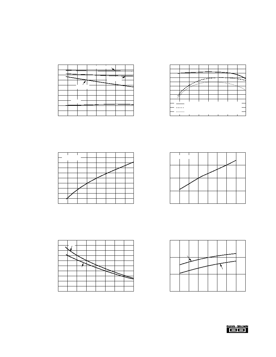
TYPICAL PERFORMANCE CURVES
At T
A
= +25
∞
C, V
S
= +5V, and R
L
= 10k
connected to V
S
/2, unless otherwise noted.
CLOSED-LOOP OUTPUT IMPEDANCE
vs FREQUENCY
5k
4k
3k
2k
1k
0
Output Resistance (
)
Frequency (Hz)
10
100
1k
10k
100k
1M
10M
G = 100
G = 10
G = 1
CHANNEL SEPARATION vs FREQUENCY
Frequency (Hz)
Channel Separation (dB)
140
130
120
110
100
100
10
1k
10k
100k
G = 1, All Channels
OPEN-LOOP GAIN/PHASE vs FREQUENCY
0.1
1
160
140
120
100
80
60
40
20
0
≠20
Voltage Gain (dB)
0
≠45
≠90
≠135
≠180
Phase (∞)
Frequency (Hz)
10
100
1k
10k
100k
1M
10M
INPUT VOLTAGE AND CURRENT NOISE
SPECTRAL DENSITY vs FREQUENCY
10k
1k
100
10
1
1k
100
10
1
0.1
Voltage Noise (nV
Hz)
Frequency (Hz)
1
10
100
1k
10k
100k
1M
Current Noise (fA
Hz)
Current Noise
Voltage Noise
TOTAL HARMONIC DISTORTION + NOISE
vs FREQUENCY
0.1
0.01
0.001
0.0001
THD+N (%)
Frequency (Hz)
20
100
1k
10k
20k
R
L
= 600
G = 10
G = 1
R
L
= 2k
R
L
= 2k
R
L
= 10k
R
L
= 600
R
L
= 10k
POWER SUPPLY and COMMON-MODE
REJECTION vs FREQUENCY
100
80
60
40
20
0
PSRR, CMRR (dB)
Frequency (Hz)
1
10
100
1k
10k
100k
1M
PSRR
CMRR
5
Æ
OPA340/2340/4340
TYPICAL PERFORMANCE CURVES
(CONT)
At T
A
= +25
∞
C, V
S
= +5V, and R
L
= 10k
connected to V
S
/2, unless otherwise noted.
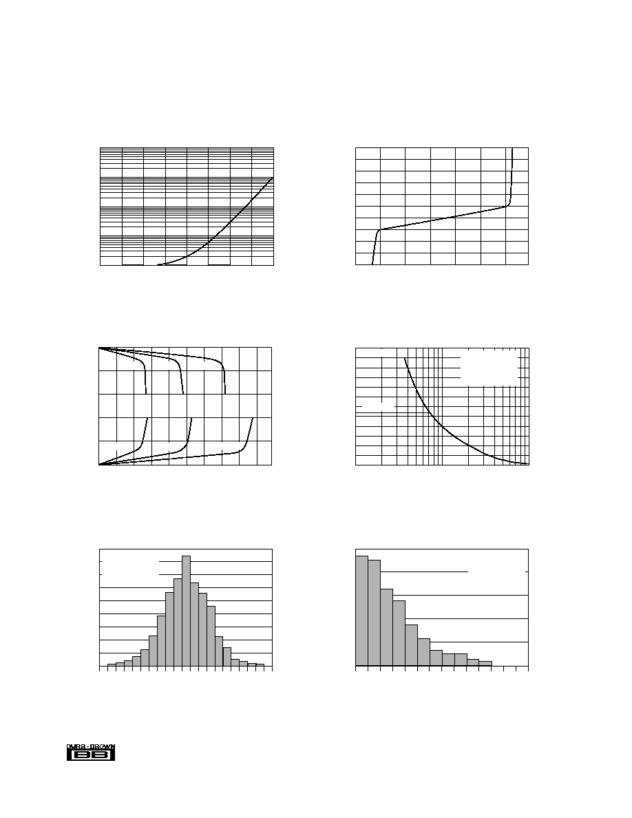
QUIESCENT CURRENT vs TEMPERATURE
1000
900
800
700
600
500
Quiescent Current (µA)
Temperature (∞C)
≠75
≠50
≠25
0
25
50
75
100
125
Per Amplifier
SHORT-CIRCUIT CURRENT vs TEMPERATURE
Temperature (∞C)
Short-Circuit Current (mA)
100
90
80
70
60
50
40
30
20
10
0
≠75
≠50
≠25
0
25
50
75
100
125
≠I
SC
+I
SC
SHORT-CIRCUIT CURRENT vs SUPPLY VOLTAGE
Supply Voltage (V)
Short-Circuit Current (mA)
60
50
40
30
2.0
2.5
3.0
3.5
4.0
4.5
5.0
5.5
6.0
+I
SC
≠I
SC
COMMON-MODE REJECTION vs TEMPERATURE
100
90
80
70
60
50
40
CMRR (dB)
Temperature (∞C)
≠75
≠50
≠25
0
25
50
75
100
125
V
S
= 5V, V
CM
= ≠0.3V to 5.3V
V
S
= 2.7V, V
CM
= ≠0.3V to 3V
V
S
= 2.7V to 5V, V
CM
= ≠0.3V to (V+) ≠1.8V
QUIESCENT CURRENT vs SUPPLY VOLTAGE
Supply Voltage (V)
Quiescent Current (
µ
A)
800
750
700
650
600
2.0
2.5
3.0
3.5
4.0
4.5
5.0
5.5
6.0
Per Amplifier
OPEN-LOOP GAIN AND POWER SUPPLY REJECTION
vs TEMPERATURE
130
120
110
100
90
80
A
OL
, PSRR (dB)
Temperature (∞C)
≠75
≠50
≠25
0
25
50
75
100
125
R
L
= 100k
R
L
= 10k
R
L
= 2k
A
OL
PSRR
6
Æ
OPA340/2340/4340
INPUT BIAS CURRENT vs TEMPERATURE
Input Bias Current (pA)
Temperature (∞C)
≠75
≠50
≠25
0
25
50
75
100
125
1k
100
10
1
0.1
TYPICAL PERFORMANCE CURVES
(CONT)
At T
A
= +25
∞
C, V
S
= +5V, and R
L
= 10k
connected to V
S
/2, unless otherwise noted.
INPUT BIAS CURRENT
vs INPUT COMMON-MODE VOLTAGE
Common-Mode Voltage (V)
Input Bias Current (pA)
1.0
0.8
0.6
0.4
0.2
0
≠0.2
≠0.4
≠0.6
≠0.8
≠1.0
≠1
0
1
2
3
4
5
6
OUTPUT VOLTAGE SWING vs OUTPUT CURRENT
Output Current (mA)
Output Voltage (V)
5
4
3
2
1
0
0
±10
±20
±30 ±40
±50 ±60
±70 ±80
±90 ±100
+125∞C
+25∞C
≠55∞C
+125∞C
+25∞C
≠55∞C
OFFSET VOLTAGE DRIFT MAGNITUDE
PRODUCTION DISTRIBUTION
Percent of Amplifiers (%)
Offset Voltage Drift (µV/∞C)
25
20
15
10
5
0
Typical production
distribution of
packaged units.
0
1
2
3
4
5
6
7
8
9
10 11 12 13 15
MAXIMUM OUTPUT VOLTAGE vs FREQUENCY
10M
1M
Frequency (Hz)
100k
6
5
4
3
2
1
0
Output Voltage (Vp-p)
V
S
= 5.5V
V
S
= 2.7V
Maximum output
voltage without
slew rate-induced
distortion.
OFFSET VOLTAGE
PRODUCTION DISTRIBUTION
Percent of Amplifiers (%)
Offset Voltage (µV)
18
16
14
12
10
8
6
4
2
0
Typical production
distribution of
packaged units.
≠500
≠400
≠300
≠200
≠100
0
100
200
300
400
500
7
Æ
OPA340/2340/4340
TYPICAL PERFORMANCE CURVES
(CONT)
At T
A
= +25
∞
C, V
S
= +5V, and R
L
= 10k
connected to V
S
/2, unless otherwise noted.
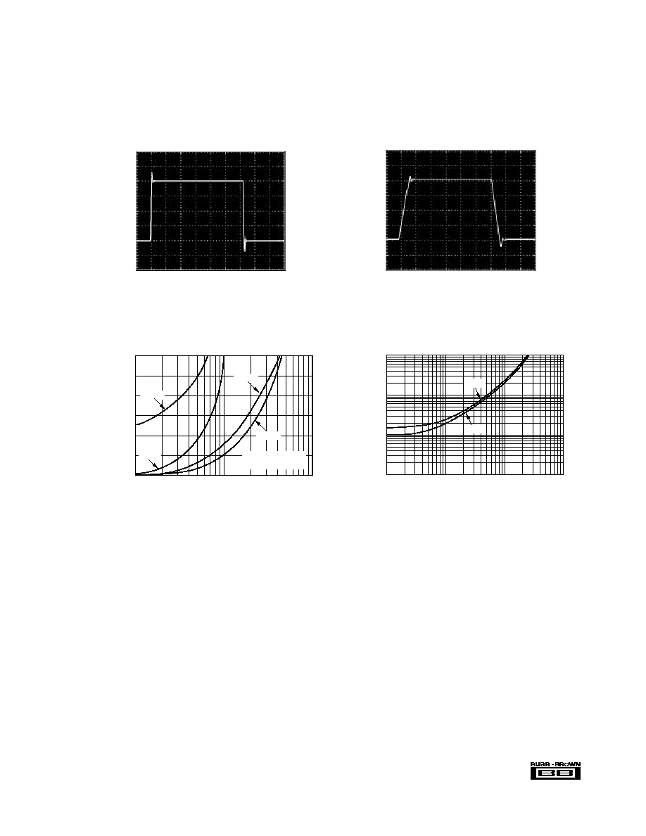
SMALL-SIGNAL STEP RESPONSE
C
L
= 100pF
1
µ
s/div
50mV/div
1
µ
s/div
LARGE-SIGNAL STEP RESPONSE
C
L
= 100pF
1V/div
SMALL-SIGNAL OVERSHOOT vs LOAD CAPACITANCE
10k
1000
Load Capacitance (pF)
100
60
50
40
30
20
10
0
Overshoot (%)
G = +1
G = ≠1
G = ≠5
See text for
reducing overshoot.
G = +5
SETTLING TIME vs CLOSED-LOOP GAIN
100
10
1
0.1
Settling Time (µs)
Closed-Loop Gain (V/V)
1
10
100
1000
0.1%
0.01%

8
Æ
OPA340/2340/4340
APPLICATIONS INFORMATION
OPA340 series op amps are fabricated on a state-of-the-art
0.6 micron CMOS process. They are unity-gain stable and
suitable for a wide range of general purpose applications.
Rail-to-rail input/output make them ideal for driving sam-
pling A/D converters. In addition, excellent ac performance
makes them well-suited for audio applications. The class AB
output stage is capable of driving 600
loads connected to
any point between V+ and ground.
Rail-to-rail input and output swing significantly increases
dynamic range, especially in low supply applications.
Figure 1 shows the input and output waveforms for the
OPA340 in unity-gain configuration. Operation is from a
single +5V supply with a 10k
load connected to V
S
/2.
The input is a 5Vp-p sinusoid. Output voltage is approxi-
mately 4.98Vp-p.
Power supply pins should be bypassed with 0.01
µ
F ceramic
capacitors.
OPERATING VOLTAGE
OPA340 series op amps are fully specified from +2.7V to
+5V. However, supply voltage may range from +2.5V to
+5.5V. Parameters are guaranteed over the specified supply
range--a unique feature of the OPA340 series. In addition,
many specifications apply from ≠40
∞
C to +85
∞
C. Most
behavior remains virtually unchanged throughout the full
operating voltage range. Parameters which vary signifi-
cantly with operating voltages or temperature are shown in
the typical performance curves.
RAIL-TO-RAIL INPUT
The input common-mode voltage range of the OPA340
series extends 500mV beyond the supply rails. This is
achieved with a complementary input stage--an N-channel
input differential pair in parallel with a P-channel differen-
tial pair (see Figure 2). The N-channel pair is active for input
voltages close to the positive rail, typically
(V+) ≠1.3V to 500mV above the positive supply, while the
P-channel pair is on for inputs from 500mV below the
negative supply to approximately (V+) ≠1.3V. There is a
small transition region, typically (V+) ≠1.5V to (V+) ≠1.1V,
in which both pairs are on. This 400mV transition region
can vary
±
300mV with process variation. Thus, the transi-
tion region (both stages on) can range from (V+) ≠1.8V to
(V+) ≠1.4V on the low end, up to (V+) ≠1.2V to (V+) ≠0.8V
on the high end.
FIGURE 2. Simplified Schematic.
V
S
= +5, G = +1, R
L
= 10k
V
IN
2V/div
FIGURE 1. Rail-to-Rail Input and Output.
V
BIAS1
V
BIAS2
V
IN
+
V
IN
≠
Class AB
Control
Circuitry
V
O
V≠
(Ground)
V+
Reference
Current
5
5
0
V
OUT

9
Æ
OPA340/2340/4340
OPA340 series op amps are laser-trimmed to the reduce
offset voltage difference between the N-channel and
P-channel input stages, resulting in improved common-
mode rejection and a smooth transition between the
N-channel pair and the P-channel pair. However, within the
400mV transition region PSRR, CMRR, offset voltage,
offset drift, and THD may be degraded compared to opera-
tion outside this region.
A double-folded cascode adds the signal from the two input
pairs and presents a differential signal to the class AB output
stage. Normally, input bias current is approximately 200fA,
however, input voltages exceeding the power supplies by
more than 500mV can cause excessive current to flow in or
out of the input pins. Momentary voltages greater than
500mV beyond the power supply can be tolerated if the
current on the input pins is limited to 10mA. This is easily
accomplished with an input resistor as shown in Figure 3.
Many input signals are inherently current-limited to less
than 10mA, therefore, a limiting resistor is not required.
CAPACITIVE LOAD AND STABILITY
OPA340 series op amps can drive a wide range of capacitive
loads. However, all op amps under certain conditions may
become unstable. Op amp configuration, gain, and load
value are just a few of the factors to consider when determin-
ing stability. An op amp in unity gain configuration is the
most susceptible to the effects of capacitive load. The
capacitive load reacts with the op amp's output resistance,
along with any additional load resistance, to create a pole in
the small-signal response which degrades the phase margin.
In unity gain, OPA340 series op amps perform well, with a
pure capacitive load up to approximately 1000pF. Increasing
gain enhances the amplifier's ability to drive more capaci-
tance. See the typical performance curve "Small-Signal
Overshoot vs Capacitive Load."
One method of improving capacitive load drive in the unity
gain configuration is to insert a 10
to 20
resistor in series
with the output, as shown in Figure 4. This significantly
reduces ringing with large capacitive loads. However, if
there is a resistive load in parallel with the capacitive load,
it creates a voltage divider introducing a dc error at the
output and slightly reduces output swing. This error may be
insignificant. For instance, with R
L
= 10k
and R
S
= 20
,
there is only about a 0.2% error at the output.
DRIVING A/D CONVERTERS
OPA340 series op amps are optimized for driving medium
speed (up to 100kHz) sampling A/D converters. However,
they also offer excellent performance for higher speed
converters. The OPA340 series provides an effective means
of buffering the A/D's input capacitance and resulting
charge injection while providing signal gain.
Figures 5 and 6 show the OPA340 driving an ADS7816.
The ADS7816 is a 12-bit, micro-power sampling converter
in the tiny MSOP-8 package. When used with the minia-
ture package options of the OPA340 series, the combina-
tion is ideal for space-limited and low power applications.
For further information consult the ADS7816 data sheet.
With the OPA340 in a noninverting configuration, an RC
network at the amplifier's output can be used to filter high
frequency noise in the signal (Figure 5). In the inverting
configuration, filtering may be accomplished with a ca-
pacitor across the feedback resistor (Figure 6).
FIGURE 3. Input Current Protection for Voltages Exceeding
the Supply Voltage.
5k
OPAx340
10mA max
V+
V
IN
V
OUT
I
OVERLOAD
RAIL-TO-RAIL OUTPUT
A class AB output stage with common-source transistors is
used to achieve rail-to-rail output. For light resistive loads
(>50k
), the output voltage is typically a few millivolts
from the supply rails. With moderate resistive loads (2k
to
50k
), the output can swing to within a few tens of milli-
volts from the supply rails and maintain high open-loop
gain. See the typical performanc curve "Output Voltage
Swing vs Output Current."
FIGURE 4. Series Resistor in Unity-Gain Configuration Improves Capacitive Load Drive.
10
to
20
OPAx340
V+
V
IN
V
OUT
R
S
R
L
C
L

10
Æ
OPA340/2340/4340
FIGURE 5. OPA340 in Noninverting Configuration Driving ADS7816.
FIGURE 6. OPA340 in Inverting Configuration Driving ADS7816.
FIGURE 7. Speech Bandpass Filter.
ADS7816
12-Bit A/D
DCLOCK
D
OUT
CS/SHDN
OPA340
+5V
V
IN
V+
2
+In
3
≠In
V
REF
8
4
GND
Serial
Interface
1
0.1µF
0.1µF
7
6
5
NOTE: A/D Input = 0 to V
REF
5k
5k
330pF
V
IN
= 0V to ≠5V for 0V to 5V output.
ADS7816
12-Bit A/D
DCLOCK
D
OUT
CS/SHDN
OPA340
+5V
V
IN
V+
2
+In
3
≠In
V
REF
8
4
GND
Serial
Interface
1
0.1µF
0.1µF
7
6
5
NOTE: A/D Input = 0 to V
REF
V
IN
= 0V to 5V for
0V to 5V output.
RC network filters high frequency noise.
500
3300pF
243k
10M
10M
1.74M
220pF
47pF
200pF
1/2
OPA2340
+5V
V
IN
R
L
1/2
OPA2340
Filters 160Hz to 2.4kHz