
SBOS212A ≠ NOVEMBER, 2001
www.ti.com
DESCRIPTION
The OPAx356 series high-speed, voltage-feedback CMOS
operational amplifiers are designed for video and other
applications requiring wide bandwidth. The OPAx356 is unity
gain stable and can drive large output currents. Differential
gain is 0.02% and differential phase is 0.05
∞
. Quiescent
current is only 8.3mA per channel.
OPAx356 is optimized for operation on single or dual sup-
plies as low as 2.5V (
±
1.25V) and up to 5.5V (
±
2.75V).
Common-mode input range for the OPAx356 extends 100mV
below ground and up to 1.5V from V+. The output swing is
within 100mV of the rails, supporting wide dynamic range.
The OPAx356 series is available in single (SOT23-5 and SO-8),
and dual (MSOP-8 and SO-8) versions. Multichannel versions
feature completely independent circuitry for lowest crosstalk and
freedom from interaction. All are specified over the extended
≠40
∞
C to +125
∞
C range.
FEATURES
q
UNITY-GAIN BANDWIDTH: 450MHz
q
WIDE BANDWIDTH: 200MHz GBW
q
HIGH SLEW RATE: 360V/
µ
s
q
LOW NOISE: 5.8nV/
Hz
q
EXCELLENT VIDEO PERFORMANCE:
DIFF GAIN: 0.02%, DIFF PHASE: 0.05
∞
0.1dB GAIN FLATNESS: 75MHz
q
INPUT RANGE INCLUDES GROUND
q
RAIL-TO-RAIL OUTPUT (within 100mV)
q
LOW INPUT BIAS CURRENT: 3pA
q
THERMAL SHUTDOWN
q
SINGLE-SUPPLY OPERATING RANGE: 2.5V to 5.5V
q
MicroSIZE PACKAGES
PRODUCTION DATA information is current as of publication date.
Products conform to specifications per the terms of Texas Instruments
standard warranty. Production processing does not necessarily include
testing of all parameters.
Copyright © 2001, Texas Instruments Incorporated
200MHz, CMOS
OPERATIONAL AMPLIFIER
Please be aware that an important notice concerning availability, standard warranty, and use in critical applications of
Texas Instruments semiconductor products and disclaimers thereto appears at the end of this data sheet.
APPLICATIONS
q
VIDEO PROCESSING
q
ULTRASOUND
q
OPTICAL NETWORKING, TUNABLE LASERS
q
PHOTODIODE TRANSIMPEDANCE AMPS
q
ACTIVE FILTERS
q
HIGH-SPEED INTEGRATORS
q
ANALOG-TO-DIGITAL (A/D) CONVERTER
INPUT BUFFERS
q
DIGITAL-TO-ANALOG (D/A) CONVERTER
OUTPUT AMPLIFIERS
q
BARCODE SCANNERS
q
COMMUNICATIONS
OPAx356 RELATED PRODUCTS
FEATURES
PRODUCT
200MHz, Rail-to-Rail Output, CMOS, Shutdown
OPAx355
38MHz, Rail-to-Rail Input/Output, CMOS
OPAx350
75MHz, Rail-to-Rail Output
OPAx631
150MHz, Rail-to-Rail Output
OPAx634
Differential Input/Output, 3.3V Supply
THS412x
OPA356
Out
V+
V≠
≠V
IN
+V
IN
OPA3
56
OPA2
356
OPA2
356
OPA356
OPA2356

OPA356, 2356
2
SBOS212A
ABSOLUTE MAXIMUM RATINGS
(1)
Supply Voltage, V+ to V≠ ................................................................... 7.5V
Signal Input Terminals, Voltage
(2)
.................... (V≠) ≠ 0.5V to (V+) + 0.5V
Current
(2)
..................................................... 10mA
Output Short-Circuit
(3)
.............................................................. Continuous
Operating Temperature .................................................. ≠55
∞
C to +150
∞
C
Storage Temperature ...................................................... ≠65
∞
C to +150
∞
C
Junction Temperature .................................................................... +160
∞
C
Lead Temperature (soldering, 10s) ............................................... +300
∞
C
NOTE: (1) Stresses above these ratings may cause permanent damage.
Exposure to absolute maximum conditions for extended periods may degrade
device reliability. These are stress ratings only, and functional operation of the
device at these or any other conditions beyond those specified is not implied.
(2) Input terminals are diode-clamped to the power-supply rails. Input signals
that can swing more than 0.5V beyond the supply rails should be current limited
to 10mA or less. (3) Short-circuit to ground one amplifier per package.
ELECTROSTATIC
DISCHARGE SENSITIVITY
This integrated circuit can be damaged by ESD. Texas Instru-
ments recommends that all integrated circuits be handled with
appropriate precautions. Failure to observe proper handling
and installation procedures can cause damage.
ESD damage can range from subtle performance degradation
to complete device failure. Precision integrated circuits may be
more susceptible to damage because very small parametric
changes could cause the device not to meet its published
specifications.
PACKAGE/ORDERING INFORMATION
Top View
PIN CONFIGURATIONS
1
2
3
5
4
V+
≠In
Out
V≠
+In
OPA356
SOT23
1
2
3
4
8
7
6
5
NC
(1)
V+
Out
NC
(1)
NC
(1)
≠In
+In
V≠
OPA356
SO
1
2
3
4
8
7
6
5
V+
Out B
≠In B
+In B
Out A
≠In A
+In A
V≠
OPA2356
MSOP, SO
A
B
NOTE: (1) NC means no internal connection.
SPECIFIED
PACKAGE
TEMPERATURE
PACKAGE
ORDERING
TRANSPORT
PRODUCT
PACKAGE-LEAD
DESIGNATOR
(1)
RANGE
MARKING
NUMBER
(2)
MEDIA, QUANTITY
OPA356AIDBV
SOT23-5
DBV
≠40
∞
C to +125
∞
C
OAAI
OPA356AIDBVT
Tape and Reel, 250
"
"
"
"
"
OPA356AIDBVR
Tape and Reel, 3000
OPA356AID
SO-8
D
≠40
∞
C to +125
∞
C
OPA356A
OPA356AID
Rails, 100
"
"
"
"
"
OPA356AIDR
Tape and Reel, 2500
OPA2356AIDGK
MSOP-8
DGK
≠40
∞
C to +125
∞
C
AYI
OPA2356AIDGKT
Tape and Reel, 250
"
"
"
"
"
OPA2356AIDGKR
Tape and Reel, 2500
OPA2356AID
SO-8
D
≠40
∞
C to +125
∞
C
OPA2356A
OPA2356AID
Rails, 100
"
"
"
"
"
OPA2356AIDR
Tape and Reel, 2500
NOTES: (1) For the most current specifications and package information, refer to our web site at www.ti.com. (2) Models labeled with "T" indicate smaller quantity
tape and reel, "R" indicates large quantity tape and reel and "D" indicates rails of specified quantity.
OPA356, 2356
3
SBOS212A
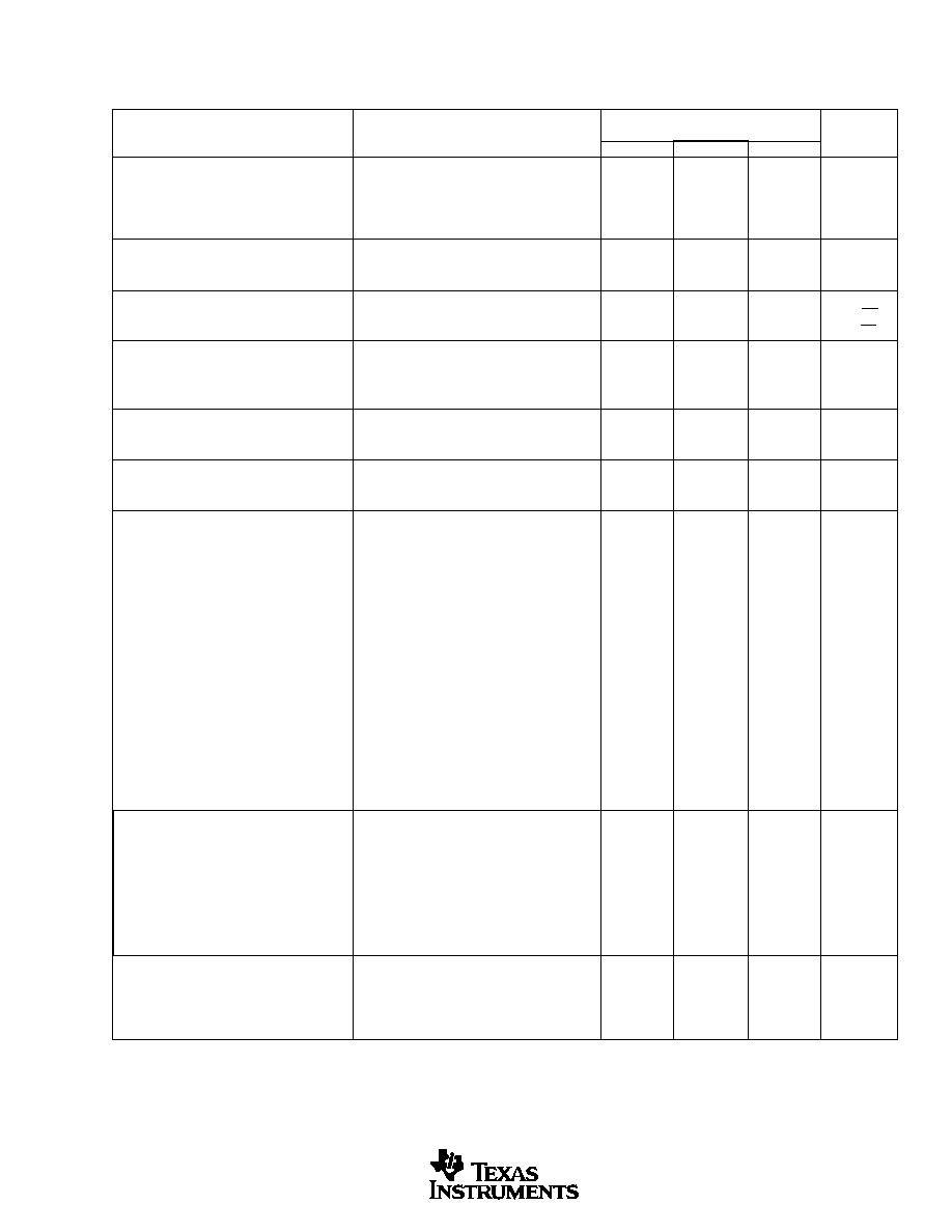
ELECTRICAL CHARACTERISTICS:
V
S
= +2.7V to +5.5V Single Supply
Boldface limits apply over the specified temperature range, T
A
= ≠40
∞
C to +125
∞
C.
At T
A
= +25
∞
C, R
F
= 604
, R
L
= 150
, Connected to V
S
/2, unless otherwise noted.
OPA356AIDBV, AID,
OPA2356AIDGK, AID
PARAMETER
CONDITION
MIN
TYP
MAX
UNITS
OFFSET VOLTAGE
Input Offset Voltage
V
OS
V
S
= +5V
±
2
±
9
mV
Specified Temperature Range
±
15
mV
vs Temperature
dV
OS
/dT
Specified Temperature Range
±
7
µ
V/
∞
C
vs Power Supply
PSRR
V
S
= +2.7V to +5.5V, V
CM
= V
S
/2 ≠ 0.15V
±
80
±
350
µ
V/V
INPUT BIAS CURRENT
Input Bias Current
I
B
3
±
50
pA
Input Offset Current
I
OS
±
1
±
50
pA
NOISE
Input Noise Voltage Density
e
n
f = 1MHz
5.8
nV/
Hz
Current Noise Density
i
n
f = 1MHz
50
fA/
Hz
INPUT VOLTAGE RANGE
Common-Mode Voltage Range
V
CM
(V≠) ≠ 0.1
(V+) ≠ 1.5
V
Common-Mode Rejection Ratio
CMRR
V
S
= +5.5V, ≠0.1V < V
CM
< +4.0V
66
80
dB
Specified Temperature Range
66
dB
INPUT IMPEDANCE
Differential
10
13
|| 1.5
|| pF
Common-Mode
10
13
|| 1.5
|| pF
OPEN-LOOP GAIN
V
S
= +5V, 0.3V < V
O
< 4.7V
84
92
dB
OPA356
V
S
= +5V, 0.3V < V
O
< 4.7V
80
dB
OPA2356
V
S
= +5V, 0.4V < V
O
< 4.6V
80
dB
FREQUENCY RESPONSE
Small-Signal Bandwidth
f
≠3dB
G = +1, V
O
= 100mVp-p, R
F
= 0
450
MHz
f
≠3dB
G = +2, V
O
= 100mVp-p, R
L
= 50
100
MHz
f
≠3dB
G = +2, V
O
= 100mVp-p, R
L
= 150
170
MHz
f
≠3dB
G = +2, V
O
= 100mVp-p, R
L
= 1k
200
MHz
Gain-Bandwidth Product
GBW
G = +10, R
L
= 1k
200
MHz
Bandwidth for 0.1dB Gain Flatness
f
0.1dB
G = +2, V
O
= 100mVp-p, R
F
= 560
75
MHz
Slew Rate
SR
V
S
= +5V, G = +2, 4V Output Step
300/≠360
V/
µ
s
Rise-and-Fall Time
G = +2, V
O
= 200mVp-p, 10% to 90%
2.4
ns
G = +2, V
O
= 2Vp-p, 10% to 90%
8
ns
Settling Time, 0.1%
V
S
= +5V, G = +2, 2V Output Step
30
ns
0.01%
V
S
= +5V, G = +2, 2V Output Step
120
ns
Overload Recovery Time
V
IN
∑ Gain = V
S
8
ns
Harmonic Distortion
2
nd
Harmonic
G = +2, f = 1MHz, V
O
= 2Vp-p, R
L
= 200
≠81
dBc
3
rd
Harmonic
G = +2, f = 1MHz, V
O
= 2Vp-p, R
L
= 200
≠93
dBc
Differential Gain Error
NTSC, R
L
= 150
0.02
%
Differential Phase Error
NTSC, R
L
= 150
0.05
degrees
Channel-to-Channel Crosstalk
OPA2356
f = 5MHz
≠90
dB
OUTPUT
Voltage Output Swing from Rail
V
S
= +5V, R
L
= 150
, A
OL
> 84dB
0.2
0.3
V
Voltage Output Swing from Rail
V
S
= +5V, R
L
= 1k
0.1
V
Voltage Output Swing from Rail
I
O
=
±
100mA
0.8
1
V
Ouput Current, Continuous
(1)
I
O
±
60
mA
Maximum Output Current, Peak
(1)
I
O
V
S
= +5V
±
100
mA
Maximum Output Current, Peak
(1)
I
O
V
S
= +3V
±
80
mA
Short Circuit Current
+250/ ≠200
mA
Closed-Loop Output Impedance
f < 100kHz
0.02
POWER SUPPLY
Specified Voltage Range
V
S
2.7
5.5
V
Operating Voltage Range
2.5 to 5.5
V
Quiescent Current (per amplifier)
I
Q
V
S
= +5V, I
O
= 0
8.3
11
mA
Specified Temperature Range
14
mA

OPA356, 2356
4
SBOS212A
ELECTRICAL CHARACTERISTICS:
V
S
= +2.7V to +5.5V Single Supply
(Cont.)
Boldface limits apply over the specified temperature range, T
A
= ≠40
∞
C to +125
∞
C.
At T
A
= +25
∞
C, R
F
= 604
, R
L
= 150
, Connected to V
S
/2, unless otherwise noted.
OPA356AIDBV, AID,
OPA2356AIDGK, AID
PARAMETER
CONDITION
MIN
TYP
MAX
UNITS
THERMAL SHUTDOWN
Junction Temperature
Shutdown
160
∞
C
Reset from Shutdown
140
∞
C
TEMPERATURE RANGE
Specified Range
≠40
125
∞
C
Operating Range
≠55
150
∞
C
Storage Range
≠65
150
∞
C
Thermal Resistance
JA
∞
C/W
SOT23-5, MSOP-8
150
∞
C/W
SO-8
125
∞
C/W
NOTES: (1) See typical characteristic "Output Voltage Swing vs Output Current".
OPA356, 2356
5
SBOS212A
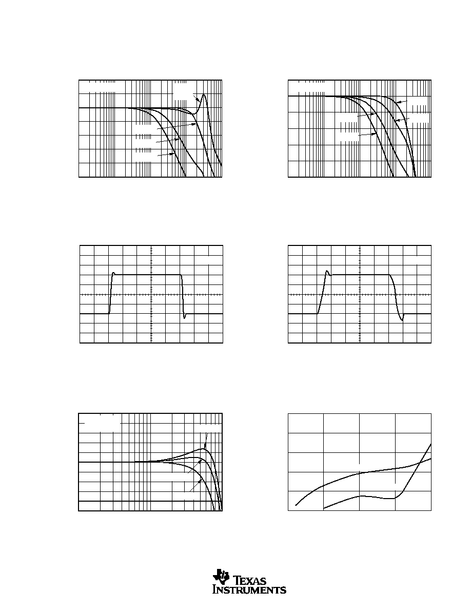
TYPICAL CHARACTERISTICS
At T
A
= +25
∞
C and V
S
= 5V, G = +2, R
F
= 604
, R
L
= 150
connected to V
S
/2, unless otherwise noted.
NON-INVERTING SMALL-SIGNAL
FREQUENCY RESPONSE
Frequency (Hz)
Normalized Gain (dB)
10M
1M
100M
1G
100k
6
3
0
≠3
≠6
≠9
≠12
≠15
V
O
= 0.1Vp-p
G = +2
G = +5
G = +10
G = +1
R
F
= 0
INVERTING SMALL-SIGNAL
FREQUENCY RESPONSE
Frequency (Hz)
Normalized Gain (dB)
10M
1M
100M
1G
100k
3
0
≠3
≠6
≠9
≠12
≠15
V
O
= 0.1Vp-p
G = ≠1
G = ≠5
G = ≠10
G = ≠2
NON-INVERTING SMALL-SIGNAL
STEP RESPONSE
Time (20ns/div)
Output V
oltage (50mV/div)
G = +2
NON-INVERTING LARGE-SIGNAL
STEP RESPONSE
Time (20ns/div)
Output V
oltage (500mV/div)
G = +2
0.1dB GAIN FLATNESS FOR VARIOUS R
F
Frequency (MHz)
Normalized Gain (dB)
10
100
1
0.5
0.4
0.3
0.2
0.1
0
≠0.1
≠0.2
≠0.3
≠0.4
≠0.5
V
O
= 0.1Vp-p
C
L
= 0pF
R
F
= 604
R
F
= 560
R
F
= 500
HARMONIC DISTORTION vs OUTPUT VOLTAGE
Output Voltage (Vp-p)
Harmonic Distortion (dBc)
2
3
4
0
1
≠50
≠60
≠70
≠80
≠90
≠100
R
L
= 200
f = 1MHz
2nd Harmonic
3rd Harmonic
OPA356, 2356
6
SBOS212A
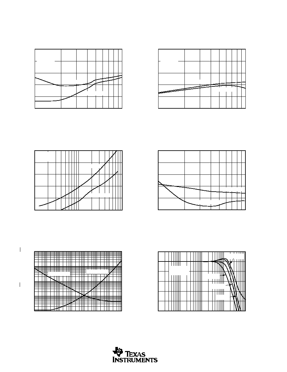
TYPICAL CHARACTERISTICS
(Cont.)
At T
A
= +25
∞
C and V
S
= 5V, G = +2, R
F
= 604
, R
L
= 150
connected to V
S
/2, unless otherwise noted.
HARMONIC DISTORTION vs NON-INVERTING GAIN
Gain (V/V)
Harmonic Distortion (dBc)
10
1
≠50
≠60
≠70
≠80
≠90
≠100
2nd Harmonic
3rd Harmonic
V
O
= 2Vp-p
f = 1MHz
R
L
= 200
HARMONIC DISTORTION vs INVERTING GAIN
Gain (V/V)
Harmonic Distortion (dBc)
10
1
≠50
≠60
≠70
≠80
≠90
≠100
2nd Harmonic
3rd Harmonic
V
O
= 2Vp-p
f = 1MHz
R
L
= 200
HARMONIC DISTORTION vs FREQUENCY
Frequency (Hz)
Harmonic Distortion (dBc)
10M
100k
1M
≠50
≠60
≠70
≠80
≠90
≠100
2nd Harmonic
3rd Harmonic
V
O
= 2Vp-p
R
L
= 200
HARMONIC DISTORTION vs LOAD RESISTANCE
R
L
(
)
Harmonic Distortion (dBc)
1k
100
≠50
≠60
≠70
≠80
≠90
≠100
2nd Harmonic
3rd Harmonic
V
O
= 2Vp-p
f = 1MHz
INPUT VOLTAGE AND CURRENT NOISE
SPECTRAL DENSITY vs FREQUENCY
Frequency (Hz)
V
oltage Noise (nV/
Hz), Current Noise (fA/
Hz)
100M
10
100
1k
10k
100k
1M
10M
10k
1k
100
10
1
Current Noise
Voltage Noise
FREQUENCY RESPONSE FOR VARIOUS R
L
Frequency (Hz)
Normalized Gain (dB)
10M
1M
100M
1G
100k
3
0
≠3
≠6
≠9
≠12
≠15
R
L
= 50
R
L
= 150
R
L
= 1k
R
L
= 10k
C
L
= 0pF
V
O
= 0.1Vp-p
OPA356, 2356
7
SBOS212A
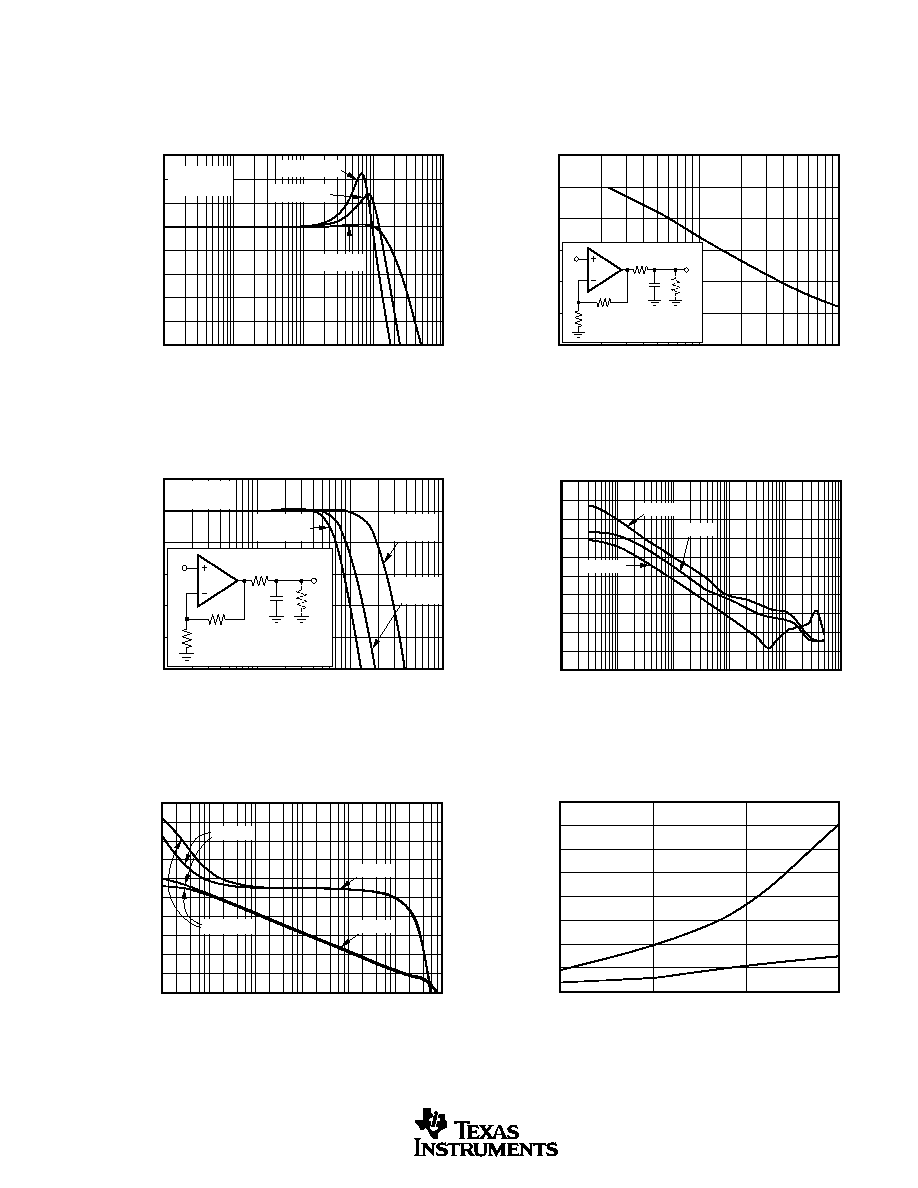
TYPICAL CHARACTERISTICS
(Cont.)
At T
A
= +25
∞
C and V
S
= 5V, G = +2, R
F
= 604
, R
L
= 150
connected to V
S
/2, unless otherwise noted.
FREQUENCY RESPONSE FOR VARIOUS C
L
Frequency (Hz)
Normalized Gain (dB)
10M
1M
100M
1G
100k
9
6
3
0
≠3
≠6
≠9
≠12
≠15
R
S
= 0
V
O
= 0.1Vp-p
C
L
= 100pF
C
L
= 47pF
C
L
= 5.6pF
RECOMMENDED R
S
vs CAPACITIVE LOAD
Capacitive Load (pF)
R
S
(
)
10
100
1
120
100
80
60
40
20
0
OPA356
C
L
R
S
V
IN
V
O
1k
604
604
(1k
is
Optional)
FREQUENCY RESPONSE vs CAPACITIVE LOAD
Frequency (Hz)
Normalized Gain (dB)
10M
100M
1G
1M
3
0
≠3
≠6
≠9
≠12
≠15
C
L
= 100pF
R
S
= 24
C
L
= 47pF
R
S
= 36
C
L
= 5.6pF
R
S
= 80
OPA356
C
L
R
S
V
IN
V
O
1k
604
604
(1k
is
Optional)
G = +2
V
O
= 0.1Vp-p
Frequency (Hz)
10M
100M
100k
1M
1G
10k
100
90
80
70
60
50
40
30
20
10
0
≠PSRR
+PSRR
CMRR
COMMON-MODE REJECTION RATIO AND
POWER-SUPPLY REJECTION RATIO vs FREQUENCY
CMRR, PSRR (dB)
OPEN-LOOP GAIN AND PHASE
Frequency (Hz)
Open-Loop Gain (dB)
Open-Loop Phase (degrees)
10M
100M
100k
1M
1G
1k
10k
180
160
140
120
100
80
60
40
20
0
≠20
Gain
R
L
= 1k
R
L
= 150
Phase
COMPOSITE VIDEO
DIFFERENTIAL GAIN AND PHASE
Number of 150
Loads
dG/dP
(%/degrees)
3
2
4
1
0.40
0.35
0.30
0.25
0.20
0.15
0.10
0.05
0
dP
dG

OPA356, 2356
8
SBOS212A
TYPICAL CHARACTERISTICS
(Cont.)
At T
A
= +25
∞
C and V
S
= 5V, G = +2, R
F
= 604
, R
L
= 150
connected to V
S
/2, unless otherwise noted.
INPUT BIAS CURRENT vs TEMPERATURE
Temperature (
∞
C)
Input Bias Current (pA)
65
85
105
5
25
45
135
125
≠55
≠35
≠15
10n
1n
100
10
1
OUTPUT VOLTAGE SWING vs OUTPUT CURRENT
FOR V
S
= 3V
Output Current (mA)
Output V
o
ltage
(V)
60
30
90
120
150
0
3
2
1
0
125
∞
C
125
∞
C
25
∞
C
25
∞
C
≠55
∞
C
≠55
∞
C
Continuous currents above
60mA are not recommended
SUPPLY CURRENT vs TEMPERATURE
Temperature (
∞
C)
Supply Current (mA)
65
85
105
5
25
45
135
125
≠55
≠35
≠15
14
12
10
8
6
4
2
0
V
S
= 5V
V
S
= 3V
V
S
= 5.5V
V
S
= 2.5V
OUTPUT VOLTAGE SWING vs OUTPUT CURRENT
FOR V
S
= 5V
Output Current (mA)
Output V
o
ltage
(V)
100
50
150
200
250
0
5
4
3
2
1
0
125
∞
C
125
∞
C
25
∞
C
25
∞
C
≠55
∞
C
≠55
∞
C
Continuous currents above
60mA are not recommended
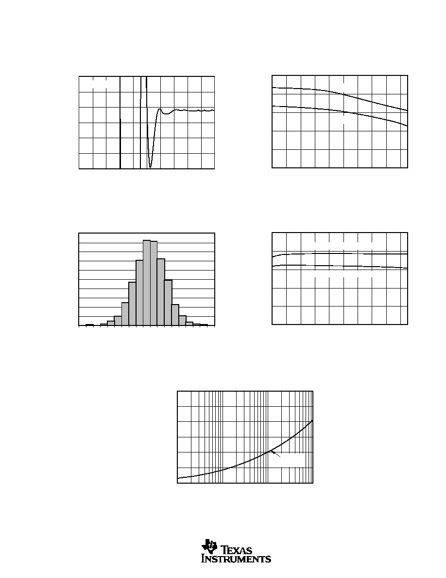
CLOSED-LOOP OUTPUT IMPEDANCE vs FREQUENCY
Frequency (Hz)
Output Impedance (
)
10M
100M
1M
1G
10k
100k
100
10
1
0.1
0.01
0.001
OPA356
604
604
Z
O
MAXIMUM OUTPUT VOLTAGE vs FREQUENCY
Frequency (MHz)
Output V
oltage (Vp-p)
10
100
1
6
5
4
3
2
1
0
V
S
= 5.5V
V
S
= 2.7V
Maximum Output
Voltage without
Slew-Rate
Induced Distortion
OPA356, 2356
9
SBOS212A
TYPICAL CHARACTERISTICS
(Cont.)
At T
A
= +25
∞
C and V
S
= 5V, G = +2, R
F
= 604
, R
L
= 150
connected to V
S
/2, unless otherwise noted.
OUTPUT SETTLING TIME TO 0.1%
Time (ns)
Output Error (%)
25
30
40
45
35
10
5
15
20
50
0
0.2
0.1
0
≠0.1
≠0.2
≠0.3
≠0.4
V
O
= 2Vp-p
OPEN-LOOP GAIN vs TEMPERATURE
Temperature (
∞
C)
Open-Loop Gain (dB)
65
85
105
5
25
45
135
125
≠55
≠35
≠15
110
100
90
80
70
60
R
L
= 1k
R
L
= 150
OFFSET VOLTAGE PRODUCTION DISTRIBUTION
Offset Voltage (mV)
Percent of
Amplifiers (%)
≠6
≠7
≠8
≠9
≠5 ≠4 ≠3 ≠2 ≠1 0 1
2 3 4 5 6 7 8 9
20
18
16
14
12
10
8
6
4
2
0
COMMON-MODE REJECTION RATIO AND
POWER-SUPPLY REJECTION RATIO vs TEMPERATURE
Temperature (
∞
C)
CMRR, PSRR (dB)
65
85
105
5
25
45
135
125
≠55
≠35
≠15
100
90
80
70
60
50
Power-Supply Rejection Ratio
Common-Mode Rejection Ratio
CHANNEL-TO-CHANNEL CROSSTALK
Frequency (Hz)
Crosstalk, Input-Referred (dB)
10M
1M
100M
100k
0
≠20
≠40
≠60
≠80
≠100
≠120
OPA2356
(dual)

OPA356, 2356
10
SBOS212A
APPLICATIONS INFORMATION
The OPAx356 series is a CMOS, high-speed, voltage feed-
back, operational amplifier designed for video and other
general-purpose applications. It is available as a single or
dual op amp.
The amplifier features a 200MHz gain bandwidth and
360V/
µ
s slew rate, but it is unity-gain stable and can be
operated as a +1V/V voltage follower.
Its input common-mode voltage range includes ground, al-
lowing the OPAx356 to be used in virtually any single-supply
application up to a supply voltage of +5.5V.
PCB LAYOUT
Good high-frequency PC board layout techniques should be
employed for the OPAx356. Generous use of ground planes,
short direct signal traces, and a suitable bypass capacitor
located at the V+ pin will assure clean, stable operation.
Large areas of copper also provide a means of dissipating
heat that is generated within the amplifier in normal opera-
tion.
Sockets are definitely not recommended for use with any
high-speed amplifier.
A 10
µ
F ceramic bypass capacitor is the minimum recom-
mended value; adding a 1
µ
F or larger tantalum capacitor in
parallel can be beneficial when driving a low-resistance load.
Providing adequate bypass capacitance is essential to achiev-
ing very low harmonic and intermodulation distortion.
OPERATING VOLTAGE
The OPAx356 is specified over a power-supply range of
+2.7V to +5.5V (
±
1.35 to
±
2.75V). However, the supply
voltage may range from +2.5V to +5.5V (
±
1.25V to
±
2.75V).
Supply voltages higher than 7.5V (absolute maximum) can
permanently damage the amplifier.
FIGURE 1. Internal ESD Protection.
Parameters that vary significantly over supply voltage or
temperature are shown in the "Typical Characteristics" sec-
tion of this data sheet.
OUTPUT DRIVE
The OPAx356 output stage is capable of driving a standard
back-terminated 75
video cable. By back-terminating a
transmission line, it does not exhibit a capacitive load to its
driver. A properly back-terminated 75
cable does not ap-
pear as capacitance; it presents only a 150
resistive load to
the OPAx356 output.
The output stage can supply high short-circuit current (typi-
cally over 200mA). Therefore, an on-chip thermal shutdown
circuit is provided to protect the OPAx356 from dangerously
high junction temperatures. At 160
∞
C, the protection circuit
will shut down the amplifier. Normal operation will resume
when the junction temperature cools to below 140
∞
C.
NOTE: It is not recommended to run a continuous DC current
in excess of
±
60mA. Refer to the graph of "Output Voltage
Swing vs Output Current", shown in the "Typical Character-
istics" section of this data sheet.
INPUT AND ESD PROTECTION
All OPAx356 pins are static protected with internal ESD
protection diodes tied to the supplies, as shown in Figure 1.
These diodes will provide overdrive protection if the current
is externally limited to 10mA by the source or by a resistor.
External
Pin
+V
CC
≠V
CC
Internal
Circuitry
OPA356, 2356
11
SBOS212A
PACKAGE DRAWINGS
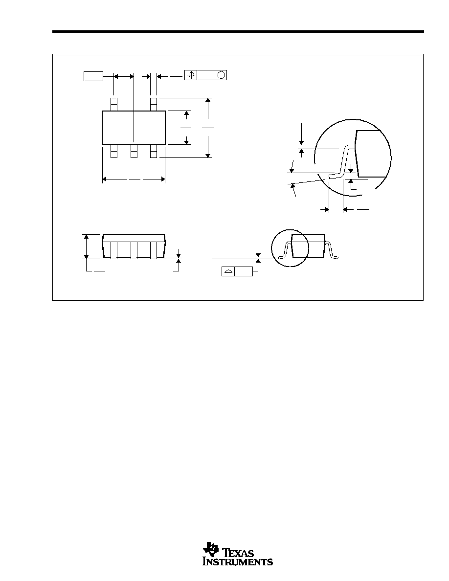
MPDS018D ≠ FEBRUARY 1996 ≠ REVISED JANUARY 2001
DBV (R-PDSO-G5)
PLASTIC SMALL-OUTLINE
0,10
M
0,20
0,95
0
∞
≠8
∞
0,25
0,35
0,55
Gage Plane
0,15 NOM
4073253-4/F 10/00
2,60
3,00
0,50
0,30
1,50
1,70
4
5
3
1
2,80
3,00
0,95
1,45
0,05 MIN
Seating Plane
NOTES: A. All linear dimensions are in millimeters.
B. This drawing is subject to change without notice.
C. Body dimensions do not include mold flash or protrusion.
D. Falls within JEDEC MO-178

OPA356, 2356
12
SBOS212A
PACKAGE DRAWINGS
(Cont.)
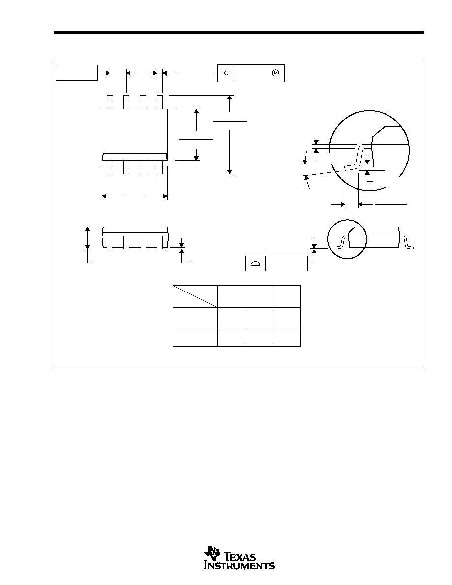
MPDS028B ≠ JUNE 1997 ≠ REVISED SEPTEMBER 2001
DGK (R-PDSO-G8)
PLASTIC SMALL-OUTLINE PACKAGE
0,69
0,41
0,25
0,15 NOM
Gage Plane
4073329/C 08/01
4,98
0,25
5
3,05
4,78
2,95
8
4
3,05
2,95
1
0,38
1,07 MAX
Seating Plane
0,65
M
0,08
0
∞
≠ 6
∞
0,10
0,15
0,05
NOTES: A. All linear dimensions are in millimeters.
B. This drawing is subject to change without notice.
C. Body dimensions do not include mold flash or protrusion.
D. Falls within JEDEC MO-187
OPA356, 2356
13
SBOS212A
PACKAGE DRAWINGS
(Cont.)
MSOI002B ≠ JANUARY 1995 ≠ REVISED SEPTEMBER 2001
D (R-PDSO-G**)
PLASTIC SMALL-OUTLINE PACKAGE
8 PINS SHOWN
8
0.197
(5,00)
A MAX
A MIN
(4,80)
0.189
0.337
(8,55)
(8,75)
0.344
14
0.386
(9,80)
(10,00)
0.394
16
DIM
PINS **
4040047/E 09/01
0.069 (1,75) MAX
Seating Plane
0.004 (0,10)
0.010 (0,25)
0.010 (0,25)
0.016 (0,40)
0.044 (1,12)
0.244 (6,20)
0.228 (5,80)
0.020 (0,51)
0.014 (0,35)
1
4
8
5
0.150 (3,81)
0.157 (4,00)
0.008 (0,20) NOM
0
∞
≠ 8
∞
Gage Plane
A
0.004 (0,10)
0.010 (0,25)
0.050 (1,27)
NOTES: A. All linear dimensions are in inches (millimeters).
B. This drawing is subject to change without notice.
C. Body dimensions do not include mold flash or protrusion, not to exceed 0.006 (0,15).
D. Falls within JEDEC MS-012
PACKAGING INFORMATION
ORDERABLE DEVICE
STATUS(1)
PACKAGE TYPE
PACKAGE DRAWING
PINS
PACKAGE QTY
OPA2356AID
ACTIVE
SOIC
D
8
100
OPA2356AIDGKR
ACTIVE
VSSOP
DGK
8
2500
OPA2356AIDGKT
ACTIVE
VSSOP
DGK
8
250
OPA2356AIDR
ACTIVE
SOIC
D
8
2500
OPA356AID
ACTIVE
SOIC
D
8
100
OPA356AIDBVR
ACTIVE
SOP
DBV
5
3000
OPA356AIDBVT
ACTIVE
SOP
DBV
5
250
OPA356AIDR
ACTIVE
SOIC
D
8
2500
(1) The marketing status values are defined as follows:
ACTIVE: Product device recommended for new designs.
LIFEBUY: TI has announced that the device will be discontinued, and a lifetime-buy period is in effect.
NRND: Not recommended for new designs. Device is in production to support existing customers, but TI does not recommend using this part in
a new design.
PREVIEW: Device has been announced but is not in production. Samples may or may not be available.
OBSOLETE: TI has discontinued the production of the device.
PACKAGE OPTION ADDENDUM
www.ti.com
3-Oct-2003

IMPORTANT NOTICE
Texas Instruments Incorporated and its subsidiaries (TI) reserve the right to make corrections, modifications,
enhancements, improvements, and other changes to its products and services at any time and to discontinue
any product or service without notice. Customers should obtain the latest relevant information before placing
orders and should verify that such information is current and complete. All products are sold subject to TI's terms
and conditions of sale supplied at the time of order acknowledgment.
TI warrants performance of its hardware products to the specifications applicable at the time of sale in
accordance with TI's standard warranty. Testing and other quality control techniques are used to the extent TI
deems necessary to support this warranty. Except where mandated by government requirements, testing of all
parameters of each product is not necessarily performed.
TI assumes no liability for applications assistance or customer product design. Customers are responsible for
their products and applications using TI components. To minimize the risks associated with customer products
and applications, customers should provide adequate design and operating safeguards.
TI does not warrant or represent that any license, either express or implied, is granted under any TI patent right,
copyright, mask work right, or other TI intellectual property right relating to any combination, machine, or process
in which TI products or services are used. Information published by TI regarding third-party products or services
does not constitute a license from TI to use such products or services or a warranty or endorsement thereof.
Use of such information may require a license from a third party under the patents or other intellectual property
of the third party, or a license from TI under the patents or other intellectual property of TI.
Reproduction of information in TI data books or data sheets is permissible only if reproduction is without
alteration and is accompanied by all associated warranties, conditions, limitations, and notices. Reproduction
of this information with alteration is an unfair and deceptive business practice. TI is not responsible or liable for
such altered documentation.
Resale of TI products or services with statements different from or beyond the parameters stated by TI for that
product or service voids all express and any implied warranties for the associated TI product or service and
is an unfair and deceptive business practice. TI is not responsible or liable for any such statements.
Following are URLs where you can obtain information on other Texas Instruments products and application
solutions:
Products
Applications
Amplifiers
amplifier.ti.com
Audio
www.ti.com/audio
Data Converters
dataconverter.ti.com
Automotive
www.ti.com/automotive
DSP
dsp.ti.com
Broadband
www.ti.com/broadband
Interface
interface.ti.com
Digital Control
www.ti.com/digitalcontrol
Logic
logic.ti.com
Military
www.ti.com/military
Power Mgmt
power.ti.com
Optical Networking
www.ti.com/opticalnetwork
Microcontrollers
microcontroller.ti.com
Security
www.ti.com/security
Telephony
www.ti.com/telephony
Video & Imaging
www.ti.com/video
Wireless
www.ti.com/wireless
Mailing Address:
Texas Instruments
Post Office Box 655303 Dallas, Texas 75265
Copyright
2003, Texas Instruments Incorporated