Document Outline
- FEATURES
- APPLICATIONS
- DESCRIPTION
- RELATED LOW VOLTAGE VIDEO AMPS
- PRELIMINARY ORDERING INFORMATION(1)
- ABSOLUTE MAXIMUM RATINGS(1)
- PIN CONFIGURATION
- ELECTRICAL CHARACTERISTICS: VS = + 2.7V to + 3.3V Single- Supply
- TYPICAL CHARACTERISTICS: VS = 3.3V
- APPLICATIONS INFORMATION
- OPERATING VOLTAGE
- INPUT VOLTAGE
- INPUT OVERVOLTAGE PROTECTION
- ENABLE/SHUTDOWN
- INTERNAL 2-POLE FILTER
- VIDEO PERFORMANCE
- FREQUENCY RESPONSE OF THE OPA360
- INTERNAL LEVEL SHIFT
- OUTPUT SWING TO GND (SYNC PULSE)
- SAG CORRECTION
- SUPPLY VOLTAGE vs COUPLING CAPACITOR
- DC COUPLED OUTPUT
FEATURES
D
EXCELLENT VIDEO PERFORMANCE
D
INTERNAL GAIN: 6dB
D
2-POLE RECONSTRUCTION FILTER
D
SAG CORRECTION
- Reduces Coupling Capacitor Size
D
INPUT RANGE INCLUDES GROUND
- DC-Coupled Input
D
INTEGRATED LEVEL SHIFTER
- DC-Coupled Output
(1)
- No Output Capacitors Needed
D
RAIL-TO-RAIL OUTPUT
D
LOW QUIESCENT CURRENT: 6mA
D
SHUTDOWN CURRENT: 5
m
A
D
SINGLE-SUPPLY: 2.7V to 3.3V
D
SC70-6 PACKAGE: 2.0mm x 2.1mm
(1) Internal circuitry prevents the output from saturating, even with 0V sync
tip level at the input video signal.
APPLICATIONS
D
DIGITAL CAMERAS
D
CAMERA PHONES
D
SET-TOP-BOX VIDEO FILTERS
RELATED LOW VOLTAGE VIDEO AMPS
FEATURES
PRODUCT
2.7V to 5.5V, 200MHz GBW, 300V/
�
s, 6
�
A Sleep, SOT23
OPA355
2.7V to 5.5V, RRIO, 150V/
�
s, 5mA IQ, 6
�
A Sleep, SOT23
OPA357
2.7V to 3.3V, SC70, 70MHz, 6mA IQ, 5
�
A Sleep
OPA358(1)
2.7V to 3.3V, SC70, Filter, SAG, G = 12dB, 5
�
A Sleep
OPA361(1)
(1) Available Q4 2004.
DESCRIPTION
The OPA360 high-speed amplifier is optimized for 3V
portable video applications. It has been specifically
designed to be compatible with digital-to-analog
converters (DACs) embedded in video processors, such
as Texas Instruments' family of Digital Media Processors
and others. The input common-mode range includes
GND, which allows the Video-DAC to be DC-coupled to
the OPA360.
The output swings within 25mV of GND and 300mV to V+
with a standard back-terminated video load (150
). An
internal level shift circuit prevents the output from
saturating with 0V input, thus preventing sync-pulse
clipping in common video circuits. Therefore, the OPA360
is ideally suited for DC-coupling to the video load. If
AC-coupling is preferred, the OPA360 offers a
sag-correction feature that significantly reduces the size of
the output coupling capacitor.
The OPA360 has been optimized for space-sensitive
applications by integrating sag-correction, internal gain
setting resistors (G = 2), and a 2-pole video-DAC
reconstruction filter.
In shutdown mode, the quiescent current is reduced to
< 5
�
A, dramatically reducing power consumption and
prolonging battery life.
The OPA360 is available in the tiny 2mm x 2.1mm SC70-6
package.
GND
Level
Shifter
V
O
ENABLE
6dB
2-Pole
Filter
V+
V+ = 2.7V to 3.3V
SAG
OPA360
V
IN
All trademarks are the property of their respective owners.
Please be aware that an important notice concerning availability, standard warranty, and use in critical applications of Texas Instruments
semiconductor products and disclaimers thereto appears at the end of this data sheet.
PRODUCTION DATA information is current as of publication date. Products
conform to specifications per the terms of Texas Instruments standard warranty.
Production processing does not necessarily include testing of all parameters.
OPA360
SB0S294C - DECEMBER 2003 - REVISED JULY 2004
3V Video Amplifier
with 6dB Gain and Filter in SC70
www.ti.com
Copyright
2003-2004, Texas Instruments Incorporated
OPA360
SB0S294C - DECEMBER 2003 - REVISED JULY 2004
www.ti.com
2
PRELIMINARY ORDERING INFORMATION
(1)
PRODUCT
PACKAGE
PACKAGE
DESIGNATOR
SPECIFIED
TEMPERATURE
RANGE
PACKAGE
MARKING
ORDERING
NUMBER
TRANSPORT
MEDIA, QUANTITY
OPA360
SC70-6
DCK
-40
�
C to +85
�
C
AUW
OPA360AIDCKT
Tape and Reel, 250
OPA360
SC70-6
DCK
-40
�
C to +85
�
C
AUW
OPA360AIDCKR
Tape and Reel, 3000
(1) For the most current package and ordering information, see the Package Option Addendum located at the end of this datasheet.
ABSOLUTE MAXIMUM RATINGS
(1)
Supply Voltage, V+ to V-
+3.6V
. . . . . . . . . . . . . . . . . . . . . . . . . . . . .
Signal Input Terminals, Voltage(2)
(V-) -0.5V to (V+) + 0.5V
. . . .
Current(2)
�
10mA
. . . . . . . . . . . . . . . . . . .
Output Short-Circuit through 75
to GND(3) Continuous
. . . . . . .
Operating Temperature
-40
�
C to +85
�
C
. . . . . . . . . . . . . . . . . . . . . .
Storage Temperature
-65
�
C to +150
�
C
. . . . . . . . . . . . . . . . . . . . . . .
Junction Temperature
+160
�
C
. . . . . . . . . . . . . . . . . . . . . . . . . . . . . . .
Lead Temperature (soldering, 10s)
+300
�
C
. . . . . . . . . . . . . . . . . . . .
(1) Stresses above these ratings may cause permanent damage.
Exposure to absolute maximum conditions for extended periods
may degrade device reliability. These are stress ratings only, and
functional operation of the device at these or any other conditions
beyond those specified is not implied.
(2) Input terminals are diode-clamped to the power-supply rails.
Input signals that can swing more than 0.5V beyond the supply
rails should be current-limited to 10mA or less.
(3) Short-circuit to ground, one amplifier per package.
This integrated circuit can be damaged by ESD. Texas
Instruments recommends that all integrated circuits be
handled with appropriate precautions. Failure to observe
proper handling and installation procedures can cause damage.
ESD damage can range from subtle performance degradation to
complete device failure. Precision integrated circuits may be more
susceptible to damage because very small parametric changes could
cause the device not to meet its published specifications.
PIN CONFIGURATION
(1) Pin 1 of the SC70-6 is determined by orienting
the package marking as indicated in the diagram.
1
2
3
6
5
4
V+
Enable
Out
+
In
GND
SAG
OPA360
SC70-6
(1)
LPF
AUW

OPA360
SB0S294C - DECEMBER 2003 - REVISED JULY 2004
www.ti.com
3
ELECTRICAL CHARACTERISTICS: V
S
= +2.7V to +3.3V Single-Supply
Boldface limits apply over the temperature range, T
A
= -40
�
C to +85
�
C.
All specifications at TA = +25
�
C, RF = 150k
connected to GND, unless otherwise noted.
OPA360
PARAMETER
CONDITIONS
MIN
TYP
MAX
UNITS
OFFSET LEVEL-SHIFT VOLTAGE
Output Level-Shift Voltage(1)
VOLS
VS = +3.3V, VIN = GND, G = +2
30
60
80
mV
Over Temperature
Specified Temperature Range
60
mV
vs. Power Supply
PSRR
VS = +2.7V to +3.3V
�
80
�
V/V
INPUT BIAS CURRENT
Input Bias Current
IB
�
3
pA
INPUT VOLTAGE RANGE
Common-Mode Voltage Range(2)
VCM
VS = 3.3V, G = +2
GND
(V+) - 1.5
V
VOLTAGE GAIN
VS = +3.3V, 0 < VIN < 1.5V
5.8
6
6.2
dB
FREQUENCY RESPONSE
Filter Response
Normalized Gain: fIN = 4.5MHz
VO = 2VPP
-0.6
-0.1
+0.4
dB
fIN = 27MHz
VO = 2VPP
-18
-21
dB
Differential Gain Error
RL = 150
0.5
%
Differential Phase Error
RL = 150
1
�
Group Delay Variation
100kHz, 5MHz
13
ns
Signal-to-Noise Ratio
SNR
100% White Signal
70
dB
OUTPUT
Positive Voltage Output Swing from Rail
VS = +3.3V, G = 2, VIN = 2V, RL = 150
to GND
160
300
mV
Negative Voltage Output Swing from Rail
VS = +3.3V, G = 2, VIN = 0V, RL = 150
to GND
3
25
mV
Positive Voltage Output Swing from Rail
VS = +3.3V, G = 2, VIN = 2V, RL = 75
to GND
300
mV
Negative Voltage Output Swing from Rail
VS = +3.3V, G = 2, VIN = 0V, RL = 75
to GND
10
mV
Output Current(3)
IO
VS = +3.3V
�
80
mA
POWER SUPPLY
Specified Voltage Range
VS
2.7
3.3
V
Minimum Operating Voltage Range
2.5 to 3.6
V
Quiescent Current
IQ
VS = +3.3V, Enabled, IO = 0
6
7.5
mA
Specified Temperature Range
9
mA
ENABLE/SHUTDOWN FUNCTION
Disabled (logic-LOW Threshold)
0.8
V
Enabled (logic-HIGH Threshold)
1.6
V
Enable Time
1.5
�
s
Disable Time
50
ns
Shutdown Current
VS = +3.3, Disabled
2.5
5
�
A
TEMPERATURE RANGE
Specified Range
-40
+85
�
C
Operating Range
-40
+85
�
C
Storage Range
-65
+150
�
C
Thermal Resistance
q
JA
SC70
250
�
C/W
(1) Output referred. Tested with SAG pin connected to OUT pin.
(2) Limited by output swing and internal G = 2. Tested with the SAG pin connected to OUT pin.
(3) See typical characteristics Output Voltage Swing vs Output Current.
OPA360
SB0S294C - DECEMBER 2003 - REVISED JULY 2004
www.ti.com
4
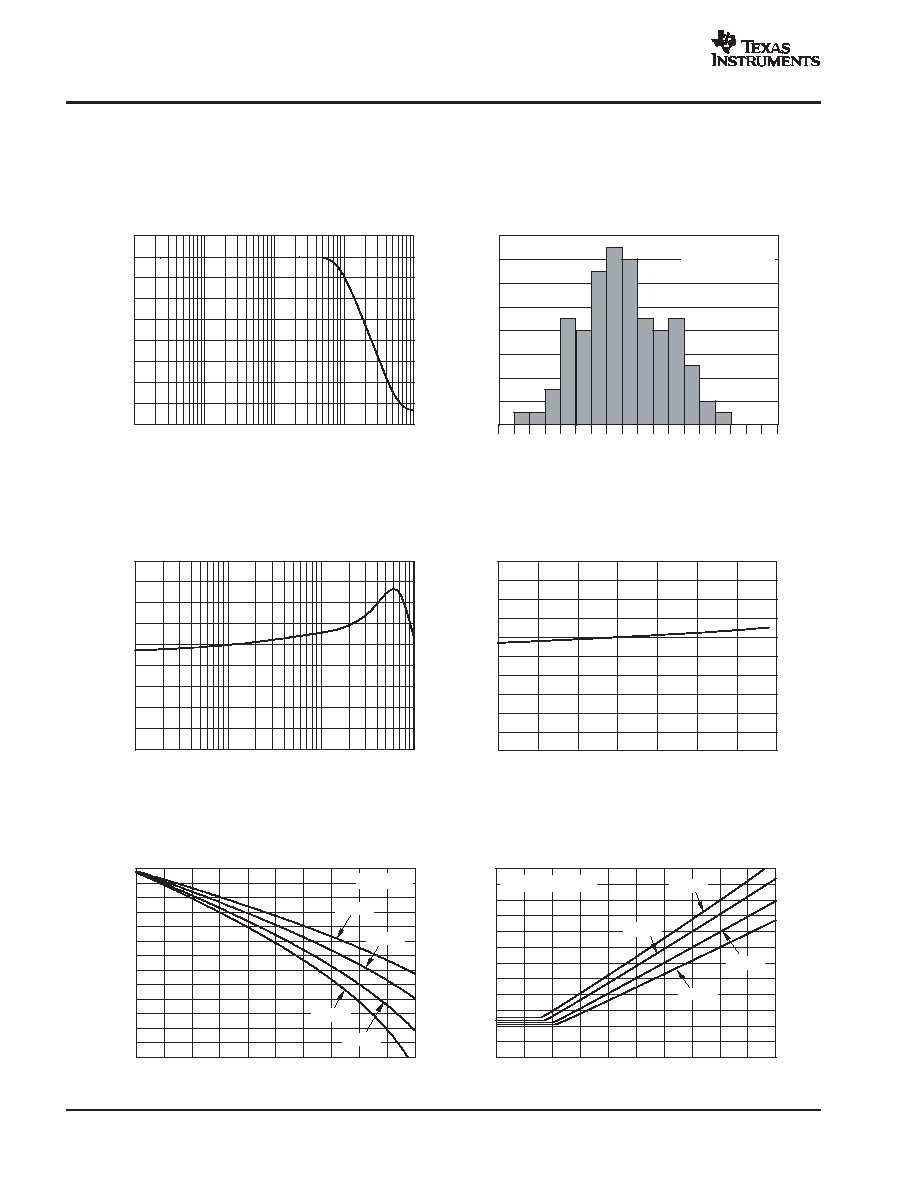
TYPICAL CHARACTERISTICS: V
S
= 3.3V
At TA = +25
�
C and RL = 150
, unless otherwise noted.
5
0
-
5
-
10
-
15
-
20
-
25
-
30
-
35
-
40
FREQUENCY RESPONSE
Frequency (Hz)
N
o
r
m
a
liz
e
d
G
a
in
(
d
B)
10k
100k
1M
10M
100M
Normalized Gain at 4.5MHz
Production Distribution
Normalized Gain at 4.5MHz (dB)
P
o
pu
l
a
t
i
on
-
0
.
325
-
0.3
-
0
.
275
-
0.25
-
0
.
225
-
0.2
-
0
.
175
-
0.15
-
0
.
125
-
0.1
-
0
.
075
-
0.05
-
0
.
025
0
0.02
5
0.
05
0.07
5
0.
1
-
0
.
125
Normalized:
"0" dB corresponds
to 6dB gain.
45
40
35
30
25
20
15
10
5
0
GROUP DELAY vs FREQUENCY
Frequency (Hz)
G
r
oup
D
e
l
a
y
(
n
s
)
10k
100k
1M
10M
2.0
1.8
1.6
1.4
1.2
1.0
0.8
0.6
0.4
0.2
0
GAIN ERROR
Temperature (
_
C)
Ga
i
n
E
rro
r
(
%
)
-
50
-
25
0
25
50
75
100
125
3.3
3.2
3.1
3.0
2.9
2.8
2.7
2.6
2.5
2.4
2.3
2.2
2.1
2.0
OUTPUT VOTLAGE SWING TO THE POSITIVE RAIL
vs OUTPUT CURRENT
Output Current (A)
O
u
t
p
u
t
Vo
lt
a
g
e
(
V)
0
0.01 0.02 0.03 0.04 0.05 0.06 0.07 0.08 0.09 0.1
V
S
= 3.3V
+85
_
C
-
40
_
C
+25
_
C
+125
_
C
0.30
0.25
0.20
0.15
0.10
0.05
0
OUTPUT VOLTAGE SWING TO THE NEGATIVE RAIL
vs OUTPUT CURRENT
Output Current (A)
O
u
t
p
u
t
Vo
lt
a
g
e
(
V)
0
0.01 0.02 0.03 0.04 0.05 0.06 0.07 0.08 0.09 0.1
V
S
= 3.3V, V
IN
= 0V
+125
_
C
-
40
_
C
+25
_
C
+85
_
C
OPA360
SB0S294C - DECEMBER 2003 - REVISED JULY 2004
www.ti.com
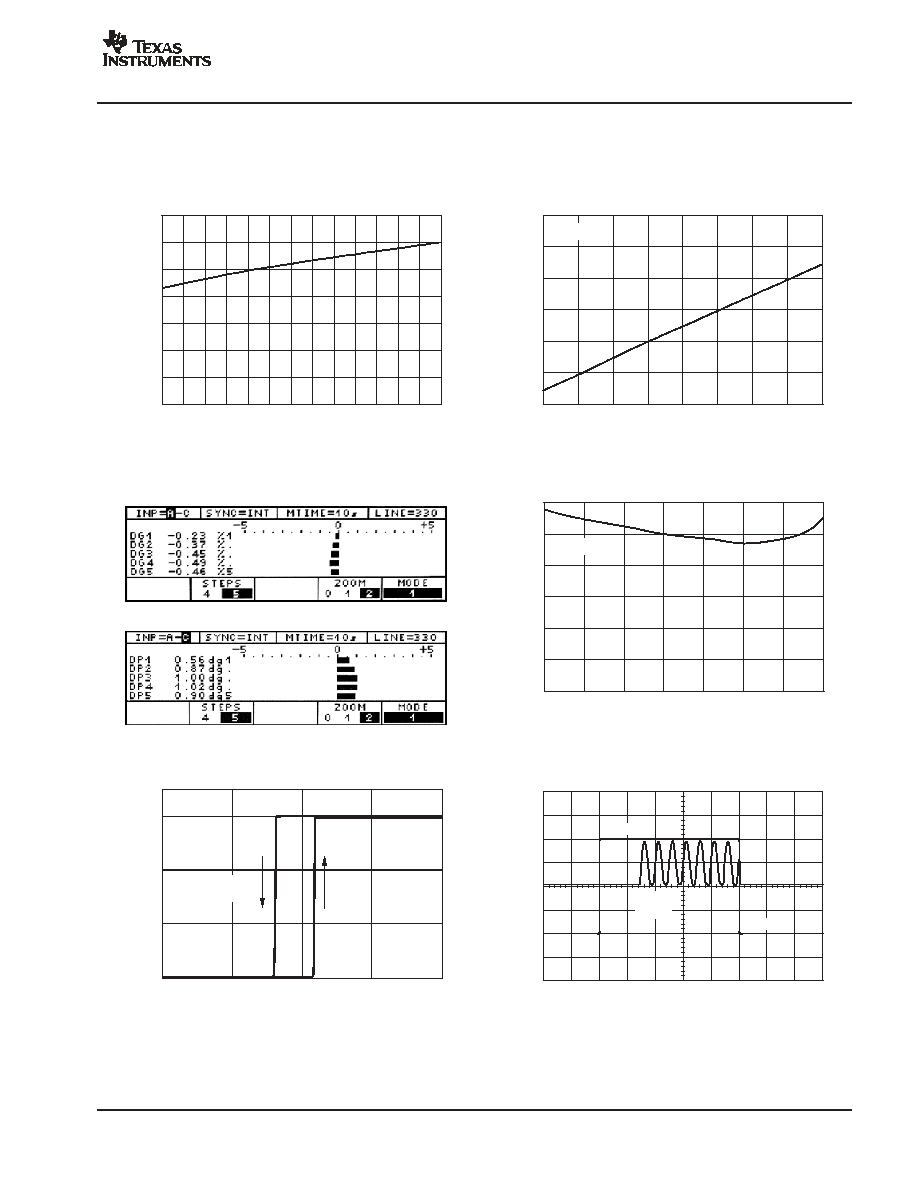
5
TYPICAL CHARACTERISTICS: V
S
= 3.3V (continued)
At TA = +25
�
C and RL = 150
, unless otherwise noted.
7
6
5
4
3
2
1
0
QUIESCENT CURRENT vs SUPPLY VOLTAGE
Supply Voltage (V)
Q
u
i
e
s
c
en
t
C
ur
r
e
nt
(
m
A
)
2.0 2.1 2.2 2.3 2.4 2.5 2.6 2.7 2.8 2.9 3.0 3.1 3.2 3.3
8.0
7.5
7.0
6.5
6.0
5.5
5.0
QUIESCENT CURRENT vs TEMPERATURE
Temperature (
_
C)
Q
u
i
e
s
c
ent
C
u
r
r
en
t
(
m
A
)
-
50
-
25
0
25
50
75
100
125
150
V
S
= 3.3V
DIFFERENTIAL GAIN
DIFFERENTIAL PHASE
3.0
2.5
2.0
1.5
1.0
0.5
0
SHUTDOWN CURRENT vs TEMPERATURE
Temperature (
_
C)
S
hutd
o
w
n
C
u
r
r
ent
(
�
A)
-
50
-
25
0
25
50
75
100
125
V
S
= 3.3V
6
4
2
0
SHUTDOWN TRIGGER LEVELS
Enable Pin Voltage (V)
Qu
i
e
sc
e
n
t
C
u
rre
n
t
(m
A
)
1.4
1.45
1.5
1.55
1.6
OPA360
Shutdown
OPA360
Active
LARGE-SIGNAL DISABLE/ENABLE RESPONSE
V
o
l
t
ag
e
(
5
0
0m
V
/
d
i
v
)
Time (1
�
s/div)
Enable
Disable
OPA360
Output
OPA360
SB0S294C - DECEMBER 2003 - REVISED JULY 2004
www.ti.com
6
APPLICATIONS INFORMATION
The OPA360 video amplifier has been optimized for
portable video applications:
D
Internal gain setting resistors (G = 2) reduce the
number of external components needed in the
video circuit.
D
A 2-pole filter is incorporated for DAC signal
reconstruction.
D
The sag correction function reduces the size of the
output coupling capacitors without compromising
performance.
D
OPA360 employs an internal level shift circuit that
avoids sync pulse clipping and allows DC-coupled
output.
D
A shutdown feature reduces quiescent current to
less than 5
�
A--crucial for portable applications
such as digital still cameras and camera phones.
The OPA360 interfaces to digital media processors
(DM320/270, DSC25). It has been optimized for the
requirements of digital still cameras and cell
phone/camera designs.
OPERATING VOLTAGE
The OPA360 is fully specified from 2.7V to 3.3V over a
temperature range of -40
�
C to +85
�
C. Parameters that
vary significantly with operating voltages or temperature
are shown in the Typical Characteristics.
Power-supply pins should be bypassed with 100nF
ceramic capacitors.
INPUT VOLTAGE
The input common-mode range of the OPA360 series
extends from GND to (V+) - 1.5V. Because of the internal
gain, the input voltage range necessary for an output in the
valid range will be limited.
INPUT OVERVOLTAGE PROTECTION
All OPA360 pins are static-protected with internal ESD
protection diodes connected to the supplies. These diodes
will provide input overdrive protection if the current is
externally limited to 10mA
ENABLE/SHUTDOWN
The OPA360 has a shutdown feature that disables the
output and reduces the quiescent current to less than 5
�
A.
This feature is especially useful for portable video
applications such as digital still cameras (DSC) and
camera phones, where the equipment is infrequently
connected to a TV or other video device.
The Enable logic input voltage is referenced to the
OPA360 GND pin. A logic level HIGH applied to the enable
pin enables the op amp. A valid logic HIGH is defined as
1.6V above GND. A valid logic LOW is defined as
0.8V
above GND. If the Enable pin is not connected, internal
pull-up circuitry will enable the amplifier. Enable pin
voltage levels are tested for a valid logic HIGH threshold
of 1.6V minimum and a valid logic LOW threshold of 0.8V
maximum.
INTERNAL 2-POLE FILTER
The OPA360 filter is a Sallen-Key topology with a 9MHz
cutoff frequency. This allows the video signals to pass
without any visible distortion, as shown in Figure 3 through
Figure 5. The video DACs embedded in TI's Digital Media
Processors over-sample at 27MHz. At this frequency, the
attenuation is typically 21dB, which effectively attenuates
the sampling aliases.
The filter characteristics vary somewhat with signal source
impedance. A source impedance greater than 500
can
degrade filter performance. With current-output video
DACs, a resistor to GND is often used to create a voltage
output which is then applied to the OPA360 input (see
Figure 1). TI's Digital Media Processors, such as the
DM270 or DM320, typically use a 200
resistor to GND to
convert the current output signal. This 200
source
impedance does not degrade video performance.
12pF
650
NOTE: (1) Optional.
325
1.4k
1.1k
528
845
V
O
R
SAG
OPA360
(1)
(
)
10pF
75
75
Television
Figure 1. Filter Structure of OPA360

OPA360
SB0S294C - DECEMBER 2003 - REVISED JULY 2004
www.ti.com
7
A capacitor placed in parallel with the resistor (Figure 1)
creates an additional filter pole that provides additional
stop-band attenuation. With a 200
source impedance, a
67pF ceramic capacitor provides approximately 28dB
attenuation at 27MHz without affecting the pass band.
VIDEO PERFORMANCE
Industry standard video test patterns include:
D
Multiburst--packets of different test frequencies to
check for basic frequency response.
D
Multipulse--pulses modulated at different
frequencies to test for comprehensive measurement
of amplitude and group delay errors across the video
baseband.
D
Chrominance-to-luminence (CCIR17) -- tests ampli-
tude, phase and some distortion
D
50Hz, 1/2 black-1/2 white screen test signal--tests
the worst case signal swing required by the amplifier.
Performance on these test signals are shown.
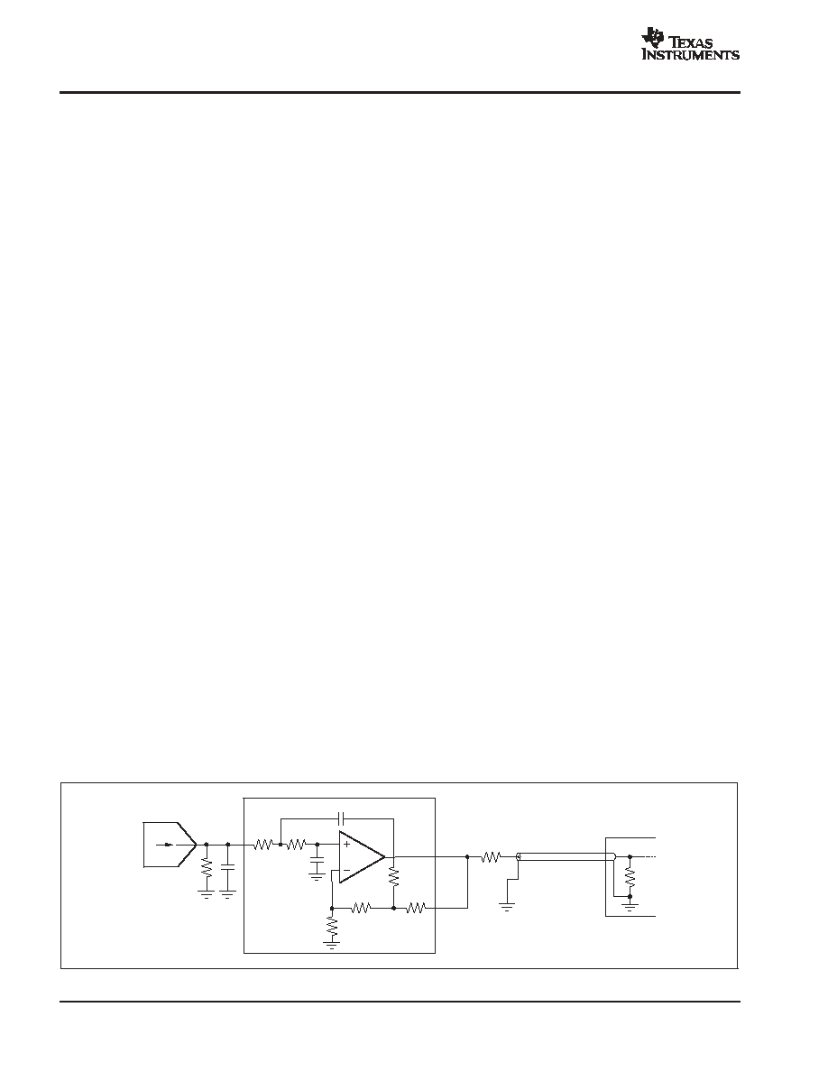
Figure 2 shows the test circuits for Figure 3 through
Figure 13 and Figure 16. (NOTE: 1 and 2 indicate
measurement points corresponding to the waveforms
labeled 1 and 2 in the figures.)
1
2
a. Test circuit for Figures 3-5.
2
d. Test circuit for Figures 7, 12, and 13.
1
c. Test circuits for Figures 10 and 11.
2
1
1
1
2
b. Test circuit for Figures 6, 8, and 16.
220
�
F
22
�
F
C
OUT
22
�
F
NOTE: 1 and 2 indicate measurement points corresponding to the waveforms labeled 1 and 2 in the figures.
SAG
47
�
F
22
�
F
Figure 2. Test Circuits Used for Figures 2-13
OPA360
SB0S294C - DECEMBER 2003 - REVISED JULY 2004
www.ti.com
8
FREQUENCY RESPONSE OF THE OPA360
Frequency response measurements evaluate the ability of
a video system to uniformly transfer signal components of
different frequencies without affecting their respective
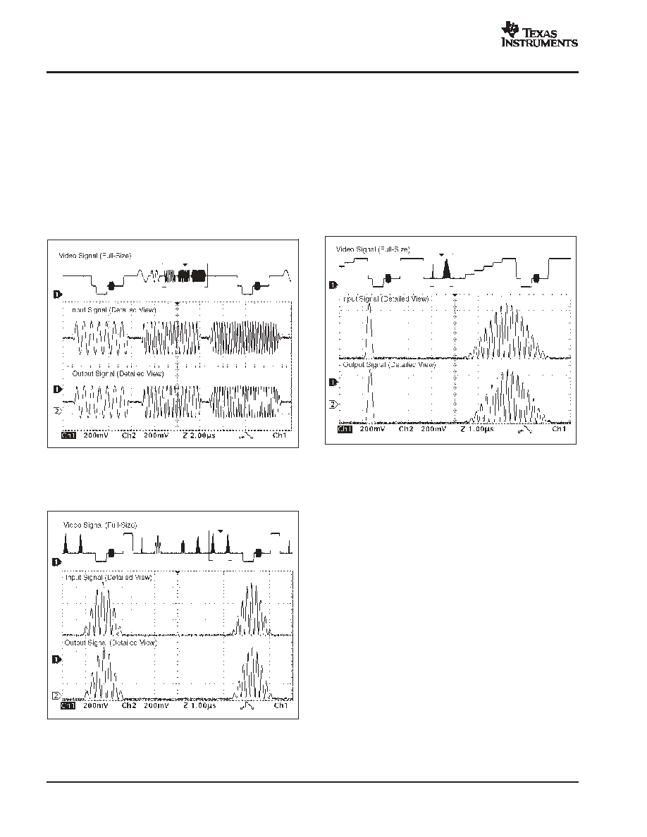
amplitudes. Figure 3 shows the multiburst test pattern;
Figure 4 shows the multipulse. The top waveforms in
these figures show the full test pattern. The middle and
bottom waveform are a more detailed view of the critical
portion of the full waveform. The middle waveform
represents the input signal from the video generator; the
bottom waveform is the OPA360 output to the line.
Figure 3. Multiburst (CCIR 18) Test Pattern (PAL)
Figure 4. Multipulse Test Pattern (PAL)
Chrominance-to-luminence gain inequality (or relative
chrominance level) is a change in the gain ratio of the
chrominance and luminence components of a video
signal, which are at different frequencies. A common test
pattern is the pulse in test pattern CCIR 17, shown in
Figure 5. As in Figure 3 and Figure 4 the top waveform
shows the full test pattern, the middle and bottom
waveform are a more detailed view of the critical portion of
the full waveform, with the middle waveform representing
the input signal from the video generator and the bottom
waveform being the OPA360 output to the line.
Figure 5. CCIR 17 Test Pattern (PAL)
Gain errors most commonly appear as attenuation or
peaking of the chrominance information. This shows up in
the picture as incorrect color saturation. Delay distortion
will cause color smearing or bleeding, particularly at the
edges of objects in the picture. It may also cause poor
reproduction of sharp luminence transitions.
All waveforms in Figure 3 through Figure 5 were taken
using the sag correction feature of OPA360. Figure 3
through Figure 5 show that the OPA360 causes no visible
distortion or change in gain throughout the entire video
frequency range.
INTERNAL LEVEL SHIFT
Many common video DACs embedded in digital media
processors like TI's TMS320DM270 and the new
OMAP2420 processors operate on a single supply (no
negative supply). Typically, the lowest point of the sync
pulse output by these Video DACs corresponds to 0V. With
a 0V input, the output of common single-supply op amps
saturates at a voltage > 0V. This effect would clip the tip of
the sync pulse and therefore degrade the video signal
integity. The OPA360 employs an internal level shift circuit
to avoid clipping. The input signal is typically shifted by
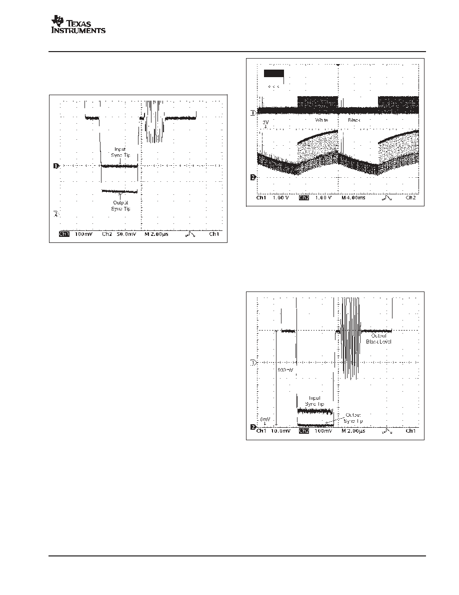
OPA360
SB0S294C - DECEMBER 2003 - REVISED JULY 2004
www.ti.com
9
approximately 60mV. This is well within the linear output
voltage range of the OPA360 with a standard 150
video
load. Figure 6 shows the function of the level shifter.
Figure 6. Internal Level Shifter, Shifts Input
Signal by Approximately 60mV to Prevent Sync
Tip Clipping
The level shift function is particularly useful when the
output of the OPA360 is DC-coupled to the video load.
However, it is also helpful when sag correction is
employed. The offset helps to shift the video signal closer
to the positive rail, so that with even a small 33
�
F coupling
capacitor, the output is well outside the saturation limits of
the OPA360. Figure 7 shows the output swing of the
OPA360, operated on 3.0V supplies, with a 22
�
F sag
correction capacitor and a 33
�
F output coupling capacitor.
The test signal is a 50Hz signal constructed to generate a
1/2 black, 1/2 white screen. This video pattern is one of the
most difficult patterns to display because it is the worst
case signal regarding signal swing. A worst case signal
such as this is highly unlikely in normal operation. Any
other signal has a lower swing range. Note in Figure 7 that
neither the white nor the black portion of the video signal
is clipped.
Figure 7. Output Swing with 33
m
F on 3V Supply
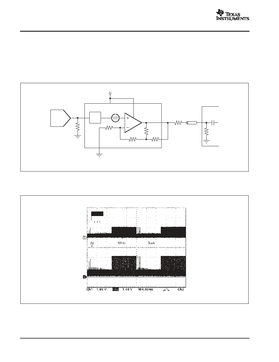
OUTPUT SWING TO GND (SYNC PULSE)
Figure 8 shows the true output swing capability of the
OPA360 by taking the tip of the input sync pulse to a
slightly negative voltage. Even when the output sync tip is
at 8mV, the output shows no clipping of the sync pulse.
Figure 8. Input Sync Tip at -30mV (Output Shows
No Sign of Clipping)
OPA360
SB0S294C - DECEMBER 2003 - REVISED JULY 2004
www.ti.com
10
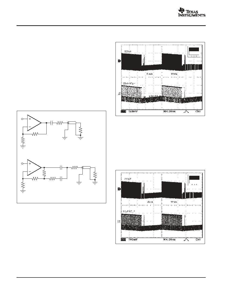
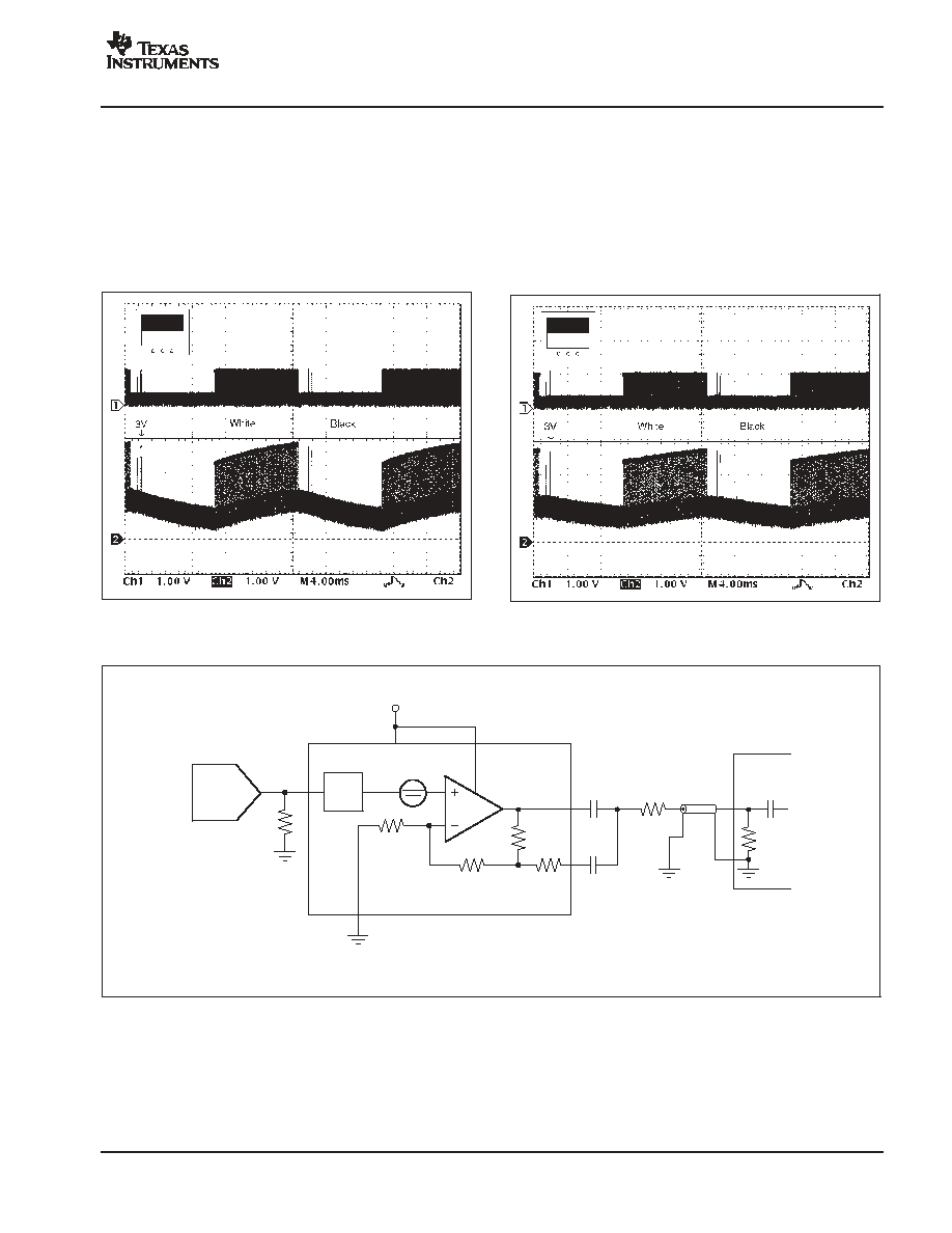
SAG CORRECTION
Sag correction provides excellent video performance with
two small output coupling capacitors. It eliminates the
traditional, large 220
�
F output capacitor. The traditional
220
�
F circuit (Figure 9a) creates a single low frequency
pole (-3dB frequency) at 5Hz. If this capacitor is made
much smaller, excessive phase shift in the critical 50 to
100Hz range produces field tilt which can interfere with
proper recovery of synchronization signals in the television
receiver.
The OPA360 sag correction circuit (Figure 9b, see also
Figure 14) creates an amplitude response peak in the
20Hz region. This small amount of peaking (a few tenths
of a dB) provides compensation of the phase response in
the critical 50Hz to 100Hz range, greatly reducing field tilt.
Note that two significantly smaller and lower cost
capacitors are required.
220
�
F 75
75
a) Traditional Video Circuit
47
�
F
75
22
�
F
75
b) OPA360 with Sag Connection
Figure 9. Traditional Video Circuit vs OPA360
with Sag Correction
To achieve good performance, a 22
�
F sag correction and
47
�
F coupling capacitor can be used. Figure 10 and
Figure 11 show comparisons for a standard video circuit
with a 220
�
F coupling capacitor and the OPA360 with sag
correction.
Figure 10 shows that the 22
�
F/47
�
F combination leads to
only a slightly greater tilt in the 50Hz, 1/2 black - 1/2 white
video signal. No degradation in video quality is observed.
Figure 10. Standard Video Circuit with 220
m
F
Capacitor (top trace) vs OPA360 with 22
m
F and
47
m
F Capacitors
A field tilt equivalent to that achieved using the standard
220
�
F coupling capacitor can be achieved with a
22
�
F/67
�
F combination - see Figure 11. These capacitor
values are optimized--sag correction capacitors larger
than 22
�
F do not provide significant improvement. Smaller
sag correction capacitors will lead to higher tilt.
Figure 11. 220
m
F Standard Video Circuit (top
trace) vs OPA360 with 22
m
F/67
m
F
OPA360
SB0S294C - DECEMBER 2003 - REVISED JULY 2004
www.ti.com
11
SUPPLY VOLTAGE vs COUPLING CAPACITOR
The output voltage swing is a function of the coupling
capacitor value. The value of the sag correction capacitor
has only a minor influence. The smaller the coupling
capacitor, the greater the output swing. Therefore, to
accommodate the large signal swing with very small
coupling capacitors (22
�
F and 33
�
F), a higher supply
voltage might be needed.
Figure 12. Output Swing with 47
m
F on 3V Supply
As seen in Figure 7, the output swing with a 33
�
F coupling
capacitor is already very close to the saturation limit on a
3V supply. Over time and temperature, a capacitor might
change its value slightly, which in turn could force the
output into saturation. Using the 50Hz, 1/2 black
1/2
white screen test signal as a worst-case analysis,
Figure 12 and Figure 13 demonstrate that a 3V supply
could be used with a coupling capacitor as low as 47
�
F.
Figure 13. Output Swing with 67
m
F on 3V Supply
C
OUT
47
�
F
R
OUT
75
GND
75
+
+
OUT
Enable
2-Pole
Filter
(1)
SAG
C
SAG
22
�
F
AC Gain = 2
DC Gain = 2.8
Television
or VCR
OPA360
Video
DAC
NOTE: (1) Optional 200
for use with TI's Digital Media Processors.
Level
Shifter
V+
V+ = 2.7V to 3.3V
Figure 14. DC-Coupled Input/AC-Coupled Output
OPA360
SB0S294C - DECEMBER 2003 - REVISED JULY 2004
www.ti.com
12
DC COUPLED OUTPUT
Due to the internal level shift, the OPA360 can also be DC-
coupled to a video load. As shown in Figure 15, this
eliminates the need for AC-coupling capacitors at the
output. This is especially important in portable video
applications where board space is restricted.
The DC-coupled output configuration also shows the best
video performance. As seen in Figure 16, there is no line
or field tilt--allowing use of the lowest power supply. In this
mode, the OPA360 will safely operate down to 2.5V with
no clipping of the signal.
The disadvantage with DC-coupled output is that it uses
somewhat higher supply current.
R
OUT
75
GND
Level
Shifter
OUT
Enable
6dB
2-Pole
Filter
V+
V+ = 2.7V to 3.3V
SAG
OPA360
(1)
Video
DAC
NOTE: (1) Optional 200
for use with TI's Digital Media Processors.
75
Television
or VCR
Figure 15. DC-Coupled Input/DC-Coupled Output
Figure 16. DC-Coupled Output

PACKAGING INFORMATION
ORDERABLE DEVICE
STATUS(1)
PACKAGE TYPE
PACKAGE DRAWING
PINS
PACKAGE QTY
OPA360AIDCKR
ACTIVE
SOP
DCK
6
3000
OPA360AIDCKT
ACTIVE
SOP
DCK
6
250
(1) The marketing status values are defined as follows:
ACTIVE: Product device recommended for new designs.
LIFEBUY: TI has announced that the device will be discontinued, and a lifetime-buy period is in effect.
NRND: Not recommended for new designs. Device is in production to support existing customers, but TI does not recommend using this part in
a new design.
PREVIEW: Device has been announced but is not in production. Samples may or may not be available.
OBSOLETE: TI has discontinued the production of the device.
PACKAGE OPTION ADDENDUM
www.ti.com
20-Jul-2004

MECHANICAL DATA
MPDS114 � FEBRUARY 2002
POST OFFICE BOX 655303
�
DALLAS, TEXAS 75265
DCK (R-PDSO-G6)
PLASTIC SMALL-OUTLINE PACKAGE
0,15
Gage Plane
0,10
M
0,10
0,65
0
�
�8
�
0,46
0,26
0,13 NOM
4093553-3/D 01/02
0,15
0,30
1,40
1,10
2,40
1,80
4
6
2,15
1,85
1
3
1,10
0,80
0,10
0,00
Seating Plane
NOTES: A. All linear dimensions are in millimeters.
B. This drawing is subject to change without notice.
C. Body dimensions do not include mold flash or protrusion.
D. Falls within JEDEC MO-203

IMPORTANT NOTICE
Texas Instruments Incorporated and its subsidiaries (TI) reserve the right to make corrections, modifications,
enhancements, improvements, and other changes to its products and services at any time and to discontinue
any product or service without notice. Customers should obtain the latest relevant information before placing
orders and should verify that such information is current and complete. All products are sold subject to TI's terms
and conditions of sale supplied at the time of order acknowledgment.
TI warrants performance of its hardware products to the specifications applicable at the time of sale in
accordance with TI's standard warranty. Testing and other quality control techniques are used to the extent TI
deems necessary to support this warranty. Except where mandated by government requirements, testing of all
parameters of each product is not necessarily performed.
TI assumes no liability for applications assistance or customer product design. Customers are responsible for
their products and applications using TI components. To minimize the risks associated with customer products
and applications, customers should provide adequate design and operating safeguards.
TI does not warrant or represent that any license, either express or implied, is granted under any TI patent right,
copyright, mask work right, or other TI intellectual property right relating to any combination, machine, or process
in which TI products or services are used. Information published by TI regarding third-party products or services
does not constitute a license from TI to use such products or services or a warranty or endorsement thereof.
Use of such information may require a license from a third party under the patents or other intellectual property
of the third party, or a license from TI under the patents or other intellectual property of TI.
Reproduction of information in TI data books or data sheets is permissible only if reproduction is without
alteration and is accompanied by all associated warranties, conditions, limitations, and notices. Reproduction
of this information with alteration is an unfair and deceptive business practice. TI is not responsible or liable for
such altered documentation.
Resale of TI products or services with statements different from or beyond the parameters stated by TI for that
product or service voids all express and any implied warranties for the associated TI product or service and
is an unfair and deceptive business practice. TI is not responsible or liable for any such statements.
Following are URLs where you can obtain information on other Texas Instruments products and application
solutions:
Products
Applications
Amplifiers
amplifier.ti.com
Audio
www.ti.com/audio
Data Converters
dataconverter.ti.com
Automotive
www.ti.com/automotive
DSP
dsp.ti.com
Broadband
www.ti.com/broadband
Interface
interface.ti.com
Digital Control
www.ti.com/digitalcontrol
Logic
logic.ti.com
Military
www.ti.com/military
Power Mgmt
power.ti.com
Optical Networking
www.ti.com/opticalnetwork
Microcontrollers
microcontroller.ti.com
Security
www.ti.com/security
Telephony
www.ti.com/telephony
Video & Imaging
www.ti.com/video
Wireless
www.ti.com/wireless
Mailing Address:
Texas Instruments
Post Office Box 655303 Dallas, Texas 75265
Copyright
2004, Texas Instruments Incorporated