 | –≠–ª–µ–∫—Ç—Ä–æ–Ω–Ω—ã–π –∫–æ–º–ø–æ–Ω–µ–Ω—Ç: OPA4342EA | –°–∫–∞—á–∞—Ç—å:  PDF PDF  ZIP ZIP |
Low Cost, Low Power, Rail-to-Rail
OPERATIONAL AMPLIFIERS
Micro
Amplifier
TM
Series
© 1999 Burr-Brown Corporation
PDS-1485B
Printed in U.S.A. June, 2000
Æ
FEATURES
q
LOW QUIESCENT CURRENT: 150
µ
A typ
q
RAIL-TO-RAIL INPUT
q
RAIL-TO-RAIL OUTPUT (within 1mV)
q
SINGLE SUPPLY CAPABILITY
q
LOW COST
q
Micro
SIZE PACKAGE OPTIONS:
SOT23-5
MSOP-8
TSSOP-14
q
BANDWIDTH: 1MHz
q
SLEW RATE: 1V/
µ
s
q
THD + NOISE: 0.006%
APPLICATIONS
q
COMMUNICATIONS
q
PCMCIA CARDS
q
DATA ACQUISITION
q
PROCESS CONTROL
q
AUDIO PROCESSING
q
ACTIVE FILTERS
q
TEST EQUIPMENT
q
CONSUMER ELECTRONICS
DESCRIPTION
The OPA342 series rail-to-rail CMOS operational
amplifiers are designed for low cost, low power,
miniature applications. They are optimized to operate
on a single supply as low as 2.5V with an input
common-mode voltage range that extends 300mV
beyond the supplies.
Rail-to-rail input/output and high-speed operation make
them ideal for driving sampling Analog-to-Digital Con-
verters (ADC). They are also well suited for general
purpose and audio applicaitons and providing I/V con-
version at the output of Digital-to-Analog Converters
(DAC). Single, dual and quad versions have identical
specs for design flexibility.
The OPA342 series offers excellent dynamic response
with a quiescent current of only 250
µ
A max. Dual and
quad designs feature completely independent circuitry
for lowest crosstalk and freedom from interaction.
OPA342
OPA2342
OPA4342
International Airport Industrial Park ∑ Mailing Address: PO Box 11400, Tucson, AZ 85734 ∑ Street Address: 6730 S. Tucson Blvd., Tucson, AZ 85706 ∑ Tel: (520) 746-1111
Twx: 910-952-1111 ∑ Internet: http://www.burr-brown.com/ ∑ Cable: BBRCORP ∑ Telex: 066-6491 ∑ FAX: (520) 889-1510 ∑ Immediate Product Info: (800) 548-6132
For most current data sheet and other product
information, visit www.burr-brown.com
Æ
OPA342
OPA342
OPA2342
OPA4342
OPA4342
SINGLE
DUAL
QUAD
PACKAGE
OPA342
OPA2342
OPA4342
SOT23-5
MSOP-8
SO-8
TSSOP-14
SO-14
DIP-14
SPICE MODEL available at www.burr-brown.com.
2
Æ
OPA342, 2342, 4342
SPECIFICATIONS: V
S
= 2.7V to 5.5V
At T
A
= +25
∞
C, R
L
= 10k
connected to V
S
/ 2 and V
OUT
= V
S
/ 2, unless otherwise noted.
Boldface limits apply over the temperature range, T
A
= ≠40
∞
C to +85
∞
C.
OPA342NA, UA
OPA2342EA, UA
OPA4342EA, UA, PA
PARAMETER
CONDITION
MIN
TYP
MAX
UNITS
OFFSET VOLTAGE
Input Offset Voltage
V
OS
V
CM
= V
S
/ 2
±
1
±
6
mV
T
A
= ≠40
∞
C to +85
∞
C
±
1
±
6
mV
vs Temperature
dV
OS
/dT
±
3
µ
V/
∞
C
vs Power Supply
PSRR
V
S
= 2.7V to 5.5V, V
CM
< (V+) -1.8V
30
200
µ
V/V
T
A
= ≠40
∞
C to +85
∞
C
V
S
= 2.7V to 5.5V, V
CM
< (V+) -1.8V
250
µ
V/V
Channel Separation, dc
0.2
µ
V/V
f = 1kHz
132
dB
INPUT BIAS CURRENT
Input Bias Current
I
B
±
0.2
±
10
pA
T
A
= ≠40
∞
C to +85
∞
C
See Typical Curve
pA
Input Offset Current
I
OS
±
0.2
±
10
pA
NOISE
Input Voltage Noise, f = 0.1Hz to 50kHz
8
µ
Vrms
Input Voltage Noise Density, f = 1kHz
e
n
30
nV/
Hz
Current Noise Density, f = 1kHz
i
n
0.5
fA/
Hz
INPUT VOLTAGE RANGE
Common-Mode Voltage Range
V
CM
≠0.3
(V+) + 0.3
V
Common-Mode Rejection Ratio
CMRR
V
S
= +5.5V, ≠0.3V
< V
CM
< (V+) - 1.8
76
88
dB
T
A
= ≠40
∞
C to +85
∞
C
V
S
= +5.5V, ≠0.3V
< V
CM
< (V+) - 1.8
74
dB
Common-Mode Rejection Ratio
CMRR
V
S
= +5.5V, ≠0.3V
< V
CM
< 5.8V
66
78
dB
T
A
= ≠40
∞
C to +85
∞
C
V
S
= +5.5V, ≠0.3V
< V
CM
< 5.8V
64
dB
Common-Mode Rejection Ratio
CMRR
V
S
= +2.7V, ≠0.3V
< V
CM
< 3V
62
74
dB
T
A
= ≠40
∞
C to +85
∞
C
V
S
= +2.7V, ≠0.3V
< V
CM
< 3V
60
dB
INPUT IMPEDANCE
Differential
10
13
|| 3
|| pF
Common-Mode
10
13
|| 6
|| pF
OPEN-LOOP GAIN
Open-Loop Voltage Gain
A
OL
R
L
= 100k
, 10mV < V
O
< (V+) ≠ 10mV
104
124
dB
T
A
= ≠40
∞
C to +85
∞
C
R
L
= 100k
, 10mV < V
O
< (V+) ≠ 10mV
100
dB
R
L
= 5k
, 400mV < V
O
< (V+) ≠ 400mV
96
114
dB
T
A
= ≠40
∞
C to +85
∞
C
R
L
= 5k
, 400mV < V
O
< (V+) ≠ 400mV
90
dB
FREQUENCY RESPONSE
C
L
= 100pF
Gain-Bandwidth Product
GBW
G = 1
1
MHz
Slew Rate
SR
1
V/
µ
s
Settling Time, 0.1%
V
S
= 5.5V, 2V Step
5
µ
s
0.01%
V
S
= 5.5V, 2V Step
8
µ
s
Overload Recovery Time
V
IN
∑ G = V
S
2.5
µ
s
Total Harmonic Distortion + Noise, f = 1kHz THD+N
V
S
= 5.5V, V
O
= 3Vp-p
(1)
, G = 1
0.006
%
OUTPUT
Voltage Output Swing from Rail
(2)
R
L
= 100k
, A
OL
96dB
1
mV
R
L
= 100k
,
A
OL
104dB
3
10
mV
T
A
= ≠40
∞
C to +85
∞
C
R
L
= 100k
,
A
OL
100dB
10
mV
R
L
= 5k
, A
OL
96dB
20
400
mV
T
A
= ≠40
∞
C to +85
∞
C
R
L
= 5k
,
A
OL
90dB
400
mV
Short-Circuit Current
I
SC
Per Channel
±
15
mA
Capacitive Load Drive
C
LOAD
See Typical Curve
POWER SUPPLY
Specified Voltage Range
V
S
2.7
5.5
V
Operating Voltage Range
2.5 to 5.5
V
Quiescent Current (per amplifier)
I
Q
I
O
= 0A
150
250
µ
A
T
A
= ≠40
∞
C to +85
∞
C
300
µ
A
TEMPERATURE RANGE
Specified Range
≠40
+85
∞
C
Operating Range
≠55
+125
∞
C
Storage Range
≠65
+150
∞
C
Thermal Resistance
JA
SOT23-5 Surface Mount
200
∞
C/W
MSOP-8 Surface Mount
150
∞
C/W
SO-8 Surface Mount
150
∞
C/W
TSSOP-14 Surface Mount
100
∞
C/W
SO-14 Surface Mount
100
∞
C/W
DIP-14
100
∞
C/W
NOTE: (1) V
OUT
= 0.25V to 3.25V. (2) Output voltage swings are measured between the output and power-supply rails.

3
Æ
OPA342, 2342, 4342
PACKAGE
SPECIFIED
DRAWING
TEMPERATURE
PACKAGE
ORDERING
TRANSPORT
PRODUCT
PACKAGE
NUMBER
RANGE
MARKING
NUMBER
(1)
MEDIA
OPA342NA
SOT23-5
331
≠40
∞
C to +85
∞
C
B42
OPA342NA /250
Tape and Reel
"
"
"
"
"
OPA342NA /3K
Tape and Reel
OPA342UA
SO-8
182
≠40
∞
C to +85
∞
C
OPA342UA
OPA342UA
Rails
"
"
"
"
"
OPA342UA /2K5
Tape and Reel
OPA2342EA
MSOP-8
337
≠40
∞
C to +85
∞
C
C42
OPA2342EA /250
Tape and Reel
"
"
"
"
"
OPA2342EA /2K5
Tape and Reel
OPA2342UA
SO-8
182
≠40
∞
C to +85
∞
C
OPA2342UA
OPA2342UA
Rails
"
"
"
"
"
OPA2342UA /2K5
Tape and Reel
OPA4342EA
TSSOP-14
357
≠40
∞
C to +85
∞
C
OPA4342EA
OPA4342EA /250
Tape and Reel
"
"
"
"
"
OPA4342EA /2K5
Tape and Reel
OPA4342UA
SO-14
235
≠40
∞
C to +85
∞
C
OPA4342UA
OPA4342UA
Rails
"
"
"
"
"
OPA4342UA /2K5
Tape and Reel
OPA4342PA
DIP-14
010
≠40
∞
C to +85
∞
C
OPA4342PA
OPA4342PA
Rails
NOTE: (1) Models with a slash (/) are available only in Tape and Reel in the quantities indicated (e.g., /3K indicates 3000 devices per reel). Ordering 3000 pieces
of "OPA342NA/3K" will get a single 3000-piece Tape and Reel.
PACKAGE/ORDERING INFORMATION
Supply Voltage, V+ to V- ................................................................... 7.5V
Signal Input Terminals, Voltage
(2)
..................... (V≠) ≠0.5V to (V+) +0.5V
Current
(2)
.................................................... 10mA
Output Short-Circuit
(3)
.............................................................. Continuous
Operating Temperature .................................................. ≠55
∞
C to +125
∞
C
Storage Temperature ..................................................... ≠65
∞
C to +150
∞
C
Junction Temperature ...................................................................... 150
∞
C
Lead Temperature (soldering, 10s) ................................................. 300
∞
C
ESD Tolerance (Human Body Model) ............................................ 4000V
NOTES: (1) Stresses above these ratings may cause permanent damage.
Exposure to absolute maximum conditions for extended periods may
degrade device reliability. These are stress ratings only. Functional opera-
tion of the device at these conditions, or beyond the specified operating
conditions, is not implied. (2) Input terminals are diode-clamped to the power
supply rails. Input signals that can swing more than 0.5V beyond the supply
rails should be current-limited to 10mA or less. (3) Short-circuit to ground,
one amplifier per package.
ABSOLUTE MAXIMUM RATINGS
(1)
ELECTROSTATIC
DISCHARGE SENSITIVITY
This integrated circuit can be damaged by ESD. Burr-Brown
recommends that all integrated circuits be handled with
appropriate precautions. Failure to observe proper handling
and installation procedures can cause damage.
ESD damage can range from subtle performance degrada-
tion to complete device failure. Precision integrated circuits
may be more susceptible to damage because very small
parametric changes could cause the device not to meet its
published specifications.
4
Æ
OPA342, 2342, 4342
TYPICAL PERFORMANCE CURVES
At T
A
= +25
∞
C, V
S
= +5V, and R
L
= 10k
connected to V
S
/2, unless otherwise noted.
POWER SUPPLY AND COMMON-MODE
REJECTION RATIO vs FREQUENCY
10
Rejection Ratio (dB)
Frequency (Hz)
100
1k
10k
100k
100
80
60
40
20
10
+PSRR
CMRR
≠PSRR
CHANNEL SEPARATION vs FREQUENCY
100
Channel Separation (dB)
Frequency (Hz)
1k
10k
100k
1M
140
120
100
80
60
Dual and quad devices.
G = 1, all channels.
Quad measured channel
A to D or B to C--other
combinations yield improved
rejection.
VOLTAGE AND CURRENT NOISE
SPECTRAL DENSITY vs FREQUENCY
1
Voltage Noise (nV/
Hz)
Frequency (Hz)
10
100
1k
10k
100k
1M
10M
10000
1000
100
10
Current Noise (fA/
Hz)
100
10
1
0.1
V
N
I
N
TOTAL HARMONIC DISTORTION + NOISE
vs FREQUENCY
20
THD+N (%)
Frequency (Hz)
100
1k
10k
20k
1
0.1
0.010
0.001
OPEN-LOOP GAIN/PHASE vs FREQUENCY
0.1
1
Gain (dB)
0
30
60
90
120
150
180
Phase (
∞
)
Frequency (Hz)
10
100
1k
10k
100k
1M
10M
120
100
80
60
40
20
0
Gain
Phase
MAXIMUM OUTPUT VOLTAGE vs FREQUENCY
10k
Maximum Output Voltage (Vp-p)
Frequency (Hz)
100k
1M
6
5
4
3
2
1
0
V
S
= +2.7V
V
S
= +5.5V
V
S
= +5V
5
Æ
OPA342, 2342, 4342
TYPICAL PERFORMANCE CURVES
(Cont.)
At T
A
= +25
∞
C, V
S
= +5V, and R
L
= 10k
connected to V
S
/2, unless otherwise noted.
OPEN-LOOP GAIN, COMMON-MODE REJECTION RATIO,
AND POWER SUPPLY REJECTION vs TEMPERATURE
A
OL
≠75
A
OL
, CMRR, PSRR (dB)
Temperature (
∞
C)
≠25
0
25
≠50
50
125
75
100
150
140
120
100
80
60
40
20
0
CMRR
PSRR
INPUT BIAS CURRENT vs TEMPERATURE
≠75
Input Bias Current (pA)
Temperature (
∞
C)
≠25
0
25
≠50
100
50
75
125
10000
1000
100
10
1
0.1
QUIESCENT CURRENT AND
SHORT-CIRCUIT CURRENT vs TEMPERATURE
≠75
≠50
0
Quiescent Current (
µ
A)
Temperature (
∞
C)
25
50
100
I
Q
+I
SC
≠I
SC
75
≠25
125
200
175
150
135
100
75
50
25
0
Short-Circuit Current (mA)
40
35
30
25
20
15
10
5
0
SLEW RATE vs TEMPERATURE
≠75
Slew Rate (V/
µ
s)
Temperature (
∞
C)
25
0
≠SR
+SR
75
50
≠25
≠50
100
125
1.2
1
0.8
0.6
0.4
0.2
0
INPUT BIAS CURRENT
vs COMMON-MODE VOLTAGE
≠1
Input Bias Current (pA)
Common-Mode Voltage (V)
0
1
2
4
3
5
6
6
4
2
0
≠2
≠4
≠6
V+
Supply
V≠
Supply
Input voltage
≠0.3V
can cause op amp output
to lock up. See text.
QUIESCENT CURRENT AND
SHORT-CIRCUIT CURRENT vs SUPPLY VOLTAGE
Quiescent Current (
µ
A)
Supply Voltage (V)
2
3
4
5
6
+I
SC
≠I
SC
I
Q
160
155
150
145
140
Short-Circuit Current (mA)
20
15
10
5
0
6
Æ
OPA342, 2342, 4342
TYPICAL PERFORMANCE CURVES
(Cont.)
At T
A
= +25
∞
C, V
S
= +5V, and R
L
= 10k
connected to V
S
/2, unless otherwise noted.
OUTPUT VOLTAGE SWING vs OUTPUT CURRENT
0
Output Voltage (V)
Output Current (mA)
5
10
15
20
V+
(V+) ≠ 1
(V+) ≠ 2
2
1
0
85
∞
C
25
∞
C
≠40
∞
C
85
∞
C
25
∞
C
≠40
∞
C
OPEN-LOOP GAIN vs OUTPUT VOLTAGE SWING
120
110
100
90
80
Open-Loop Gain (dB)
Output Voltage Swing from Rail (mV)
120
100
80
60
40
20
0
R
L
= 5k
R
L
= 100k
OFFSET VOLTAGE
PRODUCTION DISTRIBUTION
Percent of Amplifiers (%)
Offset Voltage (mV)
≠6
≠5.4
≠4.8
≠4.2
≠3.6
≠3
≠2.4
≠1.8
≠1.2
≠0.6
0
0.6
1.2
1.8
2.4
3
3.6
4.2
4.8
5.4
6
24
20
16
12
8
4
0
Typical production
distribution of
packaged units.
OFFSET VOLTAGE DRIFT
PRODUCTION DISTRIBUTION
Percent of Amplifiers (%)
Offset Voltage Drift (
µ
V/
∞
C)
18
16
14
12
10
8
6
4
2
0
Typical production
distribution of
packaged units.
≠10
≠9
≠8
≠7
≠6
≠5
≠4
≠3
≠2
≠1
0
1
2
3
4
5
6
7
8
9
10
Quiescent Current (
µ
A)
QUIESCENT CURRENT
PRODUCTION DISTRIBUTION
24
20
16
12
8
4
0
Percent of Amplifiers (%)
<0
<25
<50
<75
<100
<125
<150
<175
<200
<225
<250
SETTLING TIME vs CLOSED-LOOP GAIN
1
Settling Time (
µ
s)
Closed-Loop Gain (V/V)
10
100
0.01%
0.1%
1000
400
350
300
250
200
150
100
50
0

7
Æ
OPA342, 2342, 4342
TYPICAL PERFORMANCE CURVES
(Cont.)
At T
A
= +25
∞
C, V
S
= +5V, and R
L
= 10k
connected to V
S
/2, unless otherwise noted.
SMALL-SIGNAL OVERSHOOT vs LOAD CAPACITANCE
1
Small-Signal Overshoot (%)
Load Capacitance (pF)
10
100
1k
10k
G = ≠1
G = ≠5
50
45
40
35
30
25
20
15
10
5
0
G = +5
G = +1
5
µ
s/div
LARGE-SIGNAL STEP RESPONSE
G = +1, R
L
= 10k
, C
L
= 100pF
1V/div
5
µ
s/div
SMALL-SIGNAL STEP RESPONSE
G = +1, R
L
= 10k
, C
L
= 100pF
20mV/div
8
Æ
OPA342, 2342, 4342
APPLICATIONS INFORMATION
OPA342 series op amps are unity gain stable and can operate
on a single supply, making them highly versatile and easy to
use.
Rail-to-rail input and output swing significantly increases
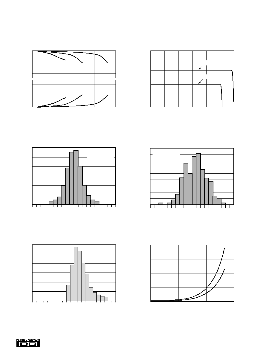
dynamic range, especially in low supply applications. Figure
1 shows the input and output waveforms for the OPA342 in
unity-gain configuration. Operation is from V
S
= +5V with
a 10k
load connected to V
S
/2. The input is a 5Vp-p
sinusoid. Output voltage is approximately 4.997Vp-p.
Power supply pins should be by passed with 0.01pF ceramic
capacitors.
OPERATING VOLTAGE
OPA342 series op amps are fully specified and guaranteed
from +2.7V to +5.5V. In addition, many specifications apply
from ≠40∫C to +85∫C. Parameters that vary significantly
with operating voltages or temperature are shown in the
Typical Performance Curves.
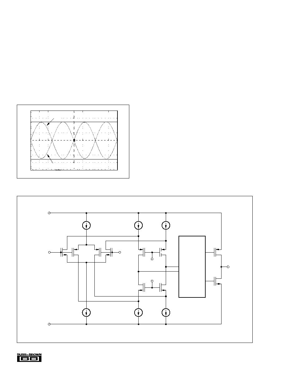
RAIL-TO-RAIL INPUT
The input common-mode voltage range of the OPA342
series extends 300mV beyond the supply rails. This is
achieved with a complementary input stage--an N-channel
input differential pair in parallel with a P-channel differen-
tial pair (see Figure 2). The N-channel pair is active for input
voltages close to the positive rail, typically (V+) ≠ 1.3V to
300mV above the positive supply, while the P-channel pair
is on for inputs from 300mV below the negative supply to
approximately (V+) ≠1.3V. There is a small transition re-
gion, typically (V+) ≠ 1.5V to (V+) ≠ 1.1V, in which both
pairs are on. This 400mV transition region can vary 300mV
with process variation. Thus, the transition region (both
stages on) can range from (V+) ≠ 1.8V to (V+) ≠ 1.4V on the
low end, up to (V+) ≠ 1.2V to (V+) ≠ 0.8V on the high end.
Within the 400mV transition region PSRR, CMRR, offset
voltage, offset drift, and THD may be degraded compared to
operation outside this region. For more information on
designing with rail-to-rail input op amps, see Figure 3
"Design Optimization with Rail-to-Rail Input Op Amps."
FIGURE 2. Simplified Schematic.
V
BIAS1
V
BIAS2
V
IN
+
V
IN
≠
Class AB
Control
Circuitry
V
O
V≠
(Ground)
V+
Reference
Current
FIGURE 1. Rail-to-Rail Input and Output.
5
µ
s/div
1V/div
Output (inverted on scope)
Input
G = +1, V
S
= +5V
5V
0V

9
Æ
OPA342, 2342, 4342
COMMON-MODE REJECTION
The CMRR for the OPA342 is specified in several ways so
the best match for a given application may be used. First, the
CMRR of the device in the common-mode range below the
transition region (V
CM
< (V+) ≠ 1.8V) is given. This speci-
fication is the best indicator of the capability of the device
when the application requires use of one of the differential
input pairs. Second, the CMRR at V
S
= 5.5V over the entire
common-mode range is specified. Third, the CMRR at V
S
=
2.7V over the entire common-mode range is provided. These
last two values include the variations seen through the
transition region.
INPUT VOLTAGE BEYOND THE RAILS
If the input voltage can go more than 0.3V below the
negative power supply rail (single-supply ground), special
precautions are required. If the input voltage goes suffi-
ciently negative, the op amp output may lock up in an
inoperative state. A Schottky diode clamp circuit will pre-
vent this--see Figure 4. The series resistor prevents exces-
sive current (greater than 10mA) in the Schottky diode and
in the internal ESD protection diode, if the input voltage can
exceed the positive supply voltage. If the signal source is
limited to less than 10mA, the input resistor is not required.
RAIL-TO-RAIL OUTPUT
A class AB output stage with common-source transistors is
used to achieve rail-to-rail output. This output stage is
capable of driving 600
loads connected to any potential
between V+ and ground. For light resistive loads (> 50k
),
the output voltage can typically swing to within 1mV from
supply rail. With moderate resistive loads (2k
to 50k
),
the output can swing to within a few tens of milli-volts from
the supply rails while maintaining high open-loop gain. See
the typical performance curve "Output Voltage Swing vs
Output Current."
V
O
V
IN
V
B
V+
Non-Inverting Gain
V
CM
= V
IN
V
O
V
B
V
IN
V+
Inverting Amplifier
V
CM
= V
B
V
O
V
IN
V+
G = 1 Buffer
V
CM
= V
IN
= V
O
FIGURE 3. Design Optimization with Rail-to-Rail Input Op Amps.
Rail-to-rail op amps can be used in virtually any op amp
configuration. To achieve optimum performance, how-
ever, applications using these special double-input-stage
op amps may benefit from consideration of their special
behavior.
In many applications, operation remains within the com-
mon-mode range of only one differential input pair.
However some applications exercise the amplifier through
the transition region of both differential input stages.
Although the two input stages are laser trimmed for
excellent matching, a small discontinuity may occur in
this transition. Careful selection of the circuit configura-
tion, signal levels and biasing can often avoid this transi-
tion region.
DESIGN OPTIMIZATION WITH RAIL-TO-RAIL INPUT OP AMPS
With a unity-gain buffer, for example, signals will traverse
this transition at approximately 1.3V below V+ supply
and may exhibit a small discontinuity at this point.
The common-mode voltage of the non-inverting ampli-
fier is equal to the input voltage. If the input signal always
remains less than the transition voltage, no discontinuity
will be created. The closed-loop gain of this configura-
tion can still produce a rail-to-rail output.
Inverting amplifiers have a constant common-mode volt-
age equal to V
B
. If this bias voltage is constant, no
discontinuity will be created. The bias voltage can gener-
ally be chosen to avoid the transition region.
FIGURE 4. Input Current Protection for Voltages Exceed-
ing the Supply Voltage.
1k
OPA342
10mA max
V+
V
IN
V
OUT
I
OVERLOAD
IN5818
Schottky diode is required only
if input voltage can go more
than 0.3V below ground.
CAPACITIVE LOAD AND STABILITY
The OPA342 in a unity-gain configuration can directly drive
up to 250pF pure capacitive load. Increasing the gain en-
hances the amplifier's ability to drive greater capacitive
loads. See the typical performance curve "Small-Signal
10
Æ
OPA342, 2342, 4342
Overshoot vs Capacitive Load." In unity-gain configura-
tions, capacitive load drive can be improved by inserting a
small (10
to 20
) resistor, R
S
, in series with the output, as
shown in Figure 5. This significantly reduces ringing while
maintaining dc performance for purely capacitive loads.
However, if there is a resistive load in parallel with the
capacitive load, a voltage divider is created, introducing a dc
error at the output and slightly reducing the output swing.
The error introduced is proportional to the ratio R
S
/ R
L
, and
is generally negligible.
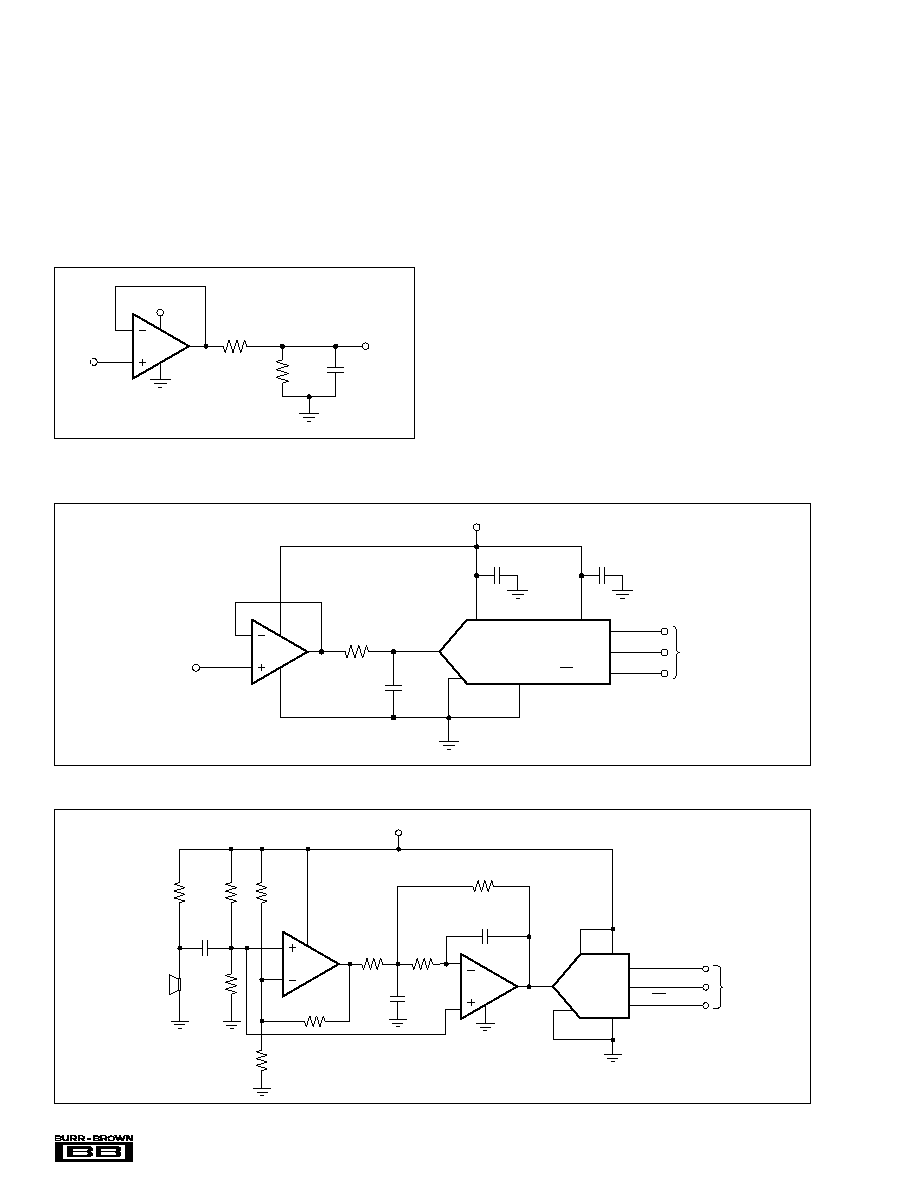
FIGURE 6. OPA342 in Noninverting Configuration Driving ADS7822.
FIGURE 7. Speech Bandpass Filtered Data Acquisition System.
DRIVING A/D CONVERTERS
The OPA342 series op amps are optimized for driving
medium-speed sampling ADCs. The OPA342 op amps buffer
the ADC's input capacitance and resulting charge injection
while providing signal gain.
Figures 6 shows the OPA342 in a basic noninverting con-
figuration driving the ADS7822. The ADS7822 is a 12-bit,
micro-power sampling converter in the MSOP-8 package.
When used with the low-power, miniature packages of the
OPA342, the combination is ideal for space-limited, low-
power applications. In this configuration, an RC network at
the ADC's input can be used to filter charge injection.
Figure 7 shows the OPA2342 driving an ADS7822 in a
speech bandpass filtered data acquisition system. This small,
low-cost solution provides the necessary amplification and
signal conditioning to interface directly with an electret
microphone. This circuit will operate with V
S
= +2.7V to
+5V with less than 500
µ
A quiescent current.
FIGURE 5. Series Resistor in Unity-Gain Configuration
Improves Capacitive Load Drive.
10
to
20
OPA342
V+
V
IN
V
OUT
R
S
R
L
C
L
C
3
33pF
V+
GND
3
1
8
4
5
6
7
≠IN
+IN
2
C
2
DCLOCK
Serial
Interface
1000pF
R
1
1.5k
R
4
20k
R
5
20k
R
6
100k
R
8
150k
R
9
510k
R
7
51k
D
OUT
V
REF
V+ = +2.7V to 5V
CS/SHDN
C
1
1000pF
Electret
Microphone
(1)
G = 100
Passband 300Hz to 3kHz
R
3
1M
R
2
1M
NOTE: (1) Electret microphone
powered by R
1
.
ADS7822
12-Bit A/D
1/2
OPA2342
1/2
OPA2342
ADS7822
12-Bit A/D
DCLOCK
D
OUT
CS/SHDN
OPA342
+5V
V
IN
V+
2
+In
3
≠In
V
REF
8
4
GND
Serial
Interface
1
0.1
µ
F
0.1
µ
F
7
6
5
NOTE: A/D Input = 0 to V
REF
V
IN
= 0V to 5V for
0V to 5V output.
RC network filters high frequency noise.
500
3300pF