 | –≠–ª–µ–∫—Ç—Ä–æ–Ω–Ω—ã–π –∫–æ–º–ø–æ–Ω–µ–Ω—Ç: OPA544 | –°–∫–∞—á–∞—Ç—å:  PDF PDF  ZIP ZIP |

©
1994 Burr-Brown Corporation
PDS-1250B
Printed in U.S.A. September, 1995
High-Voltage, High-Current
OPERATIONAL AMPLIFIER
DESCRIPTION
The OPA544 is a high-voltage/high-current opera-
tional amplifier suitable for driving a wide variety of
high power loads. High performance FET op amp
circuitry and high power output stage are combined on
a single monolithic chip.
The OPA544 is protected by internal current limit and
thermal shutdown circuits.
The OPA544 is available in industry-standard
5-lead TO-220 and 5-lead surface-mount power pack-
ages. Its copper tab allows easy mounting to a heat
sink for excellent thermal performance. It is specified
for operation over the extended industrial temperature
range, ≠40
∞
C to +85
∞
C.
Æ
OPA544
FEATURES
q
HIGH OUTPUT CURRENT: 2A min
q
WIDE POWER SUPPLY RANGE:
±
10 to
±
35V
q
SLEW RATE: 8V/
µ
s
q
INTERNAL CURRENT LIMIT
q
THERMAL SHUTDOWN PROTECTION
q
FET INPUT: I
B
= 100pA max
q
5-LEAD TO-220 PLASTIC PACKAGE
q
5-LEAD SURFACE MOUNT PACKAGE
APPLICATIONS
q
MOTOR DRIVER
q
PROGRAMMABLE POWER SUPPLY
q
SERVO AMPLIFIER
q
VALVES, ACTUATOR DRIVER
q
MAGNETIC DEFLECTION COIL DRIVER
q
AUDIO AMPLIFIER
V≠
V
O
V+
V
IN
V
IN
1 2 3 4 5
5-Lead TO-220
and
Stagger-Formed
TO-220
+
≠
Tab is connected
to V≠ supply.
V≠
V
O
V+
V
IN
V
IN
1 2 3 4 5
+
≠
Tab is connected
to V≠ supply.
5-Lead
Surface Mount
International Airport Industrial Park ∑ Mailing Address: PO Box 11400, Tucson, AZ 85734 ∑ Street Address: 6730 S. Tucson Blvd., Tucson, AZ 85706 ∑ Tel: (520) 746-1111 ∑ Twx: 910-952-1111
Internet: http://www.burr-brown.com/ ∑ FAXLine: (800) 548-6133 (US/Canada Only) ∑ Cable: BBRCORP ∑ Telex: 066-6491 ∑ FAX: (520) 889-1510 ∑ Immediate Product Info: (800) 548-6132
Æ
2
OPA544
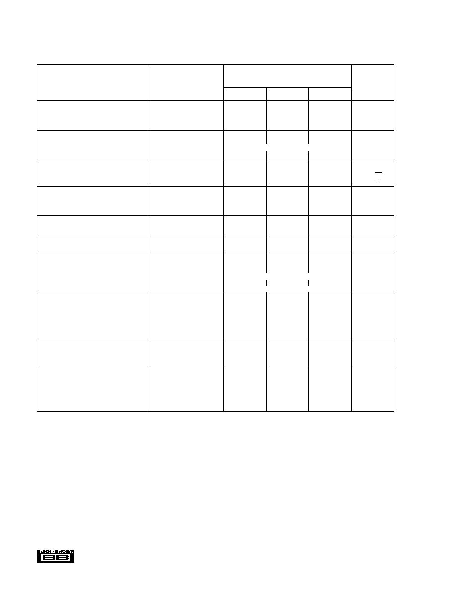
SPECIFICATIONS
At T
CASE
= +25
∞
C, V
S
=
±
35V, unless otherwise noted.
OPA544T
OPA544T-1
OPA544F
PARAMETER
CONDITION
MIN
TYP
MAX
UNITS
The information provided herein is believed to be reliable; however, BURR-BROWN assumes no responsibility for inaccuracies or omissions. BURR-BROWN assumes
no responsibility for the use of this information, and all use of such information shall be entirely at the user's own risk. Prices and specifications are subject to change
without notice. No patent rights or licenses to any of the circuits described herein are implied or granted to any third party. BURR-BROWN does not authorize or warrant
any BURR-BROWN product for use in life support devices and/or systems.
OFFSET VOLTAGE
Input Offset Voltage
±
1
±
5
mV
vs Temperature
Specified Temperature Range
±
10
µ
V/
∞
C
vs Power Supply
V
S
=
±
10V to
±
35V
±
10
±
100
µ
V/V
INPUT BIAS CURRENT
(1)
Input Bias Current
V
CM
= 0V
±
15
±
100
pA
vs Temperature
See Typical Curve
Input Offset Current
V
CM
= 0V
±
10
±
100
pA
NOISE
Input Voltage Noise
Noise Density, f = 1kHz
36
nV/
Hz
Current Noise Density, f = 1kHz
3
fA/
Hz
INPUT VOLTAGE RANGE
Common-Mode Input Range, Positive
Linear Operation
(V+) ≠6
(V+) ≠4
V
Negative
Linear Operation
(V≠) +6
(V≠) +4
V
Common-Mode Rejection
V
CM
=
±
V
S
≠6V
90
106
dB
INPUT IMPEDANCE
Differential
10
12
|| 8
|| pF
Common-Mode
10
12
|| 10
|| pF
OPEN-LOOP GAIN
Open-Loop Voltage Gain
V
O
=
±
30V, R
L
= 1k
90
103
dB
FREQUENCY RESPONSE
Gain Bandwidth Product
R
L
= 15
1.4
MHz
Slew Rate
60Vp-p, R
L
= 15
5
8
V/
µ
s
Full-Power Bandwidth
See Typical Curve
Settling Time 0.1%
G = ≠10, 60V Step
25
µ
s
Total Harmonic Distortion
See Typical Curve
OUTPUT
Voltage Output, Positive
I
O
= 2A
(V+) ≠5
(V+) ≠4.4
V
Negative
I
O
= 2A
(V≠) +5
(V≠) +3.8
V
Positive
I
O
= 0.5A
(V+) ≠4.2
(V+) ≠3.8
V
Negative
I
O
= 0.5A
(V≠) +4
(V≠) +3.1
V
Current Output
See SOA Curves
Short-Circuit Current
4
A
POWER SUPPLY
Specified Operating Voltage
±
35
V
Operating Voltage Range
±
10
±
35
V
Quiescent Current
I
O
= 0
±
12
±
15
mA
TEMPERATURE RANGE
Operating
≠40
+85
∞
C
Storage
≠40
+125
∞
C
Thermal Resistance,
JC
f > 50Hz
2.7
∞
C/W
Thermal Resistance,
JC
DC
3
∞
C/W
Thermal Resistance,
JA
No Heat Sink
65
∞
C/W
NOTES: (1) High-speed test at T
J
= 25
∞
C.

Æ
3
OPA544
Top View
ABSOLUTE MAXIMUM RATINGS
Supply Voltage, V+ to V≠ ................................................................... 70V
Output Current ................................................................. See SOA Curve
Input Voltage .................................................... (V≠) ≠0.7V to (V+) +0.7V
Operating Temperature ................................................. ≠40
∞
C to +125
∞
C
Storage Temperature ..................................................... ≠40
∞
C to +125
∞
C
Junction Temperature ...................................................................... 150
∞
C
Lead Temperature (soldering ≠10s)
(1) ...............................................................
300
∞
C
CONNECTION DIAGRAMS
NOTE: (1) Vapor-phase or IR reflow techniques are recommended for solder-
ing the OPA544F surface mount package. Wave soldering is not recommended
due to excessive thermal shock and "shadowing" of nearby devices.
V≠
V
O
V+
V
IN
V
IN
1 2 3 4 5
+
≠
Tab is connected
to V≠ supply.
5-Lead
Surface Mount
V≠
V
O
V+
V
IN
V
IN
1 2 3 4 5
5-Lead TO-220
and
Stagger-Formed
TO-220
+
≠
Tab is connected
to V≠ supply.
NOTE: (1) For detailed drawing and dimension table, please see end of data
sheet, or Appendix C of Burr-Brown IC Data Book.
ELECTROSTATIC
DISCHARGE SENSITIVITY
This integrated circuit can be damaged by ESD. Burr-Brown
recommends that all integrated circuits be handled with
appropriate precautions. Failure to observe proper handling
and installation procedures can cause damage.
ESD damage can range from subtle performance degrada-
tion to complete device failure. Precision integrated circuits
may be more susceptible to damage because very small
parametric changes could cause the device not to meet its
published specifications.
PACKAGE/ORDERING INFORMATION
PACKAGE DRAWING
PRODUCT
PACKAGE
NUMBER
(1)
OPA544T
5-Lead TO-220
315
OPA544T-1 5-Lead Stagger-Formed TO-220
323
OPA544F
5-Lead Surface-Mount
325

Æ
4
OPA544
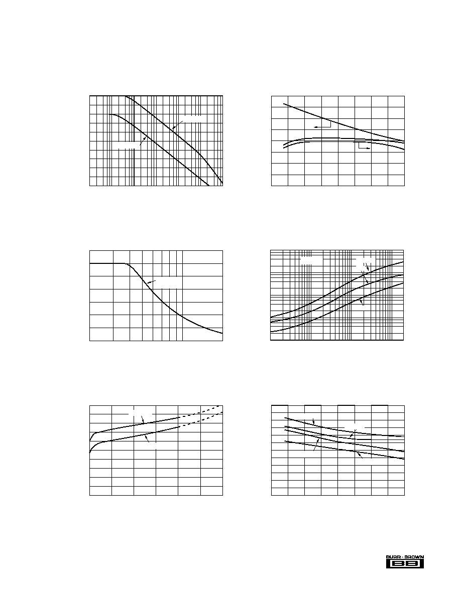
100
1k
10k
100k
1M
Common-Mode Rejection (dB)
Frequency (Hz)
COMMON-MODE REJECTION vs FREQUENCY
110
100
90
80
70
60
50
40
1
10
100
1k
10k
100k
10
Voltage Noise (nV/
Hz)
Frequency (Hz)
VOLTAGE NOISE DENSITY vs FREQUENCY
20
40
60
80
100
≠75
≠50
≠25
0
25
50
75
100
125
Quiescent Current (mA)
Temperature (∞C)
QUIESCENT CURRENT vs TEMPERATURE
13
12
11
10
9
V
S
= ±35V
V
S
= ±10V
≠75
≠50
≠25
0
25
50
75
100
125
Limit Current (A)
Temperature (∞C)
CURRENT LIMIT vs TEMPERATURE
5
4
3
2
1
0
≠75
≠50
≠25
0
25
50
75
100
125
Input Bias Current (A)
Temperature (∞C)
INPUT BIAS CURRENT vs TEMPERATURE
10n
1n
100p
10p
1p
I
OS
I
B
1
10
100
1k
10k
100k
1M
10M
Gain (dB)
Frequency (Hz)
OPEN-LOOP GAIN AND PHASE vs FREQUENCY
120
100
80
60
40
20
0
≠20
Phase (∞)
0
≠45
≠90
≠135
≠180
R
L
= 15
TYPICAL PERFORMANCE CURVES
At T
CASE
= +25
∞
C, V
S
=
±
35V, unless otherwise noted.
Æ
5
OPA544
0
1
2
3
|V
SUPPLY
| ≠ |V
OUT
| (V)
Output Current (A)
OUTPUT VOLTAGE SWING vs OUTPUT CURRENT
5
4
3
2
1
0
|(V≠) ≠V
O
|
(V+) ≠ V
O
35
30
25
20
15
10
5
0
Output Voltage (V)
MAXIMUM OUTPUT VOLTAGE vs FREQUENCY
Frequency (Hz)
20k
100k
200k
Clipping
Slew Rate
Limited
1
10
100
1k
10k
100k
1M
Power Supply Rejection (dB)
Frequency (Hz)
POWER SUPPLY REJECTION vs FREQUENCY
120
100
80
60
40
20
V+ Supply
V≠ Supply
TYPICAL PERFORMANCE CURVES
(CONT)
At T
CASE
= +25
∞
C, V
S
=
±
35V, unless otherwise noted.
≠75
≠50
≠25
0
25
50
75
100
125
|V
SUPPLY
| ≠ |V
OUT
| (V)
Temperature (∞C)
OUTPUT VOLTAGE SWING vs TEMPERATURE
6
5
4
3
2
1
0
I
O
= ≠2A
I
O
= +0.5A
I
O
= +2A
I
O
= ≠0.5A
TOTAL HARMONIC DISTORTION + NOISE
vs FREQUENCY
10
1
0.1
0.01
0.001
20
100
1k
10k 20k
THD + N (%)
Frequency (Hz)
R
L
= 15
100mW
2W
30W
≠75
≠50
≠25
0
25
50
75
100
125
Gain-Bandwidth Product (MHz)
Temperature (∞C)
GAIN-BANDWIDTH PRODUCT AND SLEW RATE
vs TEMPERATURE
2.5
2.0
1.5
1.0
0.5
Slew Rate (V/µS)
9
8
7
6
SR≠
SR+
GBW
Æ
6
OPA544
TYPICAL PERFORMANCE CURVES
(CONT)
APPLICATIONS INFORMATION
Figure 1 shows the OPA544 connected as a basic non-
inverting amplifier. The OPA544 can be used in virtually
any op amp configuration. Power supply terminals should be
bypassed with low series impedance capacitors. The tech-
nique shown, using a ceramic and tantalum type in parallel
is recommended. Power supply wiring should have low
series impedance and inductance.
The safe output current decreases as V
S
≠V
O
increases. Output
short-circuits are a very demanding case for SOA. A short-circuit
to ground forces the full power supply voltage (V+ or V≠) across
the conducting transistor. With V
S
=
±
35V the safe output current
is 1.5A (at 25∞C). The short-circuit current is approximately 4A
which exceeds the SOA. This situation will activate the thermal
shutdown circuit in the OPA544. For further insight on SOA,
consult Application Bulletin AB-039.
SAFE OPERATING AREA
Stress on the output transistors is determined by the output
current and the voltage across the conducting output transis-
tor, V
S
≠V
O
. The power dissipated by the output transistor is
equal to the product of the output current and the voltage
across the conducting transistor, V
S
≠V
O
. The Safe Operating
Area (SOA curve, Figure 2) shows the permissible range of
voltage and current.
FIGURE 1. Basic Circuit Connections.
At T
CASE
= +25
∞
C, V
S
=
±
35V, unless otherwise noted.
5V/div
G = 1+ = 3
R
2
R
1
+
Z
L
V
O
R
2
10k
R
1
5k
0.1µF
10µF
OPA544
V≠
≠35V
+35V
V+
V
IN
+
10µF
0.1µF
200MV/div
SMALL SIGNAL RESPONSE
G = 3, C
L
= 1nF
2µs/div
FIGURE 2. Safe Operating Area.
1
2
5
10
|V
S
≠ V
O
| (V)
20
50
100
SAFE OPERATING AREA
10
4
1
Output Current (A) 0.4
0.1
Current-Limited
T
C
= 25∞C
T
C
= 125∞C
T
C
= 85∞C
Output current may
be limited to less
than 4A--see text.
CURRENT LIMIT
The OPA544 has an internal current limit set for approxi-
mately 4A. This current limit decreases with increasing
junction temperature as shown in the typical curve, Current
Limit vs Temperature. This, in combination with the thermal
shutdown circuit, provides protection from many types of
overload. It may not, however, protect for short-circuit to
ground, depending on the power supply voltage, ambient
temperature, heat sink and signal conditions.
Æ
7
OPA544
POWER DISSIPATION
Power dissipation depends on power supply, signal and load
conditions. For dc signals, power dissipation is equal to the
product of output current times the voltage across the con-
ducting output transistor. Power dissipation can be mini-
mized by using the lowest possible power supply voltage
necessary to assure the required output voltage swing.
For resistive loads, the maximum power dissipation occurs
at a dc output voltage of one-half the power supply voltage.
Dissipation with ac signals is lower. Application Bulletin
AB-039 explains how to calculate or measure power dissi-
pation with unusual signals and loads.
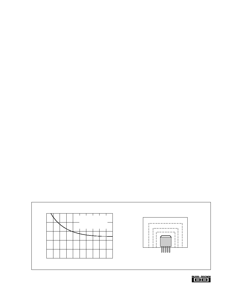
HEATSINKING
Most applications require a heat sink to assure that the
maximum junction temperature is not exceeded. The heat
sink required depends on the power dissipated and on
ambient conditions. Consult Application Bulletin AB-038
for information on determining heat sink requirements.
The mounting tab of the surface-mount package version
should be soldered to a circuit board copper area for good
heat dissipation. Figure 3 shows typical thermal resistance
from junction to ambient as a function of the copper area.
THERMAL PROTECTION
The OPA544 has thermal shutdown that protects the ampli-
fier from damage. Any tendency to activate the thermal
shutdown circuit during normal operation is indication of
excessive power dissipation or an inadequate heat sink.
The thermal protection activates at a junction temperature of
approximately 155∞C. For reliable operation, junction tem-
perature should be limited to 150∞C, maximum. To estimate
the margin of safety in a complete design (including heat
sink), increase the ambient temperature until the thermal
protection is activated. Use worst-case load and signal con-
ditions. For good reliability, the thermal protection should
trigger more than 25∞C above the maximum expected ambi-
ent condition of your application. This produces a junction
temperature of 125∞C at the maximum expected ambient
condition.
Depending on load and signal conditions, the thermal pro-
tection circuit may produce a duty-cycle modulated output
signal. This limits the dissipation in the amplifier, but the
rapidly varying output waveform may be damaging to some
loads. The thermal protection may behave differently de-
pending on whether internal dissipation is produced by
sourcing or sinking output current.
OUTPUT STAGE COMPENSATION
The complex load impedances common in power op amp
applications can cause output stage instability. Figure 3
shows an output series R/C compensation network (1
in
series with 0.01
µ
F) which generally provides excellent sta-
bility. Some variation in circuit values may be required with
certain loads.
UNBALANCED POWER SUPPLIES
Some applications do not require equal positive and negative
output voltage swing. The power supply voltages of the
OPA544 do not need to be equal. For example, a ≠6V
negative power supply voltage assures that the inputs of the
OPA544 are operated within their linear common-mode
range, and that the output can swing to 0V. The V+ power
supply could range from 15V to 65V. The total voltage (V≠
to V+) can range from 20V to 70V. With a 65V positive
supply voltage, the device may not be protected from dam-
age during short-circuits because of the larger V
CE
during
this condition.
OUTPUT PROTECTION
Reactive and EMF-generating loads can return load current
to the amplifier, causing the output voltage to exceed the
power supply voltage. This damaging condition can be
avoided with clamp diodes from the output terminal to the
power supplies as shown in Figure 4. Fast-recovery rectifier
diodes with a 4A or greater continuous rating are recom-
mended.
FIGURE 3. Thermal Resistance vs Circuit Board Copper Area.
THERMAL RESISTANCE vs
CIRCUIT BOARD COPPER AREA
50
40
30
20
10
0
Thermal Resistance,
JA
(∞C/W)
0
1
2
3
4
5
Copper Area (inches
2
)
OPA544F
Surface Mount Package
1oz copper
Circuit Board Copper Area
OPA544
Surface Mount Package

Æ
8
OPA544
FIGURE 4. Motor Drive Circuit.
G = ≠ = ≠4
R
2
R
1
1
0.01µF
R
2
20k
R
1
5k
OPA544
V≠
V+
V
IN
Motor
D
1
D
2
D
1
, D
2
: Motorola MUR420 Fast Recovery Rectifier.
OPA602
10k
OPA544
40k
0-1mA
DAC7801
12-bit
M-DAC
10V
REF102
+30V
+5V
20pF
20k
1
0.01µF
1µH
4.7k
470pF
10k
10
V
O
±20V
at 2A
Output series L/R
network helps assure
stability with very high
capacitance loads.
≠30V
+30V
8-bit
data port
(8 + 4 bits)
FIGURE 5. Digitally Programmable Power Supply.