 | –≠–ª–µ–∫—Ç—Ä–æ–Ω–Ω—ã–π –∫–æ–º–ø–æ–Ω–µ–Ω—Ç: OPA622AU | –°–∫–∞—á–∞—Ç—å:  PDF PDF  ZIP ZIP |

OPA622
FEATURES
q
LARGE SIGNAL BANDWIDTH:
150MHz (AP), 200MHz (AU)
(Voltage-Feedback)
q
HIGH OUTPUT CURRENT:
±
70mA
q
SLEW RATE: 1500V/
µ
s (AP), 1700V/
µ
s (AU)
q
DIFFERENTIAL GAIN: 0.15%
q
DIFFERENTIAL PHASE: 0.08
∞
q
EXCELLENT BANDWIDTH/SUPPLY
CURRENT RATIO: 200MHz/5mA
q
LOW INPUT BIAS CURRENT: ≠1.2
µ
A
APPLICATIONS
q
BROADCAST/HDTV EQUIPMENT
q
COMMUNICATIONS
q
PULSE/RF AMPLIFIERS
q
ACTIVE FILTER
q
HIGH SPEED ANALOG SIGNAL
PROCESSING
q
MULTIPLIER OUTPUT AMP
q
DIFFERENTIATOR FOR DIGITIZED
VIDEO SIGNALS
The feedback buffer stage provides 700MHz band-
width, a very high slew rate, and a very short signal
delay time. It is designed primarily for interstage
buffering and not for driving long cables. When com-
bined with the current-feedback amplifier section, the
OPA622 can be interconnected as a voltage-feedback
amplifier with two identical high-impedance inputs.
In this configuration, it features a low common-mode
gain, low input offset, and, due to the delay time of the
additional feedback buffer, a decrease in frequency
bandwidth compared with the current-feedback
configuration. Unlike "classical" operational amplifi-
ers, the OPA622 achieves a nearly constant bandwidth
over a wide gain and output voltage range. The
external setting of the open-loop gain with R
OG
avoids
a large compensation capacitor, improves the slew
rate, and allows a frequency response adaption to
various gains and load conditions.
International Airport Industrial Park ∑ Mailing Address: PO Box 11400 ∑ Tucson, AZ 85734 ∑ Street Address: 6730 S. Tucson Blvd. ∑ Tucson, AZ 85706
Tel: (520) 746-1111 ∑ Twx: 910-952-1111 ∑ Cable: BBRCORP ∑ Telex: 066-6491 ∑ FAX: (520) 889-1510 ∑ Immediate Product Info: (800) 548-6132
Wide-Bandwidth
OPERATIONAL AMPLIFIER
DESCRIPTION
The OPA622 is a monolithic amplifier component
designed for precision wide-bandwidth systems
including high-resolution video, RF and IF circuitry,
and communications equipment. It includes a mono-
lithic integrated current-feedback operational
amplifier block and a voltage buffer block, which,
when combined, form a voltage-feedback operational
amplifier.
When combined as a current-feedback amplifier, it
provides a 280MHz large-signal bandwidth at
±
2.5V
output level and a 1700V/
µ
s slew rate. The output
buffer stage can deliver
±
70mA output current. The
high output current capability allows the OPA622 to
drive two 50
or 75
lines with
±
3V output swing,
making it ideal along with the low differential
gain/phase errors for RF, IF, and video applications.
Æ
OPA622
OPA622
VOLTAGE-FEEDBACK
OPA622
VFA
3
4
+In
R
Q
R
1
R
IN
50
≠5V
V
IN
I
Q
Adjust
2
8
13
R
OG
9
50
R
2
V
OUT
10
≠In
BUF+
BUF≠
C
OTA
CURRENT-FEEDBACK
OPA622
CFA
4
+In
R
Q
R
IN
50
≠5V
V
IN
I
Q
Adjust
2
13
9
50
R
2
C
OTA
3
100
V
OUT
10
R
1
BUF+
© 1991 Burr-Brown Corporation
PDS-1131E
Printed in U.S.A. March, 1995
OPA622
2
Æ
SPECIFICATIONS
The information provided herein is believed to be reliable; however, BURR-BROWN assumes no responsibility for inaccuracies or omissions. BURR-BROWN assumes
no responsibility for the use of this information, and all use of such information shall be entirely at the user's own risk. Prices and specifications are subject to change
without notice. No patent rights or licenses to any of the circuits described herein are implied or granted to any third party. BURR-BROWN does not authorize or warrant
any BURR-BROWN product for use in life support devices and/or systems.
DC-SPECIFICATION
VOLTAGE-FEEDBACK AMPLIFIER (Figure 5)
At V
CC
=
±
5V, I
Q
=
±
5mA, G
CL
= +2V/V, R
LOAD
= 100
, R
SOURCE
= 50
,
R
Q
= 430
, R
OG
= 150
and T
A
= +25
∞
C, unless otherwise specified.
Power Supply Voltage .........................................................................
±
6V
Input Voltage
(1)
....................................................................
±
V
CC
to
±
0.7V
Operating Temperature ..................................................... ≠40
∞
C to +85
∞
C
Storage Temperature ...................................................... ≠40
∞
C to +125
∞
C
Junction Temperature .................................................................... +150
∞
C
Lead Temperature (soldering, 10s) ................................................ +300
∞
C
PACKAGE INFORMATION
PACKAGE DRAWING
MODEL
DESCRIPTION
NUMBER
(1)
OPA622AP
14-Pin Plastic DIP
010
OPA622AU
SO-14 Surface-Mount
235
NOTE:(1) For detailed drawing and dimension table, please see end of data
sheet, or Appendix D of Burr-Brown IC Data Book.
ABSOLUTE MAXIMUM RATINGS
NOTE: (1) Inputs are internally diode-clamped to
±
V
CC
.
ORDERING INFORMATION
MODEL
DESCRIPTION
TEMPERATURE RANGE
OPA622AP
14-Pin Plastic DIP
≠40
∞
C to +85
∞
C
OPA622AU
SO-14 Surface-Mount
≠40
∞
C to +85
∞
C
OPA622AP, AU
PARAMETER
CONDITIONS
MIN
TYP
MAX
UNITS
CLOSED-LOOP OUTPUT OFFSET VOLTAGE
Initial
1
±
15
mV
vs Temperature
210
µ
V/
∞
C
vs Supply (tracking)
V
CC
=
±
4.5V to
±
5.5V
≠46
≠50
dB
vs Supply (non-tracking)
V
CC
= +4.5V to +5.5V
≠43
dB
vs Supply (non-tracking)
V
CC
= ≠4.5V to ≠5.5V
≠51
dB
INPUT BIAS CURRENT
Initial
≠1.2
±
4
µ
A
vs Temperature
7
nA/
∞
C
vs Supply (tracking)
V
CC
=
±
4.5V to
±
5.5V
29
nA/V
vs Supply (non-tracking)
V
CC
= +4.5V to +5.5V
170
nA/V
vs Supply (non-tracking)
V
CC
= ≠4.5V to ≠5.5V
58
nA/V
OFFSET CURRENT
Input Offset Current
V
CM
= 0V
0.1
µ
A
INPUT IMPEDANCE
Differential Mode
2.4 || 1
M
|| pF
INPUT NOISE
Voltage Noise Density
f = 100kHz to 100MHz
11
nV/
MHz
Signal-to-Noise Ratio
S/N = 20 log 0.7/(V
N
∑
5MHz)
89
dB
INPUT VOLTAGE RANGE
Common-Mode Input Range
±
3.2
V
Common-Mode Rejection
V
I
= +2.5V, V
O
= 0V
78
dB
RATED OUTPUT
G
CL
= +1
Voltage Output
±
3
±
3.2
V
Closed-Loop Output Impedance
0.2
Current Output
70
mA
POWER SUPPLY
Rated Voltage
±
5
V
Derated Performance
±
4.5
±
5.5
V
Quiescent Current
R
Q
= 430
, I
O
= 0mA
±
4.4
±
5
±
5.6
mA
Quiescent Current (programmable)
Useful Range, I
O
= 0mA
3 to 8
mA
TEMPERATURE
Operating
Ambient Temperature
≠40
85
∞
C
Storage
Ambient Temperature
≠40
125
∞
C

OPA622
3
Æ
OPA622AP
OPA622AU
PARAMETER
CONDITIONS
TYP
TYP
UNITS
AC-SPECIFICATION
VOLTAGE-FEEDBACK AMPLIFIER (Figure 5)
At V
CC
=
±
5V, I
Q
=
±
5mA, G
CL
= +2V/V, R
LOAD
= 100
, R
SOURCE
= 50
,
R
Q
= 430
, R
OG
= 150
and T
A
= +25
∞
C, unless otherwise specified.
FREQUENCY DOMAIN
LARGE SIGNAL
V
O
= 2.8Vp-p, Gain = +1V/V
220
250
MHz
Closed-Loop Bandwidth (≠3dB)
V
O
= 2.8Vp-p, Gain = +2V/V
200
250
MHz
V
O
= 2.8Vp-p, Gain = +5V/V
170
230
MHz
V
O
= 2.8Vp-p, Gain = +10V/V
110
110
MHz
V
O
= 2.8Vp-p, Gain = ≠1V/V
150
250
MHz
V
O
= 2.8Vp-p, Gain = ≠2V/V
160
250
MHz
V
O
= 5.0Vp-p, Gain = +2V/V
150
200
MHz
SMALL SIGNAL BANDWIDTH
V
O
= 0.2Vp-p, Gain = +2V/V
150
170
MHz
GROUP DELAY TIME
1.4
1.4
ns
DIFFERENTIAL GAIN
f = 4.43MHz, R
LOAD
= 150
V
O
= 0.7V, Gain = +1V/V
0.12
0.12
%
V
O
= +1.4V, Gain = +2V/V
0.15
0.15
%
DIFFERENTIAL PHASE
f = 4.43MHz, R
LOAD
= 150
V
O
= 0.7V, Gain = +1V/V
0.06
0.06
Degrees
V
O
= +1.4V, Gain = +2V/V
0.08
0.08
Degrees
HARMONIC DISTORTION
Gain = +2V/V
Second Harmonic 2f
f = 10MHz, V
O
= 2.8Vp-p
≠57
≠57
dBc
Third Harmonic 3f
≠55
≠55
dBc
Second Harmonic 2f
f = 30MHz, V
O
= 2.8Vp-p
≠38
≠38
dBc
Third Harmonic 3f
≠43
≠43
dBc
Second Harmonic 2f
f = 50MHz, V
O
= 2.8Vp-p
≠33
≠33
dBc
Third Harmonic 3f
≠30
≠30
dBc
GAIN FLATNESS PEAKING
Gain = +2V/V
V
O
= 2.8Vp-p, DC to 30MHz
0.12
0.12
dB
V
O
= 2.8Vp-p, DC to 100MHz
0.3
0.3
dB
TIME DOMAIN
Rise Time
Gain = +2V/V, 10% to 90%
2.4
2.7
ns
V
O
= 5Vp-p, C
L
= 2pF
Fall Time
Gain = +2V/V, 10% to 90%
3.5
3.2
ns
V
O
= 5Vp-p, C
L
= 2pF
SLEW RATE
Gain = +2V/V, Rise Time = 2ns
V
O
= 6.2Vp-p
Positive
1500
1700
V/
µ
s
Negative
1300
1600
V
µ
s
SETTLING TIME
Gain = +2V/V, Rise Time = 2ns
V
O
= 2Vp-p, 0.1%
17
17
ns
OPA622
4
Æ
PAD
FUNCTION
1
Quiescent Current Adjustment
2
Inverting Analog Input
3
Non-Inverting Analog Input
4
NC
5
NC
6
≠5V Supply
7
≠5V Supply, Output
8
Inverting Buffer Output
9
Analog Output
10
Analog OTA Output
11
+5V Supply, Output
12
+5V Supply
13
Non-Inverting Buffer Output
Substrate Bias: Negative Supply
NC: No Connection
Wire Bonding: Gold wire bonding is recommended.
DICE INFORMATION
MECHANICAL INFORMATION
MILS (0.001")
MILLIMETERS
Die Size
57 x 69
±
5
1.44 x 1.76
±
0.13
Die Thickness
14
±
1
0.55
±
0.025
Min. Pad Size
4 x 4
0.10 x 0.10
Backing: Titanium
0.02+0.05,≠0.0
0.0005+0.0013, ≠0.0
Gold
0.30
±
0.05
0.0076
±
0.0013
OPA622AD DIE TOPOGRAPHY
PIN NO.
DESCRIPTION
FUNCTION
1
NC
No Connection
2
I
Q
Adjust
Quiescent Current Adjustment; typical 3-8mA
3
≠In
Inverting Analog Input
4
+In
Noninverting Analog Input
5
≠V
CC
Negative Supply Voltage; typical ≠5VDC
6
≠V
CC OUT
Negative Supply Voltage Output Buffer;
typical ≠5VDC
8
BUF≠
Analog Output Feedback Buffer
9
V
OUT
Analog Output
10
OTA
Analog Output OTA
11
+V
CC OUT
Positive Supply Voltage Output Buffer; typical
+5VDC
12
+V
CC
Positive Supply Voltage; typical +5VDC
13
BUF+
Analog Output/Input
14
NC
No Connection
PIN CONFIGURATION
FUNCTIONAL DESCRIPTION
NC
I
Q
Adjust
≠In
+In
≠V
CC
≠V
CC OUT
NC
NC
BUF+
+V
CC
+V
CC OUT
OTA
V
OUT
BUF≠
1
2
3
4
5
6
7
OPA622
14
13
12
11
10
9
8
FB
OTA
OB
13
4
10
3
5
12
2
Biasing
11
6
8
SO/DIP
9
Top View
ELECTROSTATIC
DISCHARGE SENSITIVITY
Electrostatic discharge can cause damage ranging from per-
formance degradation to complete device failure. Burr-
Brown Corporation recommends that all integrated circuits
be handled and stored using appropriate ESD protection
methods.
ESD damage can range from subtle performance degrada-
tion to complete device failure. Precision integrated circuits
may be more susceptible to damage because very small
parametric changes could cause the device not to meet
published specifications.
OPA622
5
Æ
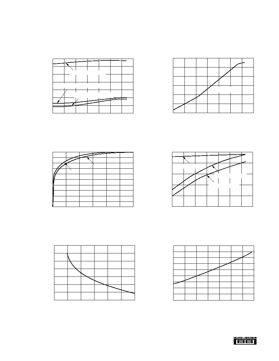
QUIESCENT CURRENT vs TEMPERATURE
9
8
7
6
5
4
3
2
1
0
≠40
≠20
0
20
40
60
80
100
Quiescent Current (mA)
Temperature (∞C)
QUIESCENT CURRENT vs R
Q
RESISTANCE
9
8
7
6
5
4
3
2
0
200
400
600
800
1000
1200
R
Q
(
)
Quiescent Current (mA)
INPUT STAGE OFFSET VOLTAGE vs TEMPERATURE
0.5
0
≠0.5
≠1
≠1.5
≠2
Temperature (∞C)
Offset Voltage Drift (mv)
≠40
≠20
0
20
40
60
80
100
Positive Input Voltage
Negative Input Voltage
Input Offset Voltage
INPUT OFFSET VOLTAGE vs TIME
100
90
80
70
60
50
40
30
20
10
0
V
OS
(% final value)
Time (minutes)
0
1
2
3
4
5
6
DIP
SO-14
INPUT BIAS CURRENT vs TEMPERATURE
0
≠0.2
≠0.4
≠0.6
≠0.8
≠1
≠1.2
≠1.4
Input Bias Current (µA)
Temperature (∞C)
≠40
≠20
0
20
40
60
80
100
Negative Input Bias Current
Input Bias Offset Current
Positive Input Bias Current
TYPICAL PERFORMANCE CURVES
VOLTAGE-FEEDBACK AMPLIFIER (Figure 5)
At V
CC
=
±
5V, I
Q
=
±
5mA, G
CL
= +2V/V, R
LOAD
= 100
, R
SOURCE
= 50
,
R
Q
= 430
, R
OG
= 150
and T
A
= +25
∞
C, unless otherwise specified.
CLOSED-LOOP OUTPUT OFFSET VOLTAGE
vs TEMPERATURE
15
10
5
0
≠5
≠10
≠15
Temperature (∞C)
Offset Voltage (mV)
≠40
≠20
0
20
40
60
80
100
G
CL
= +2V/V
OPA622
6
Æ
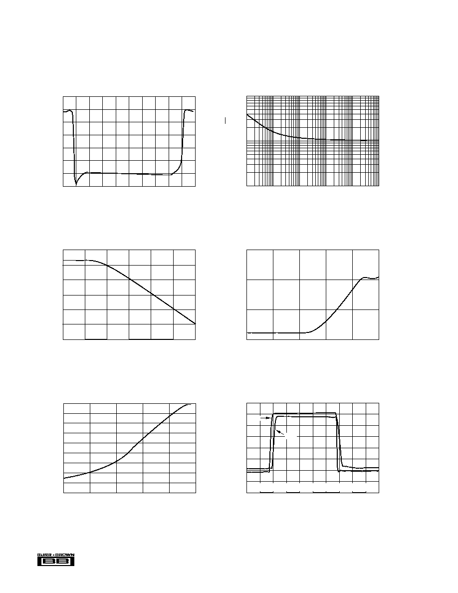
TYPICAL PERFORMANCE CURVES
(CONT)
VOLTAGE-FEEDBACK AMPLIFIER (Figure 5)
At V
CC
=
±
5V, I
Q
=
±
5mA, G
CL
= +2V/V, R
LOAD
= 100
, R
SOURCE
= 50
,
R
Q
= 430
, R
OG
= 150
and T
A
= +25
∞
C, unless otherwise specified.
INPUT IMPEDANCE vs FREQUENCY
10M
1M
100k
10k
1k
100
10
Input Impedance (
)
Frequency (Hz)
1k
10k
100k
1M
10M
100M
1G
SPECTRAL NOISE VOLTAGE DENSITY
100
10
1
100
1k
10k
100k
1M
10M
Frequency (Hz)
Voltage Noise nV/
Hz
OUTPUT IMPEDANCE vs FREQUENCY
Frequency (Hz)
10k
100k
1M
10M
100M
1G
100
10
1
100m
Output Impedance (
)
G
CL
= +2
OVERLOAD RECOVERY CHARACTERISTICS
Time (ns)
3
2.25
1.5
0.75
0
≠0.75
≠1.5
≠2.25
≠3
Input Voltage (V)
0
10
20
30
40
50
60
70
80
90
100
6
4.5
3
1.5
0
≠1.5
≠3
≠4.5
≠6
Output Voltage (V)
V
OUT
V
IN
G
CL
= +2V/V, V
IN
= 3.75Vp-p, t
RISE
= t
FALL
= 1ns (Generator)
COMMON-MODE REJECTION
vs COMMON-MODE INPUT VOLTAGE
Common-Mode Input Voltage (V)
≠5
≠4
≠3
≠2
≠1
0
1
2
3
4
5
≠5
≠55
≠60
≠65
≠70
≠75
≠80
≠85
Common-Mode Rejection (dB)
COMMON-MODE REJECTION vs FREQUENCY
0
≠10
≠20
≠30
≠40
≠50
≠60
≠70
≠80
≠90
10k
100k
1M
10M
100M
1G
Frequency (Hz)
Common-Mode Rejection (dB)

OPA622
7
Æ
TYPICAL PERFORMANCE CURVES
(CONT)
VOLTAGE-FEEDBACK AMPLIFIER (Figure 5)
At V
CC
=
±
5V, I
Q
=
±
5mA, G
CL
= +2V/V, R
LOAD
= 100
, R
SOURCE
= 50
,
R
Q
= 430
, R
OG
= 150
and T
A
= +25
∞
C, unless otherwise specified.
SMALL SIGNAL PULSE RESPONSE
Time (ns)
160
120
80
40
0
≠40
≠80
≠120
≠160
Output Voltage (mV)
0
10
20
30
40
50
60
70
80
90
100
G
CL
= +1V/V, V
OUT
= 0.2Vp-p, t
RISE
= t
FALL
= 1ns (Generator)
SMALL SIGNAL PULSE RESPONSE
Time (ns)
160
120
80
40
0
≠40
≠80
≠120
≠160
Output Voltage (mV)
0
10
20
30
40
50
60
70
80
90
100
G
CL
= +10V/V, V
OUT
= 0.2Vp-p, t
RISE
= t
FALL
= 1ns (Generator)
15
10
5
0
≠5
≠10
≠15
≠20
≠25
1M
10M
100M
1G
Frequency (Hz)
Output Voltage (Vp-p)
BANDWIDTH vs OUTPUT VOLTAGE
20
dB
300k
G
CL
= +2V/V
0.2Vp-p
0.6Vp-p
1.4Vp-p
2.8Vp-p
5Vp-p
15
10
5
0
≠5
≠10
≠15
≠20
≠25
1M
10M
100M
1G
Frequency (Hz)
Output Voltage (Vp-p)
BANDWIDTH vs OUTPUT VOLTAGE
20
dB
300k
0.2Vp-p
1.4Vp-p
2.8Vp-p
5Vp-p
G
CL
= +1V/V
0.6Vp-p
3G
LARGE SIGNAL PULSE RESPONSE
Time (ns)
2.5
0
≠2.5
Input/Output Voltage (V)
0
10
20
30
40
50
60
70
80
90
100
G = +1V/V, V
OUT
= 5Vp-p, t
RISE
= t
FALL
= 1ns (Generator)
V
OUT
V
IN
LARGE SIGNAL PULSE RESPONSE
Time (ns)
2.5
0
≠2.5
Output Voltage (V)
0
10
20
30
40
50
60
70
80
90
100
G
CL
= +10V/V, V
OUT
= 5Vp-p, t
RISE
= t
FALL
= 1ns (Generator)
OPA622
8
Æ
15
10
5
0
≠5
≠10
≠15
≠20
≠25
1M
10M
100M
1G
Gain (dB)
BANDWIDTH vs R
LOAD
20
dB
100k
G = +2V, V
OUT
= 2.8Vp-p for all load resistances
500
100
50
200
1M
10M
100M
1G
Frequency (Hz)
Gain (5dB/Div)
FREQUENCY RESPONSE vs C
LOAD
G
CL
= +2V/V, V
OUT
= 2.8Vp-p
10pF
22pF
47pF
C
LOAD
R
OG
C
OTA
10p180
0.5p
22p200
0.5p
47p150
0.5p
100k
15
10
5
0
≠5
≠10
≠15
≠20
≠25
1M
10M
100M
1G
Frequency (Hz)
Output Voltage (Vp-p)
BANDWIDTH vs OUTPUT VOLTAGE
20
dB
300k
G
CL
= ≠1V/V
0.2Vp-p
0.6Vp-p
1.4Vp-p
2.8Vp-p
5Vp-p
TYPICAL PERFORMANCE CURVES
(CONT)
VOLTAGE-FEEDBACK AMPLIFIER (Figure 5)
At V
CC
=
±
5V, I
Q
=
±
5mA, G
CL
= +2V/V, R
LOAD
= 100
, R
SOURCE
= 50
,
R
Q
= 430
, R
OG
= 150
and T
A
= +25
∞
C, unless otherwise specified.
3
2
1
0
≠1
≠2
≠3
≠4
≠5
1M
10M
100M
1G
Frequency (Hz)
Gain (dB)
GAIN FLATNESS
4
≠6
300k
G
CL
= +2V/V, V
OUT
= 0.2Vp-p
15
10
5
0
≠5
≠10
≠15
≠20
≠25
1M
10M
100M
1G
Frequency (Hz)
Output Voltage (Vp-p)
BANDWIDTH vs OUTPUT VOLTAGE
20
dB
100k
G
CL
= ≠2V/V
0.2Vp-p
0.6Vp-p
1.4Vp-p
2.8Vp-p
5Vp-p
15
10
5
0
≠5
≠10
≠15
≠20
≠25
1M
10M
100M
1G
Frequency (Hz)
Output Voltage (Vp-p)
BANDWIDTH vs OUTPUT VOLTAGE
20
dB
300k
G
CL
= +10V/V
0.2Vp-p
0.6Vp-p
1.4Vp-p
2.8Vp-p
5Vp-p
OPA622
9
Æ
4
2
0
≠2
≠4
300k
1M
10M
100M
1G
Frequency (Hz)
GROUP DELAY TIME vs FREQUENCY
Group Delay Time (ns)
Group Delay Time
V
IN
V
OUT
150
50
G
CL
= +2V/V
DUT
TYPICAL PERFORMANCE CURVES
(CONT)
VOLTAGE-FEEDBACK AMPLIFIER (Figure 5)
At V
CC
=
±
5V, I
Q
=
±
5mA, G
CL
= +2V/V, R
LOAD
= 100
, R
SOURCE
= 50
,
R
Q
= 430
, R
OG
= 150
and T
A
= +25
∞
C, unless otherwise specified.
GAIN ERROR vs INPUT VOLTAGE
35
30
25
20
15
10
5
0
Input Voltage (V)
≠5
≠4
≠3
≠2
≠1
0
1
2
3
4
5
Gain Error (%)
TRANSFER FUNCTION
≠5
5
4
3
2
1
0
≠1
≠2
≠3
≠4
≠5
Input Voltage (V)
≠4
≠3
≠2
≠1
0
1
2
3
4
5
Output Voltage (V)
OUTPUT BIAS CURRENT vs TEMP
8
6
4
2
0
≠2
≠4
≠6
≠8
≠10
≠40
≠20
0
20
40
60
80
100
Output Bias Current (µA)
Temperaure (∞C)
0
≠10
≠20
≠30
≠40
≠50
≠60
≠70
Frequency (Hz)
HARMONIC DISTORTION vs FREQUENCY
≠80
100k
1M
10M
100M
Harmonic Distortion (dBc)
2f
3f
G
CL
= +2V/V, V
OUT
= 2.8Vp-p, R
LOAD
= 100
OPA622
10
Æ
INPUT PROTECTION
The need for protection from static damage has long been
recognized for MOSFET devices, but all semiconductor
devices deserve protection from this potentially damaging
source. The OPA622 incorporates on-chip ESD protection
diodes as shown in Figure 1. These diodes eliminate the
need for external protection diodes, which can add capaci-
tance and degrade AC performance.
the amplifier input characteristics without necessarily
destroying the device. In precision amplifiers, such changes
may degrade offset and drift noticeably. For this reason,
static protection is strongly recommended when handling the
OPA622.
DISCUSSION
OF PERFORMANCE
The OPA622 provides full-power bandwidth previously
unattainable in monolithic devices. In addition, the amplifier
operates with reduced quiescent. The flexibility of the
OPA622 design provides the speed advantages of a current-
feedback amplifier or the precision advantages of a voltage-
feedback amplifier. The programmable quiescent current
feature also helps to adapt the amplifier to the particular
design requirements.
Figure 2 shows the simplified circuit diagram of the OPA622.
It contains four major sections: the bias circuitry, the OTA,
the output buffer, and the feedback buffer.
BIAS CIRCUITRY
The bias circuitry controls the quiescent current of the signal
processing stages, allows external quiescent current setting
using the resistor R
Q
connected from Pin 2 to ≠V
CC
, sets the
amplifier's transconductance, and, with its temperature
characteristics, maintains a constant transconductance over
temperature. The quiescent current controls the small-signal
bandwidth and AC behavior. The OPA622 is specified with
a quiescent current of
±
5mA with R
Q
= 430
. The recom-
mended range is
±
3mA to
±
8mA.
+V
CC
≠V
CC
ESD Protection diodes internally
connected to all pins.
Internal
Circuitry
External
Pin
FIGURE 1. Internal ESD Protection.
As shown, all input pins of the OPA622 are protected from
ESD internally by a pair of back-to-back reverse-biased
diodes to either power supply. These diodes begin to con-
duct when the input voltage exceeds either power supply by
about 0.7V. This situation can occur when the amplifier
loses its power supplies while a signal source is still present.
The diodes can typically withstand a continuous current of
30mA without destruction. To ensure long-term reliability,
however, the diode current should be limited externally to
approximately 10mA whenever possible.
The internal protection diodes are designed to withstand
2.5kV (using the Human Body Model) and will provide
adequate ESD protection for most normal handling proce-
dures. However, static damage can cause subtle changes in
R
OG
13
12
+V
CC
2
+In 4
8
12
I
Q
Adjust
≠V
CC
R
Q
(ext.)
100
5
+ BUF ≠
3
≠ In
9
4
V
OUT
≠V
CC OUT
6
11
+V
CC OUT
OTA
10
Bias
Circuitry
OTA
FB
OB
FIGURE 2. Simplified Circuit Diagram.
OPA622
11
Æ
Application circuits generally do not show the resistor
R
Q
, but it is required for proper operation.
With a fixed R
Q
, the quiescent current increases with tem-
perature (see Typical Performance Curves.) This variation
of the quiescent current with temperature keeps the band-
width and AC behavior relatively constant with temperature.
It is also possible to vary the quiescent current by an external
control signal or circuitry. Figure 3 shows a circuit to disable
the OPA622 with TTL-compatible logic levels. 0V/5V logic
levels are converted into a 1mA/0mA current connected to
Pin 2. The current flowing in R
Q
increases the voltage at Pin
2 to approximately 1V above the ≠V
CC
rail, thus reducing I
Q
to near zero and disabling the OPA622.
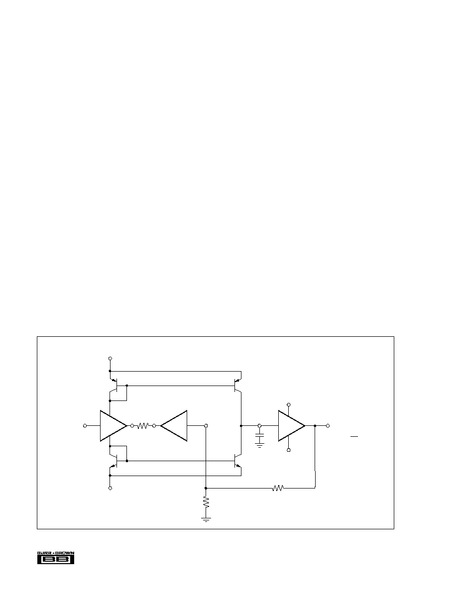
OTA AND OUTPUT BUFFER SECTIONS
An Operational Transconductance Amplifier (OTA) and an
output buffer are the basic building blocks of a current-
feedback amplifier. The current-feedback configuration of
the OPA622 is illustrated in Figure 4. The OTA consists of
a complementary emitter follower and a subsequent comple-
mentary current mirror. The voltage at the high-impedance
+In terminal is transferred to the BUF+ input/output termi-
nal at a low impedance. If a current flows into or out of the
BUF+ terminal, the complementary mirror reflects the
current to the OTA terminal. The current flow at the high-
impedance OTA terminal is determined by the product of
the voltage between the +In and BUF+ terminals and the
transconductance. The output buffer section is an open-loop
buffer consisting of complementary emitter followers. It is
designed to drive cables or low-impedance loads. The buffer
output is not current-limited or -protected. As can be seen in
Figure 4, the feedback network for a current-feedback
amplifier is applied between the V
OUT
and BUF+ terminals.
Figure 8 illustrates the bandwidth for various output volt-
ages of the current feedback configuration.
FIGURE 3. Logic-Controlled Disable Circuit.
FIGURE 4. Current-Feedback Amplifier.
100k
100
R
Q
430
≠5V
Internal
Current Source
Circuitry
OPA622
2N2907
+5V
0/5V
Logic In
5V: OPA622 On
2
5
I
C
I
C
= 0: OPA622 On
I
C
= 1mA: OPA622 Off
4.7k
C
OTA
9
6
11
≠V
CC OUT
V
OUT
+ V
CC OUT
R
1
R
2
10
13
12
+V
CC
5
≠V
CC
+In
4
BUF+
OTA
OB
FEEDBACK BUFFER SECTION
This section of the OPA622 is a complementary emitter
follower identical to the input buffer of the OTA section. It
is designed for interstage buffering, not for driving long
cables or low-impedance loads. A minimum load resistance
of 500
is recommended when using the feedback buffer as
a stand-alone device. The feedback buffer output is not
current-limited or -protected. The bandwidth of the feedback
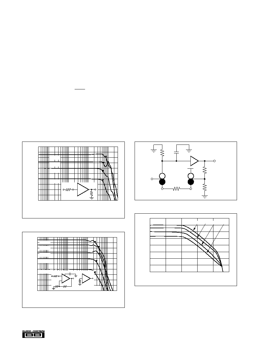
buffer is shown in Figure 7.
OPA622
12
Æ
CONFIGURATIONS
VOLTAGE-FEEDBACK AMPLIFIER
The OPA622's internal design differs from a "classical"
operational amplifier structure, but it can nevertheless be
used in all traditional operational amplifier applications. As
with conventional op amps, the feedback network connected
to the inverting input controls closed-loop gain (G
CL
). But
with the OPA622, the resistor R
OG
is simultaneously adapted
to the closed-loop gain, optimizing the frequency response
and stability.
The "classical" differential input stage consists of two
identical transistors with an emitter degeneration resistor,
two current sources, and an active load diode. However, the
classical configuration limits the current through the gain
transistor to that supplied by the current sources.
In the new design, a complementary push-pull buffer (emit-
ter follower) replaces one side of the differential stage
without the 0.7V offset. The feedback buffer as a second
complementary emitter follower and the open-loop gain
resistor R
OG
connected between the outputs recreate the
differential stage without the disadvantages of the classical
design. The current charging the parasitic capacitance at the
base of the gain transistor is no longer limited to the fixed
current of the current sources and is proportional to the input
signal. This improvement results in an approximately
10-times better slew rate.
The amplified current through the gain transistor of one of
the buffers is mirrored and becomes the output current. The
high-impedance output of the OTA is now buffered by the
high current output stage, which is designed to drive long
cables or low-impedance loads at full power.
The identical input buffers reduce the input offset to typi-
cally less than
±
7
µ
V. Closed-loop output offset is typically
due to mismatch of the NPN and PNP transistors in the OTA
mirror
±
100
µ
V after the output bias current is trimmed.
Figure 5 illustrates the circuit configuration of the voltage-
feedback op amp in a complementary circuit design. The
feedback buffer and the OTA input buffer form the
differential input. Inserting the feedback buffer section trans-
forms the current feedback shown in Figure 4 into the
voltage feedback shown in Figure 5.
The resistor R
OG
sets the open-loop gain and corresponds to
the emitter degeneration resistor in a classical differential
stage. Because the R
OG
resistor can be varied externally, a
flat frequency response can be achieved over a wide range
of applications without the need to compensate the amplifier
with a capacitor. In contrast to a current-feedback amplifier,
it is possible to adjust the closed-loop gain using the
feedback resistors and to adjust the open-loop gain indepen-
dently using R
OG
to optimize the frequency response.
Unlike "classical" operational amplifier structures, the
OPA622 configuration makes it possible to attain a nearly
constant bandwidth for varying closed-loop gains, as well as
improved frequency response and large-signal behavior. In
addition--and also unlike current-feedback op amps--it
provides two identical high-impedance inputs, lower input
offset values, and improved CMRR.
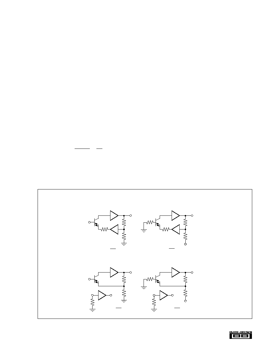
CURRENT-FEEDBACK AMPLIFIER
Figure 4 shows the current-feedback configuration. The
feedback loop is closed from the output to the BUF+
terminal of the OTA section. The shorter feedback loop
FIGURE 5. Voltage-Feedback Amplifier.
9
6
11
V
OUT
+ V
CC OUT
R
1
10
+In
≠ V
CC OUT
OB
FB
R
OG
R
2
C
OTA
≠In
3
8
13
≠ V
CC
+ V
CC
4
OTA
5
12
C
OTA
: Sets the first open-loop pole
R
OG
: Sets the open-loop gain
G
CL
= 1 +
R
2
R
1
OPA622
13
Æ
FIGURE 6. Op Amp Configurations for OPA622.
Amplifiers with an external compensation capacitor allow
optimal frequency adjustment versus closed-loop gain, but
nevertheless do not significantly improve large-signal be-
havior. The most effective solution is to make the open-loop
gain (G
OL
) externally adjustable.
The widely-used current-feedback op amp type designed
with real complementary circuit techniques overcomes the
internal compensation capacitor and allows the feedback
network to set the open-loop gain. The ratio of the feedback
resistors determines the low-frequency closed-loop gain,
and the parallel impedance defines the amplifier's open-loop
gain for stable operation and flat frequency response. A
nearly constant bandwidth can be achieved over a wide
range of closed-loop gains. However, current-feedback op
amps suffer from nonidentical inputs and poor input offset
and CMRR. The voltage-feedback op amp OPA622 with its
complementary topology features two identical high-imped-
ance inputs, lower input offset values, and improved CMRR.
The ratio of the feedback resistors determines the low-
frequency closed-loop gain, and the external resistor R
OG
sets the open-loop gain to achieve a flat frequency response
over a wide range of closed-loop gains. Since R
OG
can be
selected, optimized pulse responses are possible even with
larger load capacitances. The OPA622 combines the slew
rate enhancements of a complementary amplifier design
with the precision of a voltage-feedback system.
The hybrid model shown in Figure 9 describes the AC
behavior of a noncompensated wide-band differential op
amp. The open-loop frequency response, which is illustrated
in Figure 10 for various R
OG
values, is determined by two
without the feedback buffer produces the wider bandwidth
of the current-feedback concept. The additional signal delay
time through the feedback buffer determines the difference
in AC performance between voltage and current feedback.
The specifications for offset voltage, CMMR, and settling
times are the compromise for higher speed.
The open-loop gain for the current-feedback amplifier varies
directly with the closed-loop gain and can be adjusted by
changing the size of R
2
||R
1
. For gains of less than 10V/V,
the open-loop gain can be adjusted to achieve bandwidth
independent of gain, but the effects of this adjustment
become limited when second-order effects start to dominate.
Figure 6 gives an overview of the OPA622 inverting and
non-inverting amplifier configurations and shows the equa-
tions for the closed-loop gains.
OPTIMAL FREQUENCY RESPONSE ADJUSTMENT
Conventional voltage-feedback op amps use a compensation
capacitor for stable unity-gain operation. During transitions,
the quiescent current charges and discharges this capacitor,
and both parameters determine the slew rate according to:
SR = =
This method is not appropriate for wide-band op amps. The
slew rate and thus the large-signal behavior are significantly
reduced, and the bandwidth decreases with increasing closed-
loop gains according to the gain-bandwidth product.
t
C
I
V
OUT
≠V
IN
FB
OB
R
2
R
1
G
CL
= 1 +
R
1
R
2
R
OG
+V
IN
FB
OB
R
2
R
1
G
CL
= ≠
R
1
R
2
R
OG
V
OUT
Voltage-Feedback
OB
R
2
R
1
G
CL
= 1 +
R
1
R
2
+V
IN
OB
R
2
R
1
V
OUT
≠V
IN
Current-Feedback
FB
G
CL
= ≠
R
1
R
2
FB
Non-inverting
Inverting
Non-inverting
Inverting
V
OUT
V
OUT
OTA
OTA
OTA
OTA
OPA622
14
Æ
gain) at low closed-loop gains. Harmonic distortion is also
improved with increased open-loop gain. Figure 12 shows the
OPA622 frequency response at G
CL
= +2V/V and variable
R
OG
to demonstrate its influence on a flat frequency response.
Slight variation of R
OG
might be necessary to compensate for
load capacitance. It is possible to achieve optimal pulse
response over a wide range of load capacitances without
overshooting and ringing. As an example, Figure 13 shows a
selection curve for the optimal R
OG
value versus the load
capacitance at a gain (G
CLO
) of +2V/V.
THERMAL CONSIDERATIONS
The OPA622 does not require a heat sink for operation in
most environments. A heat sink will, however, reduce the
internal thermal rise, resulting in cooler, more reliable
operation. At extreme temperatures and under full load
conditions, a heat sink is necessary. The internal power
dissipation is given by the equation P
D
= P
DQ
+ P
DL
, (P
DQ
is
the quiescent power dissipation and P
DL
is the power dissi-
pation in the output stage due to the load). Although the P
DQ
is very low (50mW at V
CC
=
±
5V), care should be taken
FIGURE 8. Bandwidth vs Output Voltage (Current-Feedback
Amplifier).
≠1
R
2
R
1
R
OG
g
m
g
m
+In
4
13
8
10
3
9
R
T
C
T
V
OUT
T
D
≠In
FIGURE 9. Hybrid Model of a Wideband Op Amp.
FIGURE 10. Open-Loop Gain vs R
OG
.
60
50
40
30
20
10
0
≠10
≠20
Gain (dB)
Frequency (Hz)
10k
100k
1M
10M
100M
1G
0
27
150
390
R
OG
=
20
15
10
5
0
≠5
≠10
≠15
≠20
≠25
dB
Output Voltage (Vp-p)
Frequency (HZ)
1M
10M
100M
1G
3G
0.6Vp-p
2.8Vp-p
1.4Vp-p
0.2Vp-p
150
8
+1
1k
20
15
10
5
0
≠5
≠10
≠15
≠20
≠25
dB
Output Voltage (Vp-p)
Frequency (HZ)
1M
10M
100M
1G
3G
0.6Vp-p
2.8Vp-p
1.4Vp-p
0.2Vp-p
5.0Vp-p
150
9
+1
150
8
180
180
0.5pF
10
+
13
3
≠
4
G
CL
= +2V/V
FIGURE 7. Bandwidth vs Output Voltage (Feedback Buffer ).
time constants. The elements R and C
OTA
between the
current source output and the output buffer form the first
open-loop pole T
C
. The signal delay time, T
D,
modelled in
the output buffer, combines several small phase-shifting
time constants and delay times. They are distributed through-
out the amplifier and are also present in the feedback loop.
As shown in Figure 10, an increasing R
OG
leads to a
decreasing open-loop gain. The ratio of the two time con-
stants, T
C
and T
D
, of the open-loop frequency response also
determines the product G
OL
∑ G
CL
for optimal closed-loop
frequency response.
G
OL
= G
+
CL
∑
T
C
and T
D
are fixed by the op amp design. The purpose of R
OG
now is to vary G
OL
versus G
CL
to keep the product G
OL
∑ G
CL
constant, which is the theoretical condition for optimal and
gain-independent frequency response. Figure 11 summarizes
some optimal flat closed-loop responses and indicates the R
OG
values. It should be noted that the bandwidth remains rela-
tively constant and R
OG
has its highest value (low open-loop
T
C
2T
D
OPA622
15
Æ
when a signal is applied. For high-speed op amps, a more
precise approach to determine power consumption is to
measure the average total quiescent current for several
typical load conditions. The power consumption of the
OPA622 is influenced by the signal type and frequency, the
output voltage and load resistor, and the repetition rate of the
signal transitions. Figure 14 shows the total average supply
current versus the frequency of an applied sine wave for
various output voltages. Figure 15 illustrates the total
quiescent current versus the repetition frequency of an
applied square wave signal.
CIRCUIT LAYOUT
The high-frequency performance of the OPA622 can be
greatly affected by the physical layout of the printed circuit
board. The following tips are offered as suggestions, not as
absolute musts. Oscillations, ringing, poor bandwidth and
settling, and peaking are all typical problems that plague
high-speed components when they are used incorrectly.
∑ Bypass power supplies very close to the device pins. Use
tantalum chip capacitors (approximately 2.2
µ
F) and a
parallel 470pF ceramic chip capacitor. Surface-mount types
are recommended because of their low lead inductance.
∑ PC board traces for power lines should be wide to reduce
impedance.
∑ Make short, low-inductance traces. The entire physical
circuit should be as small as possible.
∑ Use a low-impedance ground plane on the component side
to ensure that low-impedance ground is available through-
out the layout.
∑ Place the R
OG
resistor as close as possible to the package
and use the shortest possible trace length.
∑ Do not extend the ground plane over high-impedance
nodes sensitive to stray capacitances such as the amplifier's
input and R
OG
terminals.
∑ Sockets are not recommended, because they add signifi-
cant inductance and parasitic capacitance. If sockets are
required, use zero-profile solderless sockets.
∑ Use low-inductance, surface-mount components for
best AC performance.
∑ A resistor (50
to 330
) in series with the high-imped-
ance inputs is strictly recommended for stable operation.
∑ Plug-in prototype boards and wire-wrap boards will not
function well. A clean layout using RF techniques is
essential.
FIGURE 11. Optimum Response vs Closed-Loop Gains.
FIGURE 12. Closed-Loop Gain vs R
OG
.
10
5
0
≠5
≠10
≠15
≠20
≠25
Amplitude (dB)
Frequency (Hz)
100k
1M
10M
100M
1G
R
OG
= 50
R
OG
= 150
R
OG
= 300
G
CL
= +2V/V
15
10
5
0
≠5
≠10
≠15
≠20
≠25
1M
10M
1M
1G
Frequency (Hz)
Gain (5dB/Div)
20
≠30
R
OG
= 10
100k
R
OG
= 150
R
OG
= 390
R
OG
= 200
R
OG
= 120
G
CL
= +10
G
CL
= +2
G
CL
= +1
G
CL
= ≠1
G
CL
= ≠2
OPA622AP
V
O
= 1.4Vp-p, Refer to Table I for
recommended component values.
FIGURE 14. Average Supply Current vs Frequency (Sine Wave).
FIGURE 13. Bandwidth vs C
LOAD
.
1M
10M
100M
1G
Frequency (Hz)
Gain (5dB/Div)
G
CL
= +2V/V, V
O
= 2.8Vp-p
10pF
22pF
47pF
C
LOAD
R
OG
C
OTA
10p180
0.5p
22p200
0.5p
47p150
0.5p
50
40
30
20
10
0
Frequency (Hz)
Average Supply Current (mA)
300k
1M
10M
100M
1G
G = +2V/V, R
LOAD
= 100
5Vp-p
2.8Vp-p
1.4Vp-p
0.2Vp-p
OPA622
16
Æ
FIGURE 16. Test Circuit Schematic.
FIGURE 15. Average Supply Current vs Frequency (Square Wave).
R
QC
390
2
4
3
R
4
NC
(1)
5
+V
CC OUT
10
11
9
OB
Out
R
1
330
6
≠V
CC OUT
13
8
R
OG
150
FB
OTA
OPA622
R
3
0
C
OTA
≠V
CC
Z
O
= 50
R
5
NC
(1)
R
IN
50
1pF
Biasing
R
6
NC
(1)
R
SOURCE
= 50
NC
(1)
Z
O
= 50
R
SOURCE
= 50
R
L2
100
R
L1
100
R
ING
NC
(1)
R
LR
150
Z
O
= 50
In
POS
In
NEG
R
2
330
12
≠V
CC
+V
CC
C
1
C
2
+5V
C
6
C
5
R
9
10
R
8
10
C
3
C
4
11
6
12
5
470pF
10nF
2.2µF
Gnd
≠5V
470pF
10nF
2.2µF
R
L
50
NOTE: (1) NC = Not connected on Demo Board.
Component values shown are for GCL = +2.
See Table I for recommended values for
other closed-loop gains.
Frequency (Hz)
Average Supply Current (mA)
25
20
15
10
5
0
1k
10k
100k
1M
10M
100M
1G
x
x
x
x
x
x
x
x
x
G
CL
= +2V/V, R
LOAD
= 100
2.8Vp-p
1.4Vp-p
0.2Vp-p
5Vp-p

OPA622
17
Æ
RECOMMENDED COMPONENTS VALUES
Table I summarizes recommended component values for
optimum flat frequency response. The recommended values
were determined with a 100
load resistance and a 2pF load
capacitance. Some adjustment of circuit values may be
required, especially with higher load capacitance. According
to the behavior shown in Figure 12, the frequency response
will show a peaking when the R
OG
is decreased and will
roll off more gradually when R
OG
is increased. The C
OTA
capacitor is responsible for the first open-loop pole and a
small external capacitor for the gains +1V/V and +2V/V is
required for stable operation. The package pins, the internal
lead frame, and bond wires form a resonant circuit. A
resistor in the range of 150
to 390
in series with all high
impedance inputs will damp the package related resonant
circuit. Also, the feedback resistor R
1
is in series with the
inverting high impedance inputs. R
1
330
is recom-
mended for the DIP package and R
1
150
is recommended
for the SO-package.
OPA622AP, I
Q
= 5mA, R
QC
= 430
OPA622AU, I
Q
= 5mA, R
QC
= 430
PLASTIC DIP
SURFACE-MOUNT
G
CL
G
CL
Component
+1
+2
+5
+10
≠1
≠2
UNITS
Component
+1
+2
+5
+10
≠1
≠2
UNITS
R
1
0
330
620
1600
390
470
R
1
150
240
470
820
240
300
R
2
--
330
160
180
--
--
R
2
--
240
120
91
--
--
R
3
220
0
0
0
0
0
R
3
0
0
0
0
0
0
R
OG
330
150
56
10
200
150
R
OG
270
150
47
10
160
100
C
OTA
2.2
1
--
--
1
1
pF
C
OTA
2.2
1
--
--
1
1
pF
R
ILR
150
150
150
150
150
150
R
LR
200
150
200
200
150
150
R
4
--
--
--
--
390
240
R
4
--
--
--
--
240
150
R
5
--
--
--
--
62
62
R
6
--
--
--
--
68
68
Ring
--
--
--
--
150
150
Ring
--
--
--
--
150
150
Bandwidth
Bandwidth
V
OUT
= 0.2Vp-p
170
160
140
110
135
125
MHz
V
OUT
= 0.2Vp-p
200
170
160
100
180
175
MHz
V
OUT
= 2.8Vp-p
220
200
170
110
150
150
MHz
V
OUT
= 2.3Vp-p
250
240
230
100
250
240
MHz
TABLE I. Recommended Components Values for Optimum Frequency Performance.
FIGURE 17. Silkscreen and Test Circuit Board Layouts.
OPA622
18
Æ
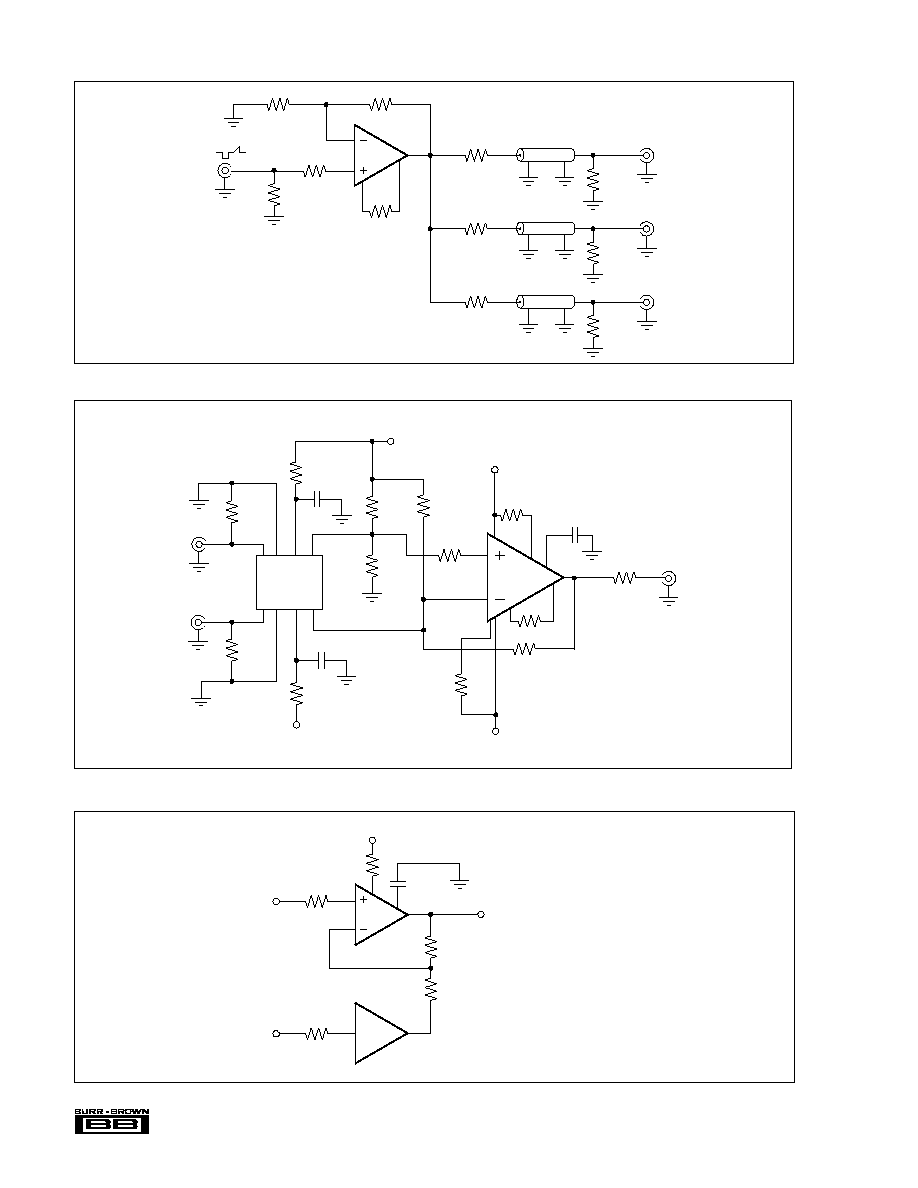
FIGURE 18. Video Distribution Amplifier.
FIGURE 19. Wideband Multiplier Output Amplifier.
FIGURE 20. Current-Feedback Amplifier with Two Equal and High Impedance Inputs.
R
2
/R
N
sets the closed-loop gain; C
OTA
sets the first
open-loop pole; R
2
|| R
N
sets the open-loop gain.
+G
CL
= 1 + -- = +2V/V
R
2
R
N
CFA
OB
≠5V
R
QC
630
R
IN
150
R
IN
150
V
IN
V
IN
3
8
R
N
180
R
2
180
9
1pF
C
OTA
V
OUT
= G
CL
(V
IN
- V
IN
) + V
IN
+
≠
≠
+
≠
330
75
OPA622
AP
330
75
V
OUT
75
75
V
OUT
75
75
V
OUT
75
9
3
4
13
8
R
OG
150
Bandwidth, (5Vp-p) = 150MHz (OPA622AP)
200MHz (OPA622AU)
High output current drive capability (6Vp-p
into 50
) allows three back-terminated 75
transmission lines to be simultaneously driven.
Video
Input
75
Transmission Line
150
X
2
X
1
+V W
1
Y
1
Y
2
≠V W
2
Wideband
Multiplier
50
50
100
100
100
100
100
150
10
100
330
50
10
V
IN2
V
IN1
1µF
1µF
+6V
4
3
6
5
8
13
9
10
11
12
+6V
1µF
V
OUT
≠6V
≠6V
OPA622