 | –≠–ª–µ–∫—Ç—Ä–æ–Ω–Ω—ã–π –∫–æ–º–ø–æ–Ω–µ–Ω—Ç: OPA640U | –°–∫–∞—á–∞—Ç—å:  PDF PDF  ZIP ZIP |

Æ
OPA640
1
FEATURES
q
UNITY-GAIN BANDWIDTH: 1.3GHz
q
UNITY-GAIN STABLE
q
LOW NOISE: 2.9nV/
Hz
q
LOW HARMONICS: ≠75dBc at 10MHz
q
HIGH COMMON MODE REJECTION: 85dB
q
HIGH SLEW RATE: 350V/
µ
s
OPA640
Wideband Voltage Feedback
OPERATIONAL AMPLIFIER
DESCRIPTION
The OPA640 is an extremely wideband operational
amplifier featuring low noise, high common-mode
rejection and high spurious free dynamic range.
The OPA640 is internally compensated for unity-gain
stability. This amplifier has a fully symmetrical differ-
ential input due to its "classical" operational amplifier
circuit architecture. This allows the OPA640 to be used
in all op amp applications requiring high speed and
precision.
Low noise, wide bandwidth, and high linearity make
this amplifier suitable for a variety of RF and video
applications.
Æ
International Airport Industrial Park ∑ Mailing Address: PO Box 11400, Tucson, AZ 85734 ∑ Street Address: 6730 S. Tucson Blvd., Tucson, AZ 85706 ∑ Tel: (520) 746-1111 ∑ Twx: 910-952-1111
Internet: http://www.burr-brown.com/ ∑ FAXLine: (800) 548-6133 (US/Canada Only) ∑ Cable: BBRCORP ∑ Telex: 066-6491 ∑ FAX: (520) 889-1510 ∑ Immediate Product Info: (800) 548-6132
OPA640
OPA640
APPLICATIONS
q
COMMUNICATIONS
q
MEDICAL IMAGING
q
TEST EQUIPMENT
q
CCD IMAGING
q
ADC/DAC GAIN AMPLIFIER
q
HIGH-RESOLUTION VIDEO
q
LOW NOISE PREAMPLIFIER
q
DIFFERENTIAL AMPLIFIER
q
ACTIVE FILTERS
Current
Mirror
Output
Stage
C
C
3
2
Non-Inverting
Input
Inverting
Input
7, 8
+V
S
4, 5
≠V
S
6
V
OUT
©
1993 Burr-Brown Corporation
PDS-1179D
Printed in U.S.A. March, 1998

2
OPA640
Æ
SPECIFICATIONS
ELECTRICAL
At T
A
= +25
∞
C, V
S
=
±
5V, R
L
= 100
, C
L
= 2pF, R
FB
= 402
and all four power supply pins are used, unless otherwise noted. R
FB
= 25
for a gain of +1.
OPA640P, U
OPA640UB
PARAMETER
CONDITIONS
MIN
TYP
MAX
MIN
TYP
MAX
UNITS
OFFSET VOLTAGE
Input Offset Voltage
±
2.0
±
5
1.0
±
2.0
mV
Average Drift,
±
10
±
6
µ
V/
∞
C
Power Supply Rejection (+V
S
)
V
S
=
±
4.5 to
±
5.5V
60
75
T
T
dB
(≠V
S
)
53
60
T
T
dB
INPUT BIAS CURRENT
(1)
Input Bias Current
V
CM
= 0V
15
25
T
T
µ
A
Over Specified Temperature
30
75
18
55
µ
A
Input Offset Current
V
CM
= 0V
0.3
2.0
T
1.0
µ
A
Over Specified Temperature
0.5
2.5
T
2.0
µ
A
NOISE
Input Voltage Noise Density
f = 100Hz
7.0
T
nV/
Hz
f = 10kHz
2.8
T
nV/
Hz
f = 1MHz
2.8
T
nV/
Hz
f = 1MHz to 500MHz
2.9
T
nV/
Hz
Voltage Noise, BW = 100Hz to 500MHz
65
T
µ
Vrms
Input Bias Current Noise Density
f = 0.1Hz to 20kHz
2.0
T
pA/
Hz
Noise Figure (NF)
R
S
= 1k
2.6
T
dB
R
S
= 50
10.9
T
dB
INPUT VOLTAGE RANGE
Common-Mode Input Range
±
2.5
±
2.85
T
T
V
Over Temperature
±
2.5
±
2.75
T
T
V
Common-Mode Rejection
V
CM
=
±
0.5V
70
85
80
88
dB
INPUT IMPEDANCE
Differential
15 || 1
T
k
|| pF
Common-Mode
2 || 1
T
M
|| pF
OPEN-LOOP GAIN, DC
Open-Loop Voltage Gain
V
O
=
±
2V, R
L
= 100
50
57
53
T
dB
Over Specified Temperature
V
O
=
±
2V, R
L
= 100
45
55
T
T
dB
FREQUENCY RESPONSE
Closed-Loop Bandwidth
Gain = +1V/V
1.3
T
GHz
Gain = +2V/V
280
T
MHz
Gain = +5V/V
65
T
MHz
Gain = +10V/V
31
T
MHz
Slew Rate
(2)
G = +1, 2V Step
350
T
V/
µ
s
At Minimum Specified Temperature
G = +1, 2V Step
285
T
V/
µ
s
Settling Time
0.01%
G = +1, 2V Step
22
T
ns
0.1%
G = +1, 2V Step
18
T
ns
1%
G = +1, 2V Step
4.5
T
ns
Spurious Free Dynamic Range
G = +1, f = 5MHz, V
O
= 2Vp-p
85
T
dBc
G = +1, f = 10MHz, V
O
= 2Vp-p
75
T
dBc
G = +1, f = 20MHz, V
O
= 2Vp-p
65
T
dBc
Gain Flatness to 0.1dB
G = +1 or +2
120
T
MHz
Differential Gain at 3.58MHz,
V
O
= 0V to 1.4V, R
L
= 150
0.07
T
%
G = +2V/V
Differential Phase at 3.58MHz,
V
O
= 0V to 1.4V, R
L
= 150
0.008
T
Degrees
G = +2V/V
OUTPUT
Voltage Output
No Load
Over Specified Temperature
±
2.6
±
3.0
T
T
V
Voltage Output
R
L
= 100
Over Specified Temperature
±
2.25
±
2.5
T
T
V
Current Output, +25
∞
C
±
40
±
52
T
T
mA
Over Specified Temperature
±
25
±
45
T
T
mA
Short Circuit Current
75
T
mA
Output Resistance
1MHz, G = +1V/V
0.2
T
POWER SUPPLY
Specified Operating Voltage
T
MIN
to T
MAX
±
5
T
V
Operating Voltage Range
T
MIN
to T
MAX
±
4.5
±
5.5
T
T
V
Quiescent Current
±
18
±
22
T
T
mA
Over Specified Temperature
±
19
±
24
T
T
mA
TEMPERATURE RANGE
Specification: P, U, UB
Ambient
≠40
+85
T
T
∞
C
Thermal Resistance
JA
, Junction to Ambient
∞
C/W
P
8-Pin DIP
100
T
∞
C/W
U, UB
8-Pin SO-8
125
T
∞
C/W
NOTE: (1) Slew rate is rate of change from 10% to 90% of output voltage step.
Æ
OPA640
3
The information provided herein is believed to be reliable; however, BURR-BROWN assumes no responsibility for inaccuracies or omissions. BURR-BROWN assumes
no responsibility for the use of this information, and all use of such information shall be entirely at the user's own risk. Prices and specifications are subject to change
without notice. No patent rights or licenses to any of the circuits described herein are implied or granted to any third party. BURR-BROWN does not authorize or warrant
any BURR-BROWN product for use in life support devices and/or systems.
ABSOLUTE MAXIMUM RATINGS
Power Supply ..............................................................................
±
5.5VDC
Internal Power Dissipation .................................. Thermal Considerations
Differential Input Voltage ..................................................................
±
1.2V
Input Voltage Range ............................................................................
±
V
S
Storage Temperature Range: P, U, UB ........................ ≠40
∞
C to +125
∞
C
Lead Temperature (soldering, 10s) .............................................. +300
∞
C
(soldering, SO-8 3s) ....................................... +260
∞
C
Junction Temperature (T
J
) ............................................................ +175
∞
C
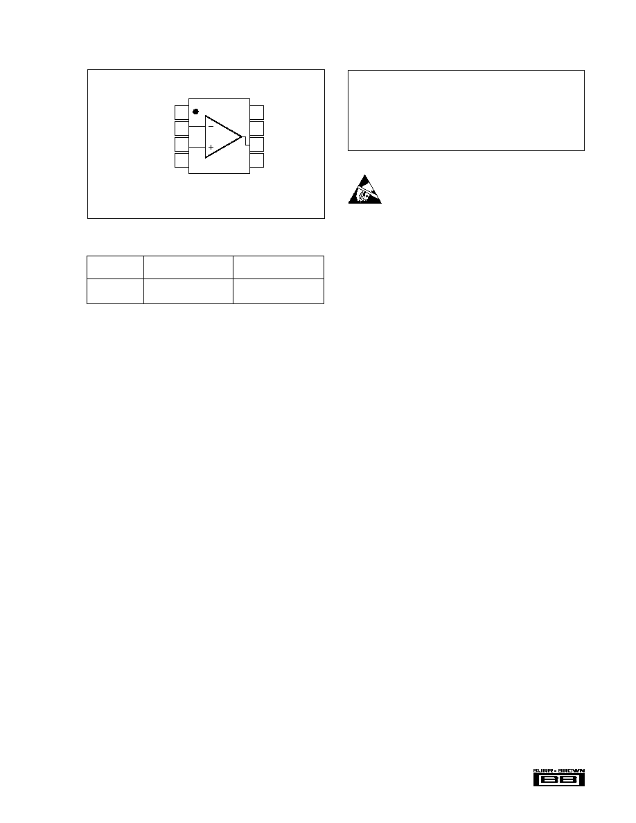
PIN CONFIGURATION
NOTE: (1) Making use of all four power supply pins is highly recommended,
although not required. Using these four pins, instead of just pins 4 and 7, will
lower the effective pin impedance and substantially lower distortion.
Top View
DIP/SO-8
ELECTROSTATIC
DISCHARGE SENSITIVITY
Electrostatic discharge can cause damage ranging from per-
formance degradation to complete device failure. Burr-
Brown Corporation recommends that all integrated circuits
be handled and stored using appropriate ESD protection
methods.
ESD damage can range from subtle performance degrada-
tion to complete device failure. Precision integrated circuits
may be more susceptible to damage because very small
parametric changes could cause the device not to meet
published specifications.
PACKAGE DRAWING
PRODUCT
PACKAGE
NUMBER
(1)
OPA640P
8-Pin Plastic DIP
006
OPA640U, UB
SO-8 Surface Mount
182
NOTE: (1) For detailed drawing and dimension table, please see end of data
sheet, or Appendix C of Burr-Brown IC Data Book. (2) The "B" grade of the
SO-8 and package will be marked with a "B" by pin 8.
PACKAGE/ORDERING INFORMATION
1
2
3
4
8
7
6
5
+V
S2
(1)
+V
S1
Output
≠V
S2
(1)
NC
Inverting Input
Non-Inverting Input
≠V
S1
4
OPA640
Æ
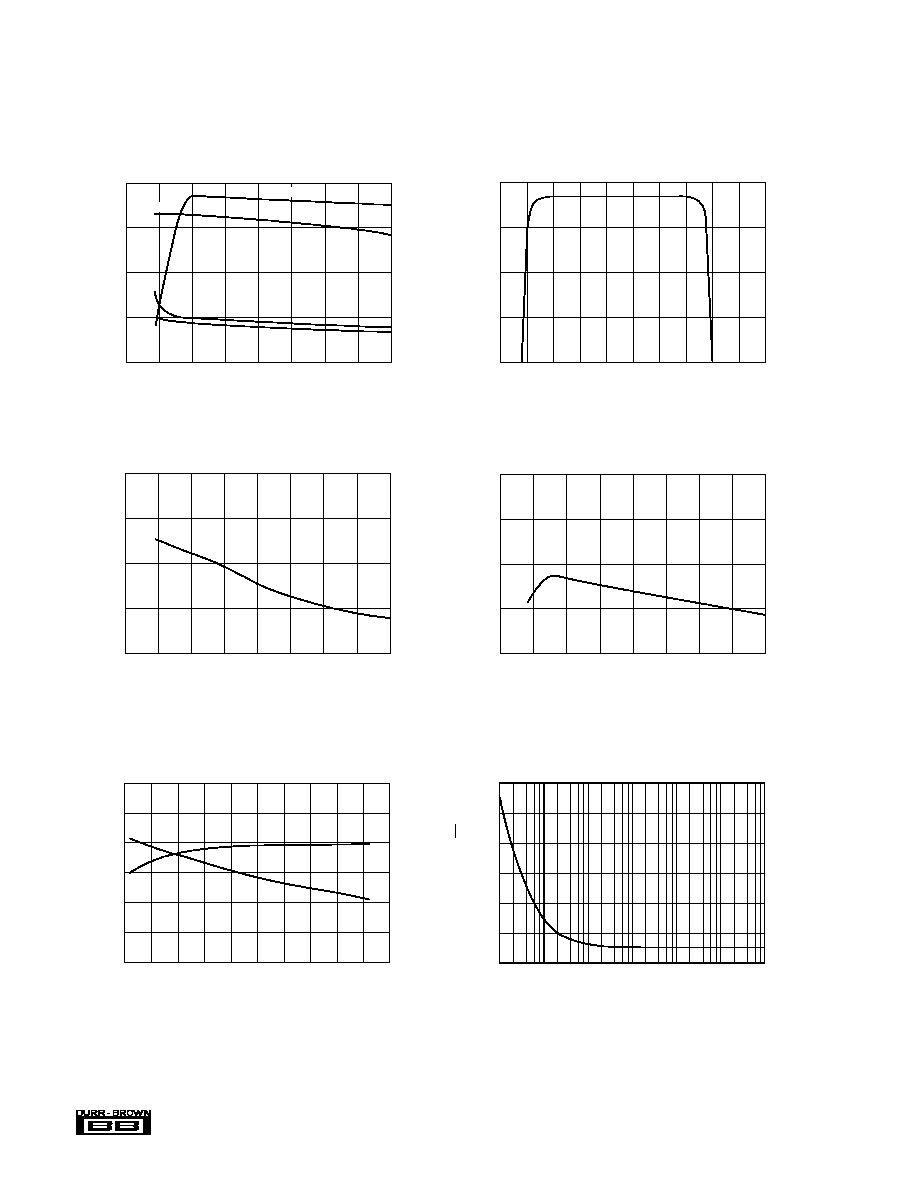
TYPICAL PERFORMANCE CURVES
T
A
= +25
∞
C, V
S
=
±
5V, R
L
= 100
, C
L
= 2pF, R
FB
= 402
and all four power supply pins are used, unless otherwise noted. R
FB
= 25
for a gain of +1.
90
80
70
60
50
≠75
Temperature (∞C)
A
OL
, PSR, CMR (dB)
A
OL
, PSR, AND CMR vs TEMPERATURE
≠50
≠25
0
25
50
75
100
125
≠PSR
A
OL
+PSR
CMR
90
85
80
75
70
≠5
Common-Mode Voltage (V)
Common-Mode Rejection (dB)
COMMON-MODE REJECTION
vs INPUT COMMON-MODE VOLTAGE
≠4
≠3
≠2
≠1
0
1
2
3
4
5
26
22
18
14
10
≠75
Ambient Temperature (∞C)
Input Bias Current (µA)
INPUT BIAS CURRENT vs TEMPERATURE
≠50
≠25
0
25
50
75
100
125
20
19
18
17
16
≠75
Ambient Temperature (∞C)
Supply Current (±mA)
SUPPLY CURRENT vs TEMPERATURE
≠50
≠25
0
25
50
75
100
125
70
60
50
40
≠60
Ambient Temperature (∞C)
Output Current (±mA)
OUTPUT CURRENT vs TEMPERATURE
≠40
≠20
0
20
40
60
80
100
120
140
≠I
O
+I
O
30
25
20
15
10
5
0
VOLTAGE NOISE vs FREQUENCY
Voltage Noise (nV/
Hz)
Frequency (Hz)
100
1k
10k
100k
1M
10M
10

Æ
OPA640
5
40
30
20
10
0
0
Capacitive Load (pF)
Isolation Resistance (
)
RECOMMENDED ISOLATION RESISTANCE
vs CAPACITIVE LOAD FOR G = +1
10
20
30
40
50
60
70
200
160
120
80
40
0
≠40
≠80
≠120
≠160
≠200
Time (5ns/Div)
Output Voltage (mV)
SMALL SIGNAL TRANSIENT RESPONSE
(G = +1, R
L
= 100
)
TYPICAL PERFORMANCE CURVES
(CONT)
T
A
= +25
∞
C, V
S
=
±
5V, R
L
= 100
, C
L
= 2pF, R
FB
= 402
and all four power supply pins are used, unless otherwise noted. R
FB
= 25
for a gain of +1.
2.0
1.6
1.2
0.8
0.4
0
≠0.4
≠0.8
≠1.2
≠1.6
≠1V
Time (5ns/Div)
Output Voltage (V)
LARGE SIGNAL TRANSIENT RESPONSE
(G = +1, R
L
= 100
)
A
V
= +5V/V CLOSED-LOOP
SMALL SIGNAL BANDWIDTH
Gain (dB)
Frequency (Hz)
1M
10M
100M
1G
17
14
11
8
5
2
≠1
≠4
0
≠45
≠90
Closed-Loop Phase (∞)
Closed-Loop
Phase
Bandwidth
= 68MHz
Gain
G = +1V/V CLOSED-LOOP
SMALL SIGNAL BANDWIDTH
Gain (dB)
Frequency (Hz)
10M
100M
1G
10G
9
6
3
0
≠3
≠6
≠9
≠12
≠15
≠18
≠21
0
≠45
≠90
≠135
≠180
≠225
≠270
Phase Margin (∞)
Gain
SO-8
Closed-Loop
Phase
DIP
Bandwidth
= 1.05GHz
SO-8
Bandwidth
= 1.45GHz
≠40∞C SO-8
Bandwidth
= 1.71GHz
G = +2V/V CLOSED-LOOP
SMALL SIGNAL BANDWIDTH
Gain (dB)
Frequency (Hz)
1M
10M
100M
1G
9
6
3
0
≠3
≠6
0
≠45
≠90
≠135
≠180
≠225
≠270
Phase Shift (∞)
Closed-Loop
Phase
SO-8
Bandwidth
= 286MHz
DIP
Bandwidth
= 262MHz
Gain

6
OPA640
Æ
TYPICAL PERFORMANCE CURVES
(CONT)
T
A
= +25
∞
C, V
S
=
±
5V, R
L
= 100
, C
L
= 2pF, R
FB
= 402
and all four power supply pins are used, unless otherwise noted. R
FB
= 25
for a gain of +1.
≠40
≠60
≠80
≠100
100k
Frequency (Hz)
Harmonic Distortion (dBc)
HARMONIC DISTORTION vs FREQUENCY
(G = +1, V
O
= 2Vp-p, R
L
= 100
)
1M
10M
100M
2f
O
3f
O
≠40
≠60
≠80
≠100
100k
Frequency (Hz)
Harmonic Distortion (dBc)
HARMONIC DISTORTION vs FREQUENCY
(G = ≠1, V
O
= 2Vp-p, R
L
= 100
)
1M
10M
100M
2f
O
3f
O
≠40
≠60
≠80
≠100
100k
Frequency (Hz)
Harmonic Distortion (dBc)
HARMONIC DISTORTION vs FREQUENCY
(G = +2, V
O
= 2Vp-p, R
L
= 100
)
1M
10M
100M
2f
O
3f
O
≠40
≠60
≠80
≠100
100k
Frequency (Hz)
Harmonic Distortion (dBc)
HARMONIC DISTORTION vs FREQUENCY
(G = +5, V
O
= 2Vp-p, R
L
= 100
)
1M
10M
100M
2f
O
3f
O
≠70
≠80
≠90
≠100
≠75
Ambient Temperature (∞C)
Harmonic Distortion (dBc)
HARMONIC DISTORTION vs TEMPERATURE
(G = +1, V
O
= 2Vp-p, R
L
= 100
, f
O
= 5MHz)
≠50
≠25
0
25
50
75
100
125
2f
O
3f
O
≠70
≠80
≠90
≠100
0
Output Swing (Vp-p)
Harmonic Distortion (dBc)
5MHz HARMONIC DISTORTION vs OUTPUT SWING
(G = +1, R
L
= 100
)
1.0
2.0
3.0
4.0
2f
O
3f
O

Æ
OPA640
7
TYPICAL PERFORMANCE CURVES
(CONT)
T
A
= +25
∞
C, V
S
=
±
5V, R
L
= 100
, C
L
= 2pF, R
FB
= 402
and all four power supply pins are used, unless otherwise noted. R
FB
= 25
for a gain of +1.
APPLICATIONS INFORMATION
DISCUSSION OF PERFORMANCE
The OPA640 provides a level of speed and precision not
previously attainable in monolithic form. Unlike current
feedback amplifiers, the OPA640's design uses a "Classi-
cal" operational amplifier architecture and can therefore be
used in all traditional operational amplifier applications.
While it is true that current feedback amplifiers can provide
wider bandwidth at higher gains, they offer some disadvan-
tages. The asymmetrical input characteristics of current
feedback amplifiers (i.e. one input is a low impedance)
prevents them from being used in a variety of applications.
In addition, unbalanced inputs make input bias current errors
difficult to correct. Cancelling offset errors (due to input bias
currents) through matching of inverting and non-inverting
input resistors is impossible because the input bias currents
are uncorrelated. Current noise is also asymmetrical and is
usually significantly higher on the inverting input. Perhaps
most important, settling time to 0.01% is often extremely
poor due to internal design tradeoffs. Many current feedback
designs exhibit settling times to 0.01% in excess of 10
microseconds even though 0.1% settling times are reason-
able. Such amplifiers are completely inadequate for fast
settling 12-bit applications.
The OPA640's "Classical" operational amplifier architec-
ture employs true differential and fully symmetrical inputs
to eliminate these troublesome problems. All traditional
circuit configurations and op amp theory apply to the
OPA640.
WIRING PRECAUTIONS
Maximizing the OPA640's capability requires some wiring
precautions and high-frequency layout techniques. Oscilla-
tion, ringing, poor bandwidth and settling, gain peaking, and
instability are typical problems plaguing all high-speed
amplifiers when they are improperly used. In general, all
printed circuit board conductors should be wide to provide
low resistance, low impedance signal paths. They should
also be as short as possible. The entire physical circuit
should be as small as practical. Stray capacitances should be
minimized, especially at high impedance nodes, such as the
amplifier's input terminals. Stray signal coupling from the
output or power supplies to the inputs should be minimized.
All circuit element leads should be no longer than 1/4 inch
(6mm) to minimize lead inductance, and low values of
resistance should be used. This will minimize time constants
formed with the circuit capacitances and will eliminate
stray, parasitic circuits.
Grounding is the most important application consideration
for the OPA640, as it is with all high-frequency circuits.
Oscillations at high frequencies can easily occur if good
grounding techniques are not used. A heavy ground plane
(2oz copper recommended) should connect all unused areas
on the component side. Good ground planes can reduce stray
signal pickup, provide a low resistance, low inductance
common return path for signal and power, and can conduct
heat from active circuit package pins into ambient air by
convection.
Supply bypassing is extremely critical and must always be
used, especially when driving high current loads. Both
power supply leads should be bypassed to ground as close as
possible to the amplifier pins. Tantalum capacitors (2.2
µ
F)
with very short leads are recommended. A parallel 0.01
µ
F
ceramic must also be added. Surface mount bypass capaci-
tors will produce excellent results due to their low lead
inductance. Additionally, suppression filters can be used to
isolate noisy supply lines. Properly bypassed and modula-
tion-free power supply lines allow full amplifier output and
optimum settling time performance.
≠65
≠75
≠85
≠95
0
Output Swing (Vp-p)
Harmonic Distortion (dBc)
10MHz HARMONIC DISTORTION vs OUTPUT SWING
(G = +1, R
L
= 100
)
1.0
2.0
3.0
4.0
2f
O
3f
O
8
OPA640
Æ
Points to Remember
1) Making use of all four power supply pins will lower the
effective power supply impedance seen by the input and
output stages. This will improve the AC performance in-
cluding lower distortion. The lowest distortion is achieved
when running separate traces to V
S1
and V
S2
. Power supply
bypassing with 0.01
µ
F and 2.2
µ
F surface mount capacitors
on the topside of the PC board is recommended. It is
essential to keep the 0.01
µ
F capacitor very close to the
power supply pins. Refer to the DEM-OPA64X data sheet
for the recommended layout and component placements.
2) Whenever possible, use surface mount. Don't use point-
to-point wiring as the increase in wiring inductance will be
detrimental to AC performance. However, if it must be used,
very short, direct signal paths are required. The input signal
ground return, the load ground return, and the power supply
common should all be connected to the same physical point
to eliminate ground loops, which can cause unwanted feed-
back.
3) Surface mount on backside of PC Board. Good compo-
nent selection is essential. Capacitors used in critical loca-
tions should be a low inductance type with a high quality
dielectric material. Likewise, diodes used in critical loca-
tions should be Schottky barrier types, such as HP5082-
2835 for fast recovery and minimum charge storage. Ordi-
nary diodes will not be suitable in RF circuits.
4) Whenever possible, solder the OPA640 directly into the
PC board without using a socket. Sockets add parasitic
capacitance and inductance, which can seriously degrade
AC performance or produce oscillations.
5) Use a small feedback resistor (usually 25
) in unity-gain
voltage follower applications for the best performance. For
gain configurations, resistors used in feedback networks
should have values of a few hundred ohms for best perfor-
mance. Shunt capacitance problems limit the acceptable
resistance range to about 1k
on the high end and to a value
that is within the amplifier's output drive limits on the low
end. Metal film and carbon resistors will be satisfactory, but
wirewound resistors (even "non-inductive" types) are abso-
lutely unacceptable in high-frequency circuits. Feedback
resistors should be placed directly between the output and
the inverting input on the backside of the PC board. This
placement allows for the shortest feedback path and the
highest bandwidth. Refer to the demonstration board layout
at the end of the data sheet. A longer feedback path than
this will decrease the realized bandwidth substantially.
6) Due to the extremely high bandwidth of the OPA640, the
SO-8 package is strongly recommended due its low parasitic
impedance. The parasitic impedance in the DIP and package
causes the OPA640 to experience about 5dB of gain peaking
in unity-gain configurations. This is compared with virtually
no gain peaking in the SO-8 package in unity-gain. The gain
peaking in the DIP package is minimized in gains of 2 or
greater, however. Surface mount components (chip resistors,
capacitors, etc.) have low lead inductance and are also
strongly recommended.
7) Avoid overloading the output. Remember that output
current must be provided by the amplifier to drive its own
feedback network as well as to drive its load. Lowest
distortion is achieved with high impedance loads.
8) Don't forget that these amplifiers use
±
5V supplies.
Although they will operate perfectly well with +5V and
≠5.2V, use of
±
15V supplies will destroy the part.
9) Standard commercial test equipment has not been de-
signed to test devices in the OPA640's speed range. Bench-
top op amp testers and ATE systems will require a special
test head to successfully test these amplifiers.
10) Terminate transmission line loads. Unterminated lines,
such as coaxial cable, can appear to the amplifier to be a
capacitive or inductive load. By terminating a transmission
line with its characteristic impedance, the amplifier's load
then appears purely resistive.
11) Plug-in prototype boards and wire-wrap boards will not
be satisfactory. A clean layout using RF techniques is
essential; there are no shortcuts.
OFFSET VOLTAGE ADJUSTMENT
If additional offset adjustment is needed, the circuit in
Figure 1 can be used without degrading offset drift with
temperature. Avoid external adjustment whenever possible
since extraneous noise, such as power supply noise, can be
inadvertently coupled into the amplifier's inverting input
terminal. Remember that additional offset errors can be
created by the amplifier's input bias currents. Whenever
possible, match the impedance seen by both inputs as is
shown with R
3.
This will reduce input bias current errors to
the amplifier's offset current.
FIGURE 1. Offset Voltage Trim.
NOTE: (1) R
3
is optional and can be used to cancel offset errors due to input
bias currents.
INPUT PROTECTION
Static damage has been well recognized for MOSFET de-
vices, but any semiconductor device deserves protection
from this potentially damaging source. The OPA640 incor-
porates on-chip ESD protection diodes as shown in Figure 2.
R
2
OPA640
R
3
= R
1
|| R
2
(1)
R
1
R
TRIM
47k
+V
CC
≠V
CC
20k
V
IN
or Ground
Output Trim Range +V
CC
to ≠V
CC
R
Trim
R
2
R
2
R
Trim
10µF
Æ
OPA640
9
This eliminates the need for the user to add external protec-
tion diodes, which can add capacitance and degrade AC
performance.
All pins on the OPA640 are internally protected from ESD
ESD Protection diodes internally
connected to all pins.
FIGURE 2. Internal ESD Protection.
External
Pin
+V
CC
≠V
CC
Internal
Circuitry
by means of a pair of back-to-back reverse-biased diodes to
either power supply as shown. These diodes will begin to
conduct when the input voltage exceeds either power supply
by about 0.7V. This situation can occur with loss of the
amplifier's power supplies while a signal source is still
present. The diodes can typically withstand a continuous
current of 30mA without destruction. To insure long term
reliability, however, diode current should be externally lim-
ited to 10mA or so whenever possible.
The OPA640 utilizes a fine geometry high speed process
that withstands 500V using Human Body Model and 100V
using the Machine Model. However, static damage can
cause subtle changes in amplifier input characteristics with-
out necessarily destroying the device. In precision opera-
tional amplifiers, this may cause a noticeable degradation of
offset voltage and drift. Therefore, static protection is strongly
recommended when handling the OPA640.
OUTPUT DRIVE CAPABILITY
The OPA640 has been optimized to drive 75
and 100
resistive loads. The device can drive 2Vp-p into a 75
load.
This high-output drive capability makes the OPA640 an
ideal choice for a wide range of RF, IF, and video applica-
tions. In many cases, additional buffer amplifiers are un-
needed.
Many demanding high-speed applications such as
ADC/DAC buffers require op amps with low wideband
output impedance. For example, low output impedance is
essential when driving the signal-dependent capacitances at
the inputs of flash A/D converters. As shown in Figure 3,
the OPA640 maintains very low closed-loop output imped-
ance over frequency. Closed-loop output impedance in-
creases with frequency since loop gain is decreasing with
frequency.
FIGURE 3. Closed-Loop Output Impedance vs Frequency.
THERMAL CONSIDERATIONS
The OPA640 does not require a heat sink for operation in
most environments. At extreme temperatures and under full
load conditions a heat sink may be necessary.
The internal power dissipation is given by the equation
P
D
= P
DQ
+ P
DL
, where P
DQ
is the quiescent power dissipation
and P
DL
is the power dissipation in the output stage due to the
load. (For
±
V
CC
=
±
5V, P
DQ
= 10V
x
22mA = 220mW, max).
For the case where the amplifier is driving a grounded load
(R
L
) with a DC voltage (
±
V
OUT
) the maximum value of P
DL
occurs at
±
V
OUT
=
±
V
CC
/2, and is equal to P
DL
,
max = (
±
V
CC
)
2
/4R
L
. Note that it is the voltage across the
output transistor, and not the load, that determines the power
dissipated in the output stage.
A short-circuit condition represents the maximum amount of
internal power dissipation that can be generated. The varia-
tion of output current with temperature is shown in Figure 4.
CAPACITIVE LOADS
FIGURE 4. Output Current vs. Temperature.
70
60
50
40
≠60
Ambient Temperature (∞C)
Output Current (±mA)
≠40
≠20
0
20
40
60
80
100
120
140
≠I
O
+I
O
100
10
1
0.1
0.01
0.001
10k
Frequency (Hz)
Output Impedance (
)
100k
1M
10M
100M
A
V
= +1V/V
10
OPA640
Æ
The OPA640's output stage has been optimized to drive low
resistive loads. Capacitive loads, however, will decrease the
amplifier's phase margin which may cause high frequency
peaking or oscillations. Capacitive loads greater than 2pF
should be buffered by connecting a small resistance, usually
5
to 25
, in series with the output as shown in Figure 5.
This is particularly important when driving high capacitance
loads such as flash A/D converters. Increasing the gain from
+1 will improve the capacitive load drive due to increased
phase margin.
In general, capacitive loads should be minimized for opti-
the phase margin and avoid peaking by keeping the break
frequency of this zero sufficiently high. When high closed-
loop gains are required, a three-resistor attenuator (tee net-
work) is recommended to avoid using large value resistors
with large time constants.
SETTLING TIME
Settling time is defined as the total time required, from the
input signal step, for the output to settle to within the
specified error band around the final value. This error band
is expressed as a percentage of the value of the output
transition, a 2V step. Thus, settling time to 0.01% requires
an error band of
±
200
µ
V centered around the final value of
2V.
Settling time, specified in an inverting gain of one, occurs in
only 15ns to 0.01% for a 2V step, making the OPA640 one
of the fastest settling monolithic amplifiers commercially
available. Settling time increases with closed-loop gain and
output voltage change as described in the Typical Perform-
ance Curves. Preserving settling time requires critical atten-
tion to the details as mentioned under "Wiring Precautions."
The amplifier also recovers quickly from input overloads.
Overload recovery time to linear operation from a 50%
overload is typically only 35ns.
In practice, settling time measurements on the OPA640
prove to be very difficult to perform. Accurate measurement
is next to impossible in all but the very best equipped labs.
Among other things, a fast flat-top generator and high speed
oscilloscope are needed. Unfortunately, fast flat-top genera-
tors, which settle to 0.01% in sufficient time, are scarce and
expensive. Fast oscilloscopes, however, are more commonly
available. For best results a sampling oscilloscope is recom-
mended. Sampling scopes typically have bandwidths that
are greater than 1GHz and very low capacitance inputs.
They also exhibit faster settling times in response to signals
that would tend to overload a real-time oscilloscope.
DIFFERENTIAL GAIN AND PHASE
Differential Gain (DG) and Differential Phase (DP) are
among the more important specifications for video applica-
tions. DG is defined as the percent change in closed-loop
gain over a specified change in output voltage level. DP is
defined as the change in degrees of the closed-loop phase
over the same output voltage change. Both DG and DP are
specified at the NTSC sub-carrier frequency of 3.58MHz.
DG and DP increase with closed-loop gain and output
voltage transition as shown in the Typical Performance
Curves. All measurements were performed using a Tektronix
model VM700 Video Measurement Set.
FIGURE 5. Driving Capacitive Loads.
OPA640
C
L
R
L
R
S
(R
S
typically 5
to 25
)
mum high frequency performance. Coax lines can be driven
if the cable is properly terminated. The capacitance of coax
cable (29pF/foot for RG-58) will not load the amplifier
when the coaxial cable or transmission line is terminated in
its characteristic impedance.
COMPENSATION
The OPA640 is internally compensated and is stable in unity
gain with a phase margin of approximately 60
∞
. However,
the unity gain buffer is the most demanding circuit configu-
ration for loop stability and oscillations are most likely to
occur in this gain. If possible, use the device in a noise gain
of two or greater to improve phase margin and reduce the
susceptibility to oscillation. (Note that, from a stability
standpoint, an inverting gain of ≠1V/V is equivalent to a
noise gain of 2.) Gain and phase response for other gains are
shown in the Typical Performance Curves.
The high-frequency response of the OPA640 in a good
layout is very flat with frequency. However, some circuit
configurations such as those where large feedback resis-
tances are used, can produce high-frequency gain peaking.
This peaking can be minimized by connecting a small
capacitor in parallel with the feedback resistor. This capaci-
tor compensates for the closed-loop, high frequency, transfer
function zero that results from the time constant formed by
the input capacitance of the amplifier (typically 2pF after PC
board mounting), and the input and feedback resistors. The
selected compensation capacitor may be a trimmer, a fixed
capacitor, or a planned PC board capacitance. The capaci-
tance value is strongly dependent on circuit layout and
closed-loop gain. Using small resistor values will preserve
Æ
OPA640
11
DISTORTION
The OPA640's Harmonic Distortion characteristics vs fre-
quency and power output are shown in the Typical Perfor-
mance Curves. Distortion can be further improved by in-
creasing the load resistance. Refer to Figure 6. Remember to
include the contribution of the feedback resistance when
calculating the effective load resistance seen by the ampli-
fier.
FIGURE 6. 5MHz Harmonic Distortion vs Load Resistance.
The third-order intercept point is an important parameter for
many RF amplifier applications. Figure 7 shows the
OPA640's single tone, third-order intercept vs frequency.
This curve is particularly useful for determining the magni-
tude of the third harmonic as a function of frequency, load
resistance, and gain. For example, assume that the applica-
tion requires the OPA640 to operate in a gain of +1V/V and
drive 2Vp-p into 50
at a frequency of 10MHz. Referring to
Figure 11 we find that the intercept point is +47dBm. The
magnitude of the third harmonic can now be easily calcu-
lated from the expression:
Third Harmonic (dBc) = 2(OPI
3
P ≠ P
O
)
where OPI
3
P = third-order intercept, dBm
P
O
= output level, dBm
For this case OPI
3
P = 47dBm, P
O
= 47dBm, and the third
Harmonic = 2(47 ≠ 10) = 74dB below the fundamental tone.
The OPA640's low distortion makes the device an excellent
choice for a variety of RF signal processing applications.
The value for the two-tone, third-order intercept is typically
8dB lower than the single tone value.
FIGURE 7. Single-Tone , 3rd-Order Intercept Point vs Fre-
quency.
NOTE: Feedback Resistance used was 402
.
NOISE FIGURE
The OPA640 voltage and current noise spectral densities are
specified in the Typical Performance Curves. For RF appli-
cations, however, Noise Figure (NF) is often the preferred
noise specification since it allows system noise performance
to be more easily calculated. The OPA640's Noise Figure vs
Source Resistance is shown in Figure 8.
FIGURE 8. Noise Figure vs Source Resistance.
≠70
≠80
≠90
≠100
10
Load Resistance (
)
Harmonic Distortion (dBc)
20
50
100
200
500
1k
2f
O
3f
O
Noise Figure (dB)
Source Resistance (
)
10
100
1k
10k
25
20
15
10
5
0
100k
NF = 10 LOG 1 +
e
n
2
+ (I
n
R
S
)
2
4KTR
S
+60
+50
+40
+30
+20
Frequency (Hz)
10M
100M
1M
Third-Order Intercept Point (dBm)

12
OPA640
Æ
DEMONSTRATION BOARDS
Demonstration boards to speed prototyping are available.
Refer to the DEM-OPA64x data sheet for details.
FIGURE 10. ADC Input Buffer Amplifier (G = +2V/V).
Input
499
499
High Speed
ADC
499
OPA640
Input
R
S
NOTE: (1) Select J
1
, J
2
and R
1
,
R
2
to set input stage current for
optimum performance.
Input Bias Current: 1pA
OPA640
V
OUT
+5V
(≠)
(+)
D
S
J
1
(1)
D
S
2N5911
≠5V
2
3
7
6
4
J
2
(1)
R
2
(1)
2k
R
1
(1)
2k
FIGURE 11. Unity Gain Difference Amplifier.
OPA640
402
402
Single-
Ended
Output
402
402
Differential
Input
APPLICATIONS
FIGURE 9. Low Noise, Wideband FET Input Op Amp.
SPICE MODELS
Computer simulation using SPICE is often useful when
analyzing the performance of analog circuits and systems.
This is particularly true for Video and RF amplifier circuits
where parasitic capacitance and inductance can have a major
effect on circuit performance. SPICE models are available
for the OPA640. Contact Burr-Brown Applications Depart-
ment to receive a spice diskette.

Æ
OPA640
13
FIGURE 12. Video Gain Amplifier.
OPA640
Differential
Input
50
or 75
Transmission Line
50
or
75
402
OPA640
402
50
or
75
R
F
402
R
F
50
or 75
50
or
75
50
or
75
Differential
Output
R
G
50
or 75
Transmission Line
50
or 75
Differential Voltage Gain = 2V/V = 1 + 2R
F
/R
G
FIGURE 13. Differential Line Driver for 50
or 75
Systems.
FIGURE 14. Wideband, Fast-Settling Instrumentation Amplifier.
Differential Voltage Gain = 2V/V = 1 + 2R
F
/R
G
OPA640
V
OUT
402
402
Video
Input
75
75
75
Transmission Line
75
OPA640
806
OPA640
402
R
F
402
R
G
402
R
F
249
OPA640
402
402