 | ÐлекÑÑоннÑй компоненÑ: OPA660AP | СкаÑаÑÑ:  PDF PDF  ZIP ZIP |
Äîêóìåíòàöèÿ è îïèñàíèÿ www.docs.chipfind.ru

© 1990 Burr-Brown Corporation
PDS-1072F
Printed in U.S.A. April, 1995
Wide Bandwidth
OPERATIONAL TRANSCONDUCTANCE
AMPLIFIER AND BUFFER
APPLICATIONS
q
BASE LINE RESTORE CIRCUITS
q
VIDEO/BROADCAST EQUIPMENT
q
COMMUNICATIONS EQUIPMENT
q
HIGH-SPEED DATA ACQUISITION
q
WIDEBAND LED DRIVER
q
AGC-MULTIPLIER
q
NS-PULSE INTEGRATOR
q
CONTROL LOOP AMPLIFIER
q
400MHz DIFFERENTIAL INPUT
AMPLIFIER
FEATURES
q
WIDE BANDWIDTH: 850MHz
q
HIGH SLEW RATE: 3000V/
µ
s
q
LOW DIFFERENTIAL GAIN/PHASE
ERROR: 0.06%/0.02
°
q
VERSATILE CIRCUIT FUNCTION
q
EXTERNAL I
Q
-CONTROL
DESCRIPTION
The OPA660 is a versatile monolithic component
designed for wide-bandwidth systems including high
performance video, RF and IF circuitry. It includes a
wideband, bipolar integrated voltage-controlled cur-
rent source and voltage buffer amplifier.
The voltage-controlled current source or Operational
Transconductance Amplifier (OTA) can be viewed as
an "ideal transistor." Like a transistor, it has three
terminals--a high-impedance input (base), a low-
impedance input/output (emitter), and the current
output (collector). The OTA, however, is self-biased
and bipolar. The output current is zero-for-zero dif-
ferential input voltage. AC inputs centered about zero
produce an output current which is bipolar and cen-
tered about zero. The transconductance of the OTA
can be adjusted with an external resistor, allowing
bandwidth, quiescent current and gain trade-offs to
be optimized.
The open-loop buffer amplifier provides 850MHz
bandwidth and 3000V/
µ
s slew rate. Used as a basic
building block, the OPA660 simplifies the design of
AGC amplifiers, LED driver circuits for Fiber Optic
Transmission, integrators for fast pulses, fast control
loop amplifiers, and control amplifiers for capacitive
sensors and active filters.
The OPA660 is packaged in SO-8 surface-mount,
and 8-pin plastic DIP, specified from 40
°
C to +85
°
C.
OTA
B
E
C
3
8
2
5
6
+1
100
V
I
200
R
P
82
V
O
R
1
C
P
6.4pF
I
Q
= 20mA
R
5
100
G = 1 + = 3
R
3
2R
5
X
E
R
3
390
15
10
5
0
5
10
15
20
25
1M
10M
100M
1G
Frequency (Hz)
Output Voltage (dB)
OPA660 DIRECT-FEEDBACK FREQUENCY RESPONSE
20
30
100k
0.2Vp-p
5Vp-p
2.8Vp-p
1.4Vp-p
0.6Vp-p
OPA660
OPA660
OPA660
®
International Airport Industrial Park · Mailing Address: PO Box 11400, Tucson, AZ 85734 · Street Address: 6730 S. Tucson Blvd., Tucson, AZ 85706 · Tel: (520) 746-1111 · Twx: 910-952-1111
Internet: http://www.burr-brown.com/ · FAXLine: (800) 548-6133 (US/Canada Only) · Cable: BBRCORP · Telex: 066-6491 · FAX: (520) 889-1510 · Immediate Product Info: (800) 548-6132

2
®
OPA660
SPECIFICATIONS
Typical at I
Q
= 20mA, V
S
=
±
5V, T
A
= +25
°
C, and R
L
= 500
,
unless otherwise specified.
OPA660AP, AU
PARAMETER
CONDITIONS
MIN
TYP
MAX
UNITS
OTA TRANSCONDUCTANCE
Transconductance
V
C
= 0V
75
125
200
mA/V
OTA INPUT OFFSET VOLTAGE
V
B
= 0
Initial
+10
±
30
mV
vs Temperature
50
µ
V/
°
C
vs Supply (tracking)
V
S
=
±
4.5V to
±
5.5V
55
60
dB
vs Supply (non-tracking)
V+ = 4.5V to 5.5V
40
45
dB
vs Supply (non-tracking)
V = 4.5V to 5.5V
40
48
dB
OTA B-INPUT BIAS CURRENT
Initial
2.1
±
5
µ
A
vs Temperature
5
nA/
°
C
vs Supply (tracking)
V
S
=
±
4.5V to
±
5.5V
±
750
nA/V
vs Supply (non-tracking)
V+ = 4.5V to 5.5V
±
1500
nA/V
vs Supply (non-tracking)
V = 4.5V to 5.5V
±
500
nA/V
OTA OUTPUT BIAS CURRENT
Output Bias Current
V
B
= 0, V
C
= 0V
±
10
±
20
µ
A
vs Temperature
500
nA/
°
C
vs Supply (tracking)
V
S
=
±
4.5V to
±
5.5V
±
10
±
25
µ
A/V
vs Supply (non-tracking)
V+ = 4.5V to 5.5V
±
10
±
25
µ
A/V
vs Supply (non-tracking)
V = 4.5V to 5.5V
±
10
±
25
µ
A/V
OTA OUTPUT
Output Current
±
10
±
15
mA
Output Voltage Compliance
I
C
=
±
1mA
±
4.0
±
4.7
V
Output Impedance
25k || 4.2
|| pF
Open-Loop Gain
f = 1kHz
70
dB
BUFFER OFFSET VOLTAGE
Initial
+7
±
30
mV
vs Temperature
50
µ
V/
°
C
vs Supply (tracking)
V
S
=
±
4.5V to
±
5.5V
55
60
dB
vs Supply (non-tracking)
V+ = 4.5V to 5.5V
40
45
dB
vs Supply (non-tracking)
V = 4.5V to 5.5V
40
48
dB
BUFFER INPUT BIAS CURRENT
Initial
2.1
±
5
µ
A
vs Temperature
5
nA/
°
C
vs Supply (tracking)
V
S
=
±
4.5V to
±
5.5V
±
750
nA/V
vs Supply (non-tracking)
V+ = 4.5V to 5.5V
±
1500
nA/V
vs Supply (non-tracking)
V = 4.5V to 5.5V
±
500
nA/V
BUFFER and OTA INPUT IMPEDANCE
Input Impedance
1.0 || 2.1
M
|| pF
BUFFER INPUT NOISE
Voltage Noise Density, f = 100kHz
4
nV/
Hz
BUFFER DYNAMIC RESPONSE
Small Signal Bandwidth
V
O
=
±
100mV
850
MHz
Full Power Bandwidth
V
O
=
±
1.4V
800
MHz
V
O
=
±
2.5V
570
MHz
Differential Gain Error
3.58MHz, at 0.7V
0.06
%
Differential Phase Error
3.58MHz, at 0.7V
0.02
Degrees
Harmonic Distortion, 2nd Harmonic
f = 10MHz, V
O
= 0.5Vp-p
68
dBc
Slew Rate
5V Step
3000
V/
µ
s
Settling Time 0.1%
2V Step
25
ns
Rise Time (10% to 90%)
V
O
= 100mVp-p
1
ns
5V Step
1.5
ns
Group Delay Time
250
ps
BUFFER RATED OUTPUT
Voltage Output
I
O
=
±
1mA
±
3.7
±
4.2
V
Current Output
±
10
±
15
mA
Gain
R
L
= 500
0.96
0.975
V/V
R
L
= 5k
0.99
V/V
Output Impedance
7 || 2
|| pF
POWER SUPPLY
Voltage, Rated
±
5
V
Derated Performance
±
4.5
±
5.5
V
Quiescent Current (Programmable, Useful Range)
±
3 to
±
26
mA
3
®
OPA660
The information provided herein is believed to be reliable; however, BURR-BROWN assumes no responsibility for inaccuracies or omissions. BURR-BROWN assumes
no responsibility for the use of this information, and all use of such information shall be entirely at the user's own risk. Prices and specifications are subject to change
without notice. No patent rights or licenses to any of the circuits described herein are implied or granted to any third party. BURR-BROWN does not authorize or warrant
any BURR-BROWN product for use in life support devices and/or systems.
ABSOLUTE MAXIMUM RATINGS
Power Supply Voltage .........................................................................
±
6V
Input Voltage
(1)
........................................................................
±
V
S
±
0.7V
Operating Temperature ................................................... 40
°
C to +85
°
C
Storage Temperature ..................................................... 40
°
C to +125
°
C
Junction Temperature .................................................................... +175
°
C
Lead Temperature (soldering, 10s) ............................................... +300
°
C
NOTE: (1) Inputs are internally diode-clamped to
±
V
S
.
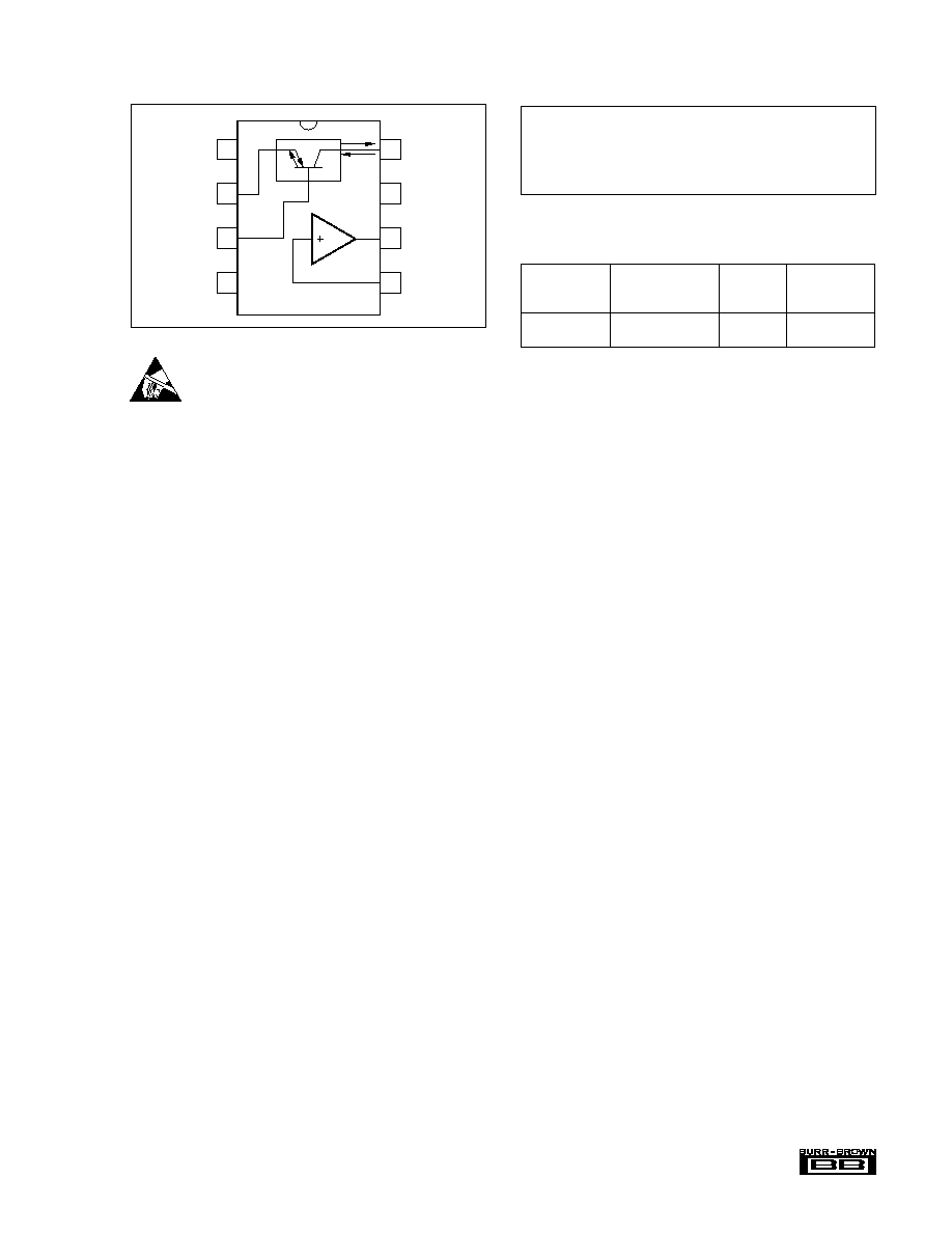
Top View
DIP/SO-8
I Adjust
E
B
V = 5V
C
V+ = +5V
Out
In
1
2
3
4
8
7
6
5
Q
1
ELECTROSTATIC
DISCHARGE SENSITIVITY
This integrated circuit can be damaged by ESD. Burr-Brown
recommends that all integrated circuits be handled with
appropriate precautions. Failure to observe proper handling
and installation procedures can cause damage.
ESD damage can range from subtle performance degradation
to complete device failure. Precision integrated circuits may
be more susceptible to damage because very small parametric
changes could cause the device not to meet its published
specifications.
PIN CONFIGURATION
PACKAGE
DRAWING
TEMPERATURE
PRODUCT
PACKAGE
NUMBER
(1)
RANGE
OPA660AP
8-Pin Plastic DIP
006
25
°
C to +85
°
C
OPA660AU
SO-8 Surface-Mount
182
25
°
C to +85
°
C
NOTE: (1) For detailed drawing and dimension table, please see end of data
sheet, or Appendix C of Burr-Brown IC Data Book.
PACKAGE/ORDERING INFORMATION
4
®
OPA660
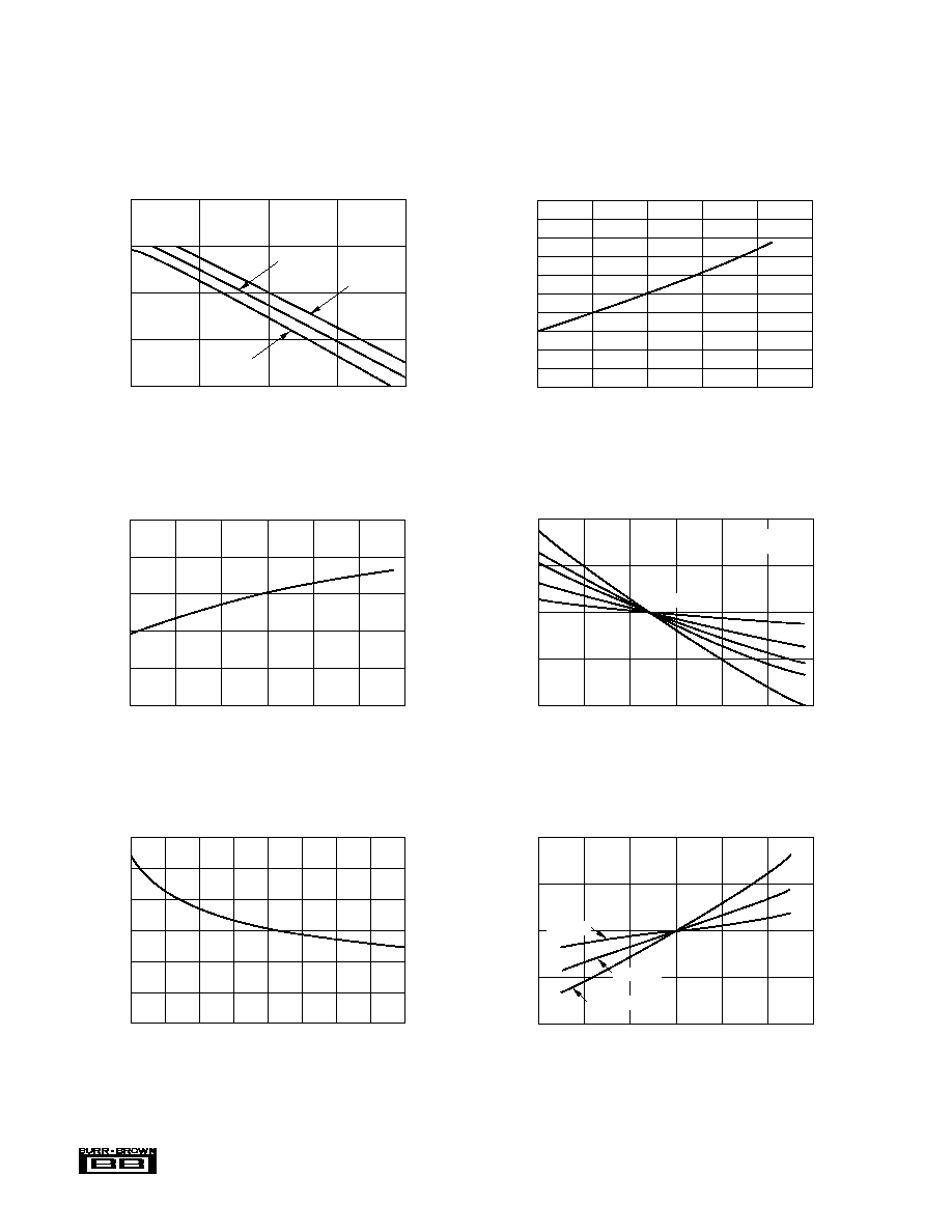
OTA TRANSFER CHARACTERISTICS
10
5
0
5
60
40
20
0
20
40
60
OTA Input Voltage (mV)
OTA Output Current (mA)
I
Q
= 20mA
I
Q
= 5mA
I
Q
= 10mA
10
OTA C-OUTPUT RESISTANCE
vs TOTAL QUIESCENT CURRENT (I
Q
)
4
Total Quiescent Current -- I
Q
(mA)
OTA Output Resistance (k )
6
8
10
12
14
16
18
20
60
50
40
30
20
10
0
OTA C-OUTPUT BIAS CURRENT vs TEMPERATURE
20
0
20
40
60
80
100
Temperature (°C)
OTA C-Output Bias Current (µA)
Trim Point
5 Representative
Units
40
20
40
100
Temperature (°C)
0.0
1.0
2.0
3.0
4.0
Input Bias Current (µA)
BUFFER AND OTA B-INPUT BIAS CURRENT
vs TEMPERATURE
80
0
20
60
5.0
TOTAL QUIESCENT CURRENT vs TEMPERATURE
25
25
100
Temperature (°C)
1.5
1.4
1.3
1.2
1.1
1.0
0.9
0.8
0.7
0.6
Total Quiescent Current (Normalized)
0
50
75
0.5
TYPICAL PERFORMANCE CURVES
I
Q
= 20mA, T
A
= +25
°
C, and V
S
=
±
5V unless otherwise noted.
100
1.0k
10k
R -- Resistor Value ( )
Q
100
30
10
3.0
Total Quiescent Current (mA)
TOTAL QUIESCENT CURRENT vs RQ
300
3.0k
1.0
Nominal
Device
Low I
Q
Device
High I
Q
Device
5
®
OPA660
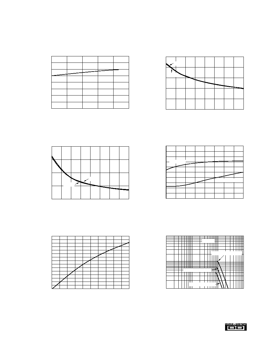
OTA TRANSCONDUCTANCE vs FREQUENCY
1M
10M
100M
1G
1000
100
OTA Transconductance (mA/V)
Frequency (Hz)
I
Q
= 20mA 106mA/V
I
Q
= 10mA 66mA/V
I
Q
= 5mA 40mA/V
R
L
= 50
10
BUFFER SLEW RATE
vs TOTAL QUIESCENT CURRENT (I
Q
)
4
Total Quiescent Current--I
Q
(mA)
4000
3800
3600
3400
3200
3000
2800
2600
2400
2200
Slew Rate (V/µs)
6
8
10
12
14
16
18
20
Rising Edge
Falling Edge
2000
BUFFER OUTPUT AND OTA E-OUTPUT RESISTANCE
vs TOTAL QUIESCENT CURRENT (I
Q
)
Total Quiescent Current--I
Q
(mA)
Buffer Output and OTA E-Output Resistance (
)
4
6
8
10
12
14
16
18
20
40
30
20
10
0
R
OUTBUF
R
OUTOTA
BUFFER AND OTA B-INPUT RESISTANCE
vs TOTAL QUIESCENT CURRENT (I
Q
)
4
Total Quiescent Current -- I (mA)
Buffer and OTA B-Input Resistance (M
)
6
8
10
12
14
16
18
20
Q
4
3
2
1
0
1
R
INOTA
R
INBUF
BUFFER AND OTA B-INPUT OFFSET VOLTAGE
vs TEMPERATURE
25
Temperature (°C)
20
15
10
5
0
5
10
15
Offset Voltage (mV)
0
25
50
75
100
20
TYPICAL PERFORMANCE CURVES
(CONT)
I
Q
= 20mA, T
A
= +25
°
C, and V
S
=
±
5V unless otherwise noted.
OTA TRANSCONDUCTANCE
vs TOTAL QUIESCENT CURRENT (I
Q
)
0
Total Quiescent Current--I
Q
(mA)
150
100
50
OTA Transconductance (mA/V)
4
6
8
10
12
16
18
20
0
2
14
6
®
OPA660
TRANSCONDUCTANCE vs INPUT VOLTAGE
160
120
80
40
0
40
30
20
10
0
10
20
30
40
R
Q
= 250
R
Q
= 500
R
Q
= 1k
R
Q
= 2k
Input Voltage (mV)
BUFFER MAX OUTPUT VOLTAGE vs FREQUENCY
10
0
Buffer Output Voltage (Vp-p)
1M
10M
100M
1G
Frequency (Hz)
0.1
15
10
5
0
5
10
15
20
25
1M
10M
100M
1G
Frequency (Hz)
Output Voltage (dB)
0.2Vp-p
0.6Vp-p
1.4Vp-p
3dB Point
I
Q
= 20mA R
IN
= 160
R
L
= 100
20
BUFFER FREQUENCY RESPONSE
dB
2.8Vp-p
200k
BUFFER VOLTAGE NOISE SPECTRAL DENSITY
100
10
100
1k
10k
100k
1M
10M
100M
Frequency (Hz)
Voltage Noise (nV/ Hz)
1
TYPICAL PERFORMANCE CURVES
(CONT)
I
Q
= 20mA, T
A
= +25
°
C, and V
S
=
±
5V unless otherwise noted.
Transconductance (mA/V)
OTA PULSE RESPONSE
Output Voltage = 5Vp-p
2.5V
+2.5V
0V
V
O
(V)
OTA PULSE RESPONSE
Input Voltage = 1.25Vp-p, t
R
= t
F
= 1ns, Gain = 4
0.625V
+0.625V
0V
V
O
(V)
7
®
OPA660
BUFFER DIFFERENTIAL PHASE ERROR
vs TOTAL QUIESCENT CURRENT (I
Q
)
4
Total Quiescent Current--I
Q
(mA)
0.10
0.09
0.08
0.07
0.06
0.05
0.04
0.03
0.02
0.01
Differential Phase Error (Degrees)
6
8
10
12
14
16
18
20
R
L
= 500
V
O
= 0.7Vp-p
f = 3.58MHz
0
BUFFER DIFFERENTIAL GAIN ERROR
vs TOTAL QUIESCENT CURRENT (I
Q
)
4
Total Quiescent Current --I
Q
(mA)
0.25
0.20
0.15
0.10
0.05
Differential Gain Error (%)
6
8
10
12
14
16
18
20
R
L
= 500
V
O
= 0.7Vp-p
f = 3.58MHz
0
5
6
+1
R
IN
= 50
Network
Analyzer
50
R
6
50
160
50
50
50
R
L
= R
6
+ R
7
||R
IN
= 100
V
I
V
O
R
7
TYPICAL PERFORMANCE CURVES
(CONT)
I
Q
= 20mA, T
A
= +25
°
C, and V
S
=
±
5V unless otherwise noted.
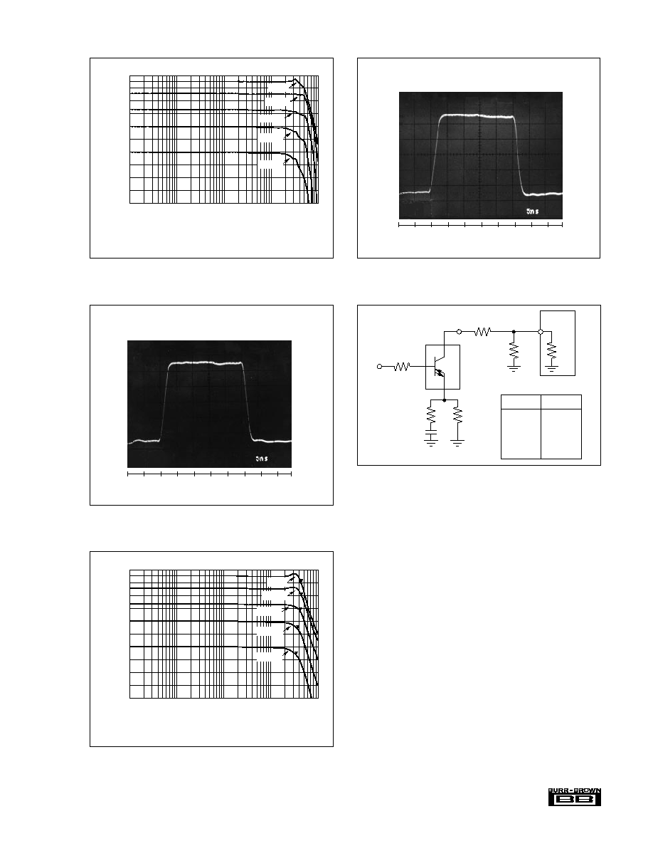
Test Circuit Buffer Pulse and Frequency Response
(HDTV Signal Pulse) t
R
= t
F
= 10ns, V
O
= 5Vp-p
t
R
= t
F
= 3ns, V
O
= 0.2Vp-p
V
O
(V)
BUFFER LARGE SIGNAL PULSE RESPONSE
V
O
(V)
BUFFER LARGE SIGNAL PULSE RESPONSE
t
R
= t
F
= 3ns, V
O
= 5Vp-p
8
®
OPA660
E
(2)
C
(8)
B
(3)
V
(6)
O
V
(5)
I
Bias
Circuitry
+V
CC
= +5V
BUFFER
OTA
100
50k
R (ext.)
Q
V
CC
= 5V
I Adj.
(1)
Q
(7)
(4)
HARMONIC DISTORTION vs FREQUENCY
30
40
50
60
70
10M
20M
40M
60M
100M
Frequency (Hz)
Harmonic Distortion (dBc)
R
L
= 500
I
Q
= 20mA
3f
2Vp-p
3f
0.5Vp-p
2f
2Vp-p
2f
0.5Vp-p
Measurement Limit
80
HARMONIC DISTORTION vs FREQUENCY
30
40
50
60
70
10M
20M
40M
60M
100M
2f
3f
Measurement Limit
Frequency (Hz)
Harmonic Distortion (dBc)
R
L
= 150
V
O
= 0.5Vp-p
I
Q
= 20mA
80
TYPICAL PERFORMANCE CURVES
(CONT)
I
Q
= 20mA, T
A
= +25
°
C, and V
S
=
±
5V unless otherwise noted.
APPLICATIONS INFORMATION
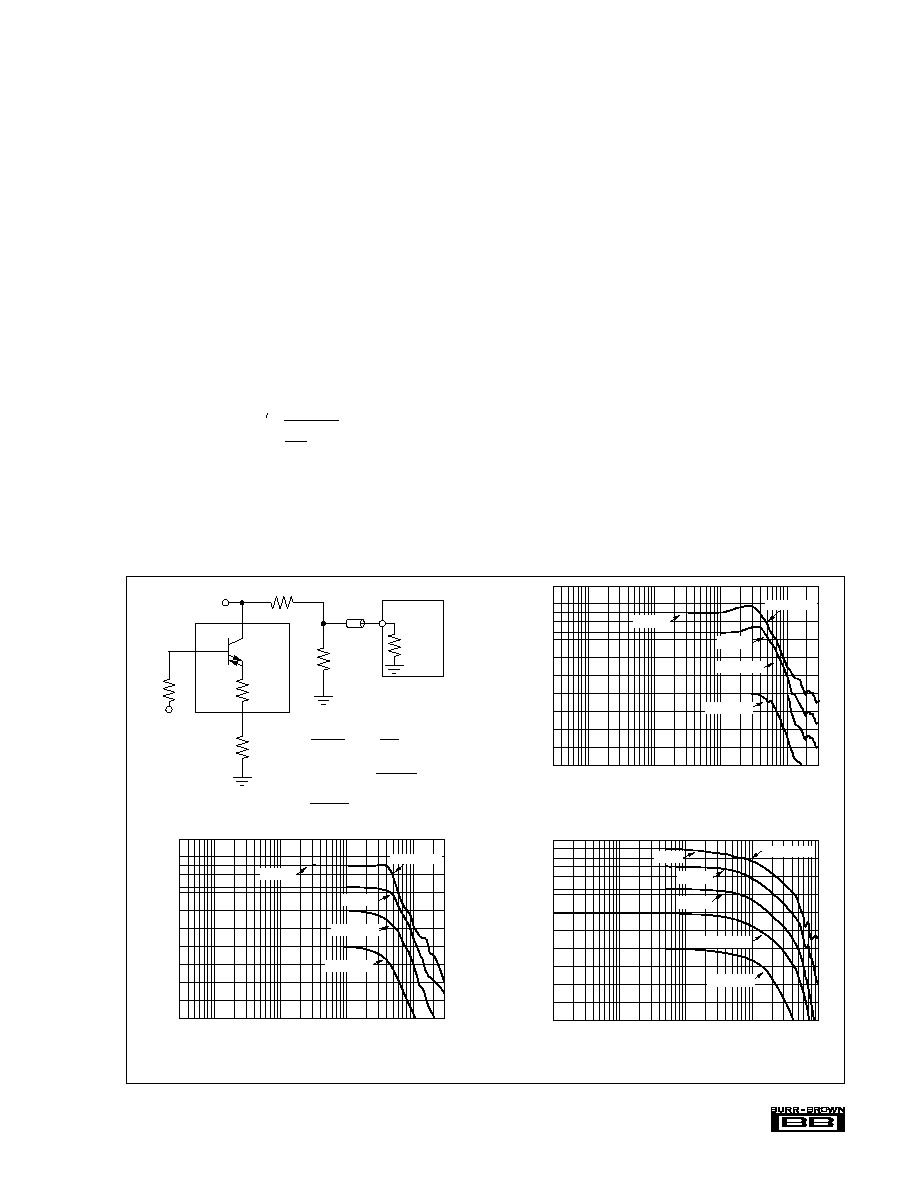
The OPA660 operates from
±
5V power supplies (
±
6V
maximum). Do not attempt to operate with larger power
supply voltages or permanent damage may occur.
Inputs of the OPA660 are protected with internal diode
clamps as shown in the simplified schematic, Figure 1. These
protection diodes can safely conduct 10mA, continuously
(30mA peak). If input voltages can exceed the power supply
voltages by 0.7V, the input signal current must be limited.
The buffer output is not current-limited or protected. If the
output is shorted to ground, currents up to 60mA could flow.
Momentary shorts to ground (a few seconds) should be
avoided, but are unlikely to cause permanent damage. The
same cautions apply to the OTA section when connected as
a buffer (see Basic Applications Circuits, Figure 6b).
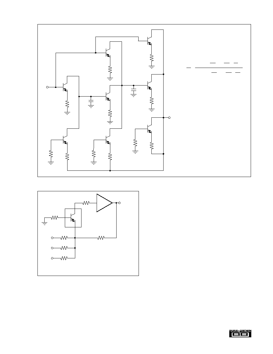
FIGURE 1. Simplified Circuit Diagram.
9
®
OPA660
BUFFER SECTION--AN OVERVIEW
The buffer section of the OPA660 is an open-loop buffer
consisting of complementary emitter-followers. It uses no
feedback, so its low frequency gain is slightly less than unity
and somewhat dependent on loading. It is designed prima-
rily for interstage buffering. It is not designed for driving
long cables or low impedance loads (although with small
signals, it may be satisfactory for these applications).
TRANSCONDUCTANCE
(OTA) SECTION--AN OVERVIEW
The symbol for the OTA section is similar to a transistor.
Applications circuits for the OTA look and operate much
like transistor circuits--the transistor, too, is a voltage-
controlled current source. Not only does this simplify the
understanding of applications circuits, but it aids the circuit
optimization process. Many of the same intuitive techniques
used with transistor designs apply to OTA circuits as well.
The three terminals of the OTA are labeled B, E, and C. This
calls attention to its similarity to a transistor, yet draws
distinction for clarity.
While it is similar to a transistor, one essential difference is
the sense of the C output current. It flows out the C terminal
for positive B-to-E input voltage and in the C terminal for
negative B-to-E input voltage. The OTA offers many advan-
tages over a discrete transistor. The OTA is self-biased,
simplifying the design process and reducing component
count. The OTA is far more linear than a transistor.
Transconductance of the OTA is constant over a wide range
of collector currents--this implies a fundamental improve-
ment of linearity.
BASIC CONNECTIONS
Figure 2 shows basic connections required for operation.
These connections are not shown in subsequent circuit
diagrams. Power supply bypass capacitors should be located
as close as possible to the device pins. Solid tantalum
capacitors are generally best. See "Circuit Layout" at the end
of the applications discussion and Figure 26 for further
suggestions on layout.
QUIESCENT CURRENT CONTROL PIN
The quiescent current of the OPA660 is set with a resistor,
R
Q
, connected from pin 1 to V. It affects the operating
currents of both the buffer and OTA sections. This controls
the bandwidth and AC behavior as well as the
transconductance of the OTA section.
R
Q
= 250
sets approximately 20mA total quiescent current at
25
°
C. With a fixed 250
resistor, process variations could
cause this current to vary from approximately 16mA to 26mA.
It may be appropriate in some applications to trim this resistor
to achieve the desired quiescent current or AC performance.
Applications circuits generally do not show resistor, R
Q
,
but it is required for proper operation.
With a fixed R
Q
resistor, quiescent current increases with
temperature (see typical performance curve, Quiescent Current
vs Temperature). This variation of current with temperature
holds the transconductance, gm, of the OTA relatively con-
stant with temperature (another advantage over a transistor).
It is also possible to vary the quiescent current with a control
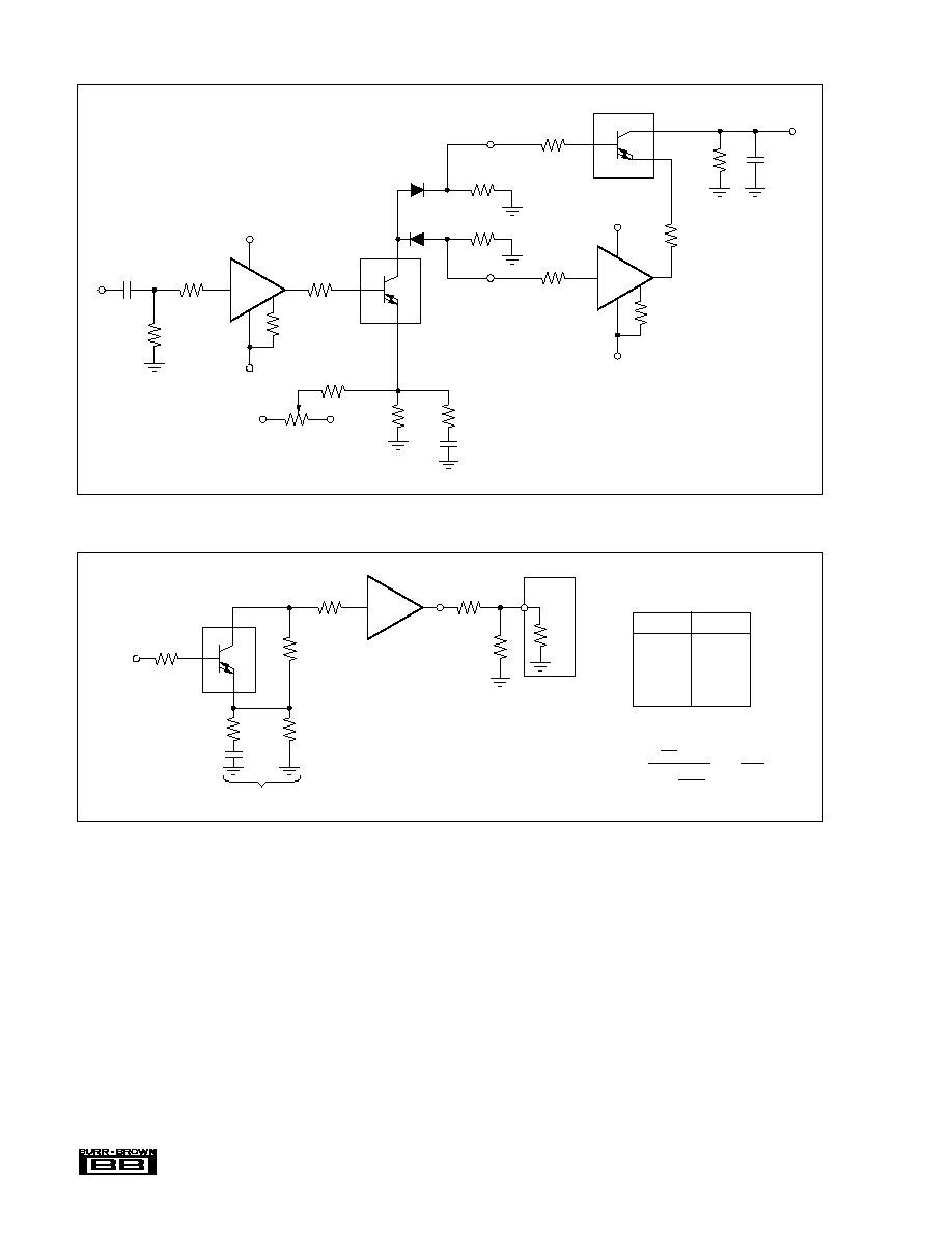
signal. The control loop in Figure 3 shows a 1/2 of a REF200
current source used to develop 100mV on R
1
. The loop
forces 100mV to appear on R
2
. Total quiescent current of the
OPA660 is approximately 85 · I
1
, where I
1
is the current
made to flow out of pin 1.
FIGURE 2. Basic Connections.
50k
100
1
4
V
CC
I
1
425
R
2
1/2
OPA1013
(1)
1/2 REF200
100µA
V+
1k
R
1
Internal
Current Source
Circuitry
I 85 · I
= 85 · (100µA)
= 20mA
Q
1
R
1
R
2
NOTE: (1) Requires input common-mode range and
output swing close to V, thus the choice of OPA1013.
OPA660
FIGURE 3. Optional Control Loop for Setting Quiescent
Current.
With this control loop, quiescent current will be nearly
constant with temperature. Since this differs from the tem-
perature-dependent behavior of the internal current source,
other temperature-dependent behavior may differ from that
shown in typical performance curves.
The circuit of Figure 3 will control the I
Q
of the OPA660
somewhat more accurately than with a fixed external resis-
tor, R
Q
. Otherwise, there is no fundamental advantage to
1
2
3
4
8
7
6
5
+
2.2µF
Solid
Tantalum
5V
(1)
250
R
Q
R = 250
sets roughly
I 20mA
Q
Q
+
Solid
Tantalum
+5V
(1)
NOTE: (1) V
S
= ±6V absolute max.
1
2.2µF
10nF
470pF
470pF
10nF
(25
to
200
)
R
B
(25
to 200
)
R
B
10
®
OPA660
R
B
R
L
R
B
R
E
V
V+
V
I
V
O
(a) Common-Emitter Amplifier
V
O
100
OTA
V
I
B
E
R
L
R
E
Non-Inverting Gain
(b) Common-E Amplifier
Inverting Gain
V several volts
OS
3
2
C
8
Transconductance varies over temperature.
Transconductance remains constant over temperature.
V
OS
0
V
V+
V
I
V
O
(a) Common-Collector Amplifier
(Emitter Follower)
V
O
100
OTA
V
I
(b) Common-C Amplifier
(Buffer)
OS
G 1
V 0.7V
OS
G 1
V 0
B
3
C
8
R
E
R
E
R
O
=
1
g
m
G =
1
1 +
1
g
m
¥
R
E
1
E
2
using this more complex biasing circuitry. It does, however,
demonstrate the possibility of signal-controlled quiescent
current. This may suggest other possibilities such as AGC,
dynamic control of AC behavior, or VCO.
Figure 4 shows logic control of pin 1 used to disable the
OPA660. Zero/5V logic levels are converted to a 1mA/0mA
current connected to pin 1. The 1mA current flowing in R
Q
increases the voltage at pin 1 to approximately 1V above the
5V rail. This will reduce I
Q
to near zero, disabling the
OPA660.
BASIC APPLICATIONS CIRCUITS
Most applications circuits for the OTA section consist of a
few basic types which are best understood by analogy to a
transistor. Just as the transistor has three basic operating
modes--common emitter, common base, and common col-
lector--the OTA has three equivalent operating modes com-
mon-E, common-B, and common-C. See Figures 5, 6, and 7.
50k
100
1
4
5V
I
C
250
R
Q
Internal
Current Source
Circuitry
OPA660
2N2907
+5V
I = 0: OPA660 On
I 1mA: OPA660 Off
C
C
0/5V
Logic In
5V: OPA660 On
4.7k
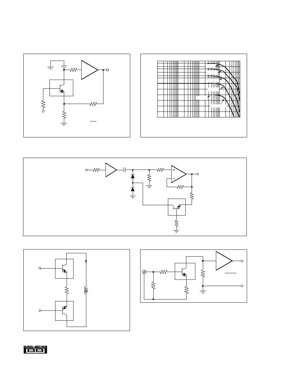
FIGURE 7. Common-Base vs Common-B Amplifier.
FIGURE 6. Common-Collector vs Common-C Amplifier.
FIGURE 5. Common-Emitter vs Common-E Amplifier.
FIGURE 4. Logic-Controlled Disable Circuit.
Inverting Gain
V
I
V
O
(a) Common-Base
Amplifier
OTA
V
I
(b) Common-B Amplifier
OS
R
L
Non-Inverting Gain
V several volts
R
E
V
O
R
L
R
E
B
E
3
2
C
8
G =
R
L
R
E
+
g
m
1
R
L
R
E
V
OS
0
V+
100
11
®
OPA660
A positive voltage at the B, pin 3, causes a positive current
to flow out of the C, pin 8. Figure 5b shows an amplifier
connection of the OTA, the equivalent of a common-emitter
transistor amplifier. Input and output can be ground-refer-
enced without any biasing. Due to the sense of the output
current, the amplifier is non-inverting. Figure 8 shows the
amplifier with various gains and output voltages using this
configuration.
Just as transistor circuits often use emitter degeneration,
OTA circuits may also use degeneration. This can be used to
reduce the effect that offset voltage and offset current might
otherwise have on the DC operating point of the OTA. The
E-degeneration resistor may be bypassed with a large ca-
pacitor to maintain high AC gain. Other circumstances may
suggest a smaller value capacitor used to extend or optimize
high-frequency performance.
The transconductance of the OTA with degeneration can be
calculated by--
Figure 6b shows the OTA connected as an E-follower--a
voltage buffer. The buffer formed by this connection per-
forms virtually the same as the buffer section of the OPA660
(the actual signal path is identical).
It is recommended to use a low value resistor in series with
the B OTA and buffer inputs. This reduces any tendency to
oscillate and controls frequency response peaking. Values
from 25
to 200
are typical.
Figure 7 shows the Common-B amplifier. This configura-
tion produces an inverting gain, and a low impedance input.
This low impedance can be converted to a high impedance
by inserting the buffer amplifier in series.
CIRCUIT LAYOUT
The high frequency performance of the OPA660 can be
greatly affected by the physical layout of the circuit. The
following tips are offered as suggestions, not dogma.
· Bypass power supplies very close to the device pins. Use
a combination between tantalum capacitors (approxi-
mately 2.2
µ
F) and polyester capacitors. Surface-mount
types are best because they provide lowest inductance.
· Make short, wide interconnection traces to minimize
series inductance.
· Use a large ground plane to assure that a low impedance
ground is available throughout the layout.
· Do not extend the ground plane under high impedance
nodes sensitive to stray capacitance.
· Sockets are not recommended because they add signifi-
cant inductance.
FIGURE 8. Common-E Amplifier Performance.
OTA
R
E
3
8
2
R
G = , r =
At I = 20mA r = = 8
G = at I = 20mA
R
L
R + r
E
E
E
1
125mA/V
Q
E
1
gm
R
L
R + 8
E
Q
R
L
= R
L1
+ R
L2
|| R
IN
R
L1
r
E
R
1
100
L2
R
IN
Network
Analyzer
50
V
I
V
O
15
10
5
0
5
10
15
20
25
30
1M
10M
100M
1G
Frequency (Hz)
Output Voltage (dB)
200mVp-p
2.8Vp-p
3dB Point
1.4Vp-p
600mVp-p
I
Q
= 20mA R
1
= 100
R
E
= 51
R
L
= 50
Gain = 1
20
300k
3G
15
10
5
0
5
10
15
20
25
30
1M
10M
100M
1G
Output Voltage (dB)
200mVp-p
2.8Vp-p
3dB Point
1.4Vp-p
600mVp-p
Frequency (Hz)
I
Q
= 20mA R
1
= 100
R
E
= 51
R
L
= 100
Gain = 2
20
300k
3G
15
10
5
0
5
10
15
20
25
30
1M
10M
100M
1G
Output Voltage (dB)
Frequency (Hz)
I
Q
= 20mA R
1
= 100
R
E
= 51
R
L
= 500
Gain = 10
20
100k
200mVp-p
1.4Vp-p
600mVp-p
5Vp-p
2.8Vp-p
3dB Point
1
g =
m
g
m
+ R
E
1
12
®
OPA660
20
20
20
25
V
OUT
V
IN
R
1
40.2
R
2
100k
CCII
B
E
C
2
8
3
D
1
, D
2
= 1N4148
R
Q
= 1k
· The OTA amplifier works as a current conveyor
(CCII) in this circuit, with a current gain of 1.
· R
1
and C
1
set the DC restoration time constant.
· D
1
adds a propagation delay to the DC restoration.
· R
2
and C
1
set the decay time constant.
OPA650
C
1
100pF
D
1
D
2
+1
5
6
· Use low-inductance components. Some film resistors are
trimmed with spiral cuts which increase inductance.
· Use surface-mount components--they generally provide
the lowest inductance.
· A resistor (25
to 200
) in series with the buffer and/or
B input may help reduce oscillations and peaking.
· Use series resistors in the supply lines to decouple mul-
tiple devices.
OTA
V
I
B
E
C
V
O
R
5
3
8
2
22
5
6
R
4
200
R = 250 (I 20mA)
Q
Q
G = 1 + 10
R
4
R
5
+1
R
2
R
1
47
C
1
56
FIGURE 10. Current-Feedback Amplifier Frequency
Response, G = 10.
FIGURE 9. Current-Feedback Amplifier.
15
10
5
0
5
10
15
20
25
1M
10M
100M
1G
Frequency (Hz)
Output Voltage (dB)
OPA660 CURRENT-FEEDBACK
I
Q
= 20mA R
1
= 47
R
2
= 56
R
4
= 200
R
5
= 22
Gain = 10
20
30
2.8Vp-p
0.6Vp-p
1.4Vp-p
5Vp-p
0.2Vp-p
3dB Point
100k
FIGURE 12. High Speed Current Driver (bridge combina-
tion for increased output voltage capability).
FIGURE 13. Cable Amplifier.
OTA
V
I
B
E
C
V
O
R
E
3
8
2
42
5
6
+1
150
150
50
R = 250 (I 20mA)
Q
Q
R
L
G = +3
R
L
R + r
E
E
OTA
B
C
3
8
+IN
2
E
OTA
B
E
3
2
IN
C
8
R
E
Tuning Coil
Magnetic Head
Driver Transformer
I
O
FIGURE 11. DC Restorer Circuit.
13
®
OPA660
FIGURE 14. Comparator (Low Jitter).
FIGURE 15. High Speed Current Driver.
OTA
B
E
C
3
8
2
180
V
I
OTA
B
E
C
3
8
2
180
I
O1
I
O1
R
E
50
R
E
50
I
O
= I
O1
+ I
O2
Diode
22
1k
Q
1
Q
2
22
+5V
Q
1
, Q
2
: 2N3906
+I
B
R
2
100
V
I
+1
5
6
OTA
R
3
100
5
BUF600
1
5V
+5V
R
1
100
R
C5
150
3
2
R
4
150
4
R
5
47
C
3
2.2µF
V
O
C
3
4
7
5V
+5V
R
Q
250
C
3
2.2µF
R
8
27k
C
8
D
1
D
2
0.5...2.5pF
R
6
47k
R
2
10k
+5V
5V
Offset
Trim
8
1
DMF3068A
Propagation Delay Time = 5ns
Rise Time = 1.5ns
2.2µF
C
3
2.2µF
14
®
OPA660
R
3
51
R
6
150
R
6
150
R
7
51
+5V
2.2pF
10nF
7
3
5
4
1
6
2
OPA660
+1
OTA
8
R
9
240
R
8
43
R
16
560
2.2µF
10nF
5V
18pF
R
10
150
4
1
8
5
22pF
10nF
2.2µF
10nF
R
11
51
V
O
+5V
5V
C
5
G = = 4
Rg
R
8
+ r
E
r
E
= 1/gm
BUF601
+V
I
V
I
OTA
B
E
C
3
8
2
5
6
+1
50
780
50k
620
V
I
200
27pF
820
1µF
V
O
5V
+5V
OTA
B
C
3
8
V
I
180
2
E
1
1 +
2g
m
· (R
E
+ R
IN
)
1
G =
1; R
O
=
2g
m
1
R
IN
50
Network
Analyzer
33pF
47
V
O
50
R
E
V
O
f
3dB
±
100mV
351MHz
±
300mV
374MHz
±
700mV
435MHz
±
1.4V
460MHz
±
2.5V
443MHz
FIGURE 19. CMRR and Bandwidth of the Differential Amplifier
FIGURE 18. 400MHz Differential Amplifier
FIGURE 16. Voltage Buffer with Doubled-Output Current.
1M
10M
100M
1G
Frequency (Hz)
300k
3G
10
0
10
20
30
10
I
Q
= 20mA, G = +4V/V
with C
5
without C
5
70
20
30
40
50
60
Gain (dB)
CMRR
FIGURE 17. Integrator for ns-pulses.
15
®
OPA660
FIGURE 20. High Frequency Universal Active Filter.
FIGURE 21. Video Luminance Matrix.
1
B
E
C
V
I
R
1
4
B
E
C
R
1S
5
B
E
C
R
2S
8
B
E
C
R
3S
6
B
E
C
R
1M
7
B
E
C
R
2M
2
B
E
C
R
2
3
B
E
C
R
3
C
1
C
2
V
O
V
O
s
2
C
1
C
2
R
1M
R
3
+ sC
1
R
2
R
1
V
I
s
2
C
1
C
2
R
1M
R
2M
+ sC
1
R
1M
1
Lowpass R
2
= R
3
=
Highpass R
1
= R
2
=
Bandpass R
1
= R
3
=
Band Rejection R
2
=
, R
1
= R
3
Allpass R
1
= R
1S
, R
2
= R
2S
, R
3
= R
3S
R
2S
R
1S
+
R
2M
R
3S
R
1M
1
+
TRANSFER CHARACTERISTICS
F(p) = =
R
B
R
B
R
B
OTA
B
E
C
3
8
2
5
6
+1
150
120
200
V
LUMINANCE
V
RED
665
(1)
V
GREEN
340
(1)
V
BLUE
1820
(1)
R
Q
= 500
(I
Q
20mA)
NOTE: (1) Resistors shown are 1% values that
produce 30%/59%/11% R/G/B mix.
16
®
OPA660
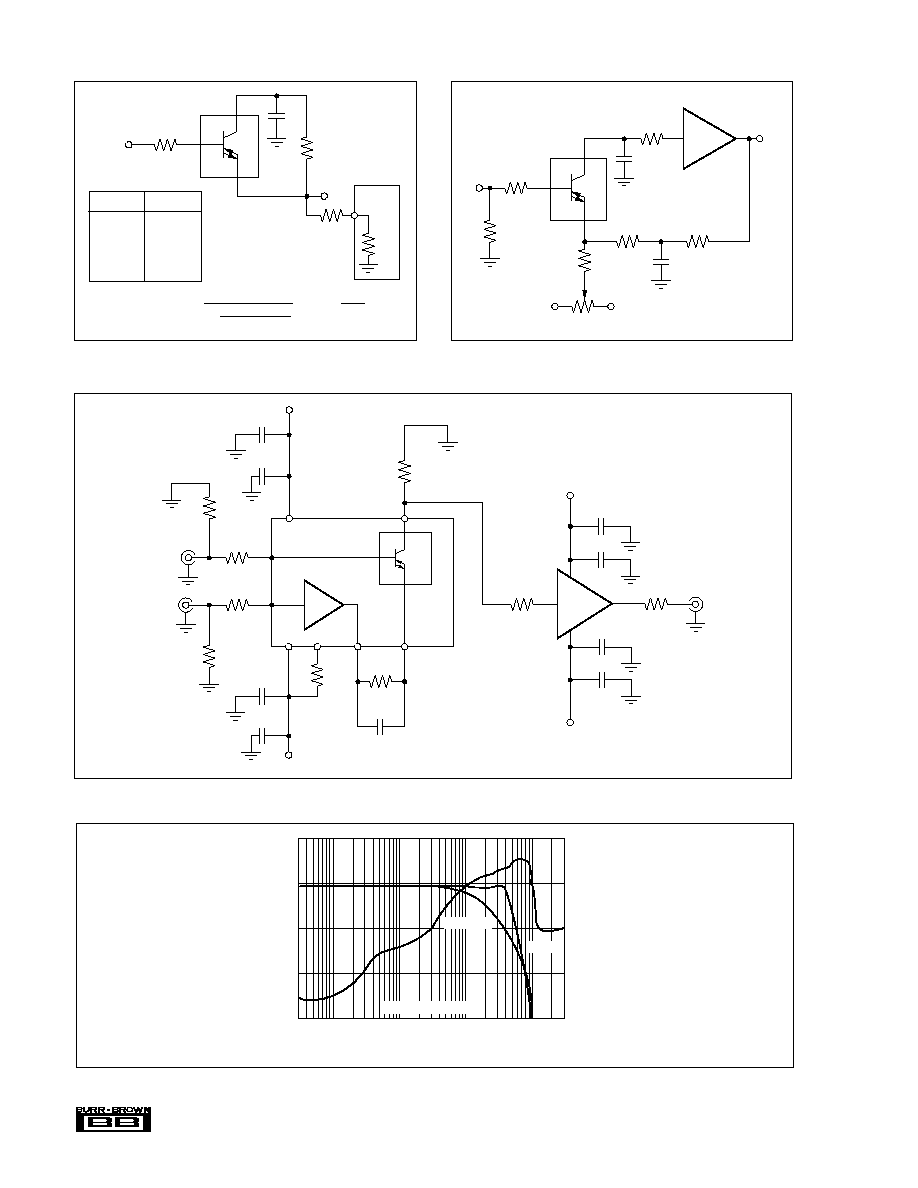
FIGURE 23. Direct-Feedback Amplifier.
OTA
B
E
C
3
8
5
6
+1
100
120
V
I
390
200
2
R
P
R
IN
Network
Analyzer
100
82
6.4pF
C
P
50
R
6
68
R
4
R
2
R
3
I
Q
= 20mA
X
E
G = = 1 +
2
R
3
2 · g
m
1
+ R
5
R
5
+
R
3
2R
5
R
1
R
5
V
O
V
O
f
3dB
±
100mV
331MHz
±
300mV
362MHz
±
700mV
520MHz
±
1.4V
552MHz
±
2.5V
490MHz
FIGURE 22. Signal Envelope Detector (Full-Wave Rectifier).
OTA
3
8
2
20k
3
8
2
V
I
220
OTA
3
8
2
V
O
INT
10
180
4
+1
15nF
1µF
7
5
1.2k
6
5V
V
O
100
+V
O
290
4
+1
7
5
1.2k
1
5V
100
+5V
6
180
390
220
220
12k
5k
Offset Trim
+
33pF
IN6263
IN6263
+5V
17
®
OPA660
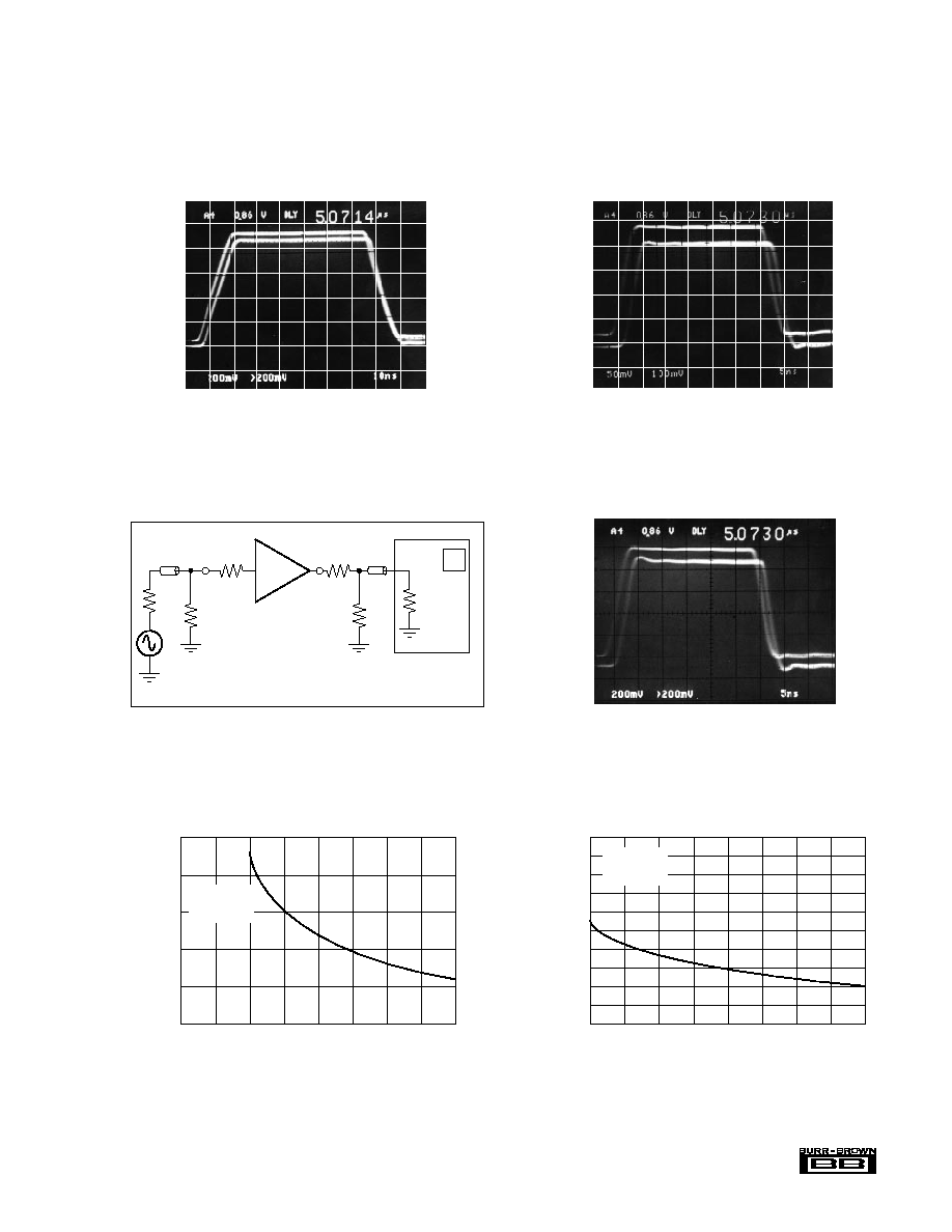
FIGURE 24. Frequency Response Direct-Feedback Amplifier.
FIGURE 25. Direct-Feedback Amplifier Small-Signal Pulse
Response.
Gain = 3, t
R
t
F
= 2ns, V
I
= 100mVpp
0
5
10
15
20
25
30
35
40
45 50
Time (ns)
FIGURE 26. Direct-Feedback Amplifier Large-Signal Pulse
Response.
Gain = 3, V
I
= 2Vp-p, t
R
= t
F
= 2ns
V
O
(V)
0
5
10
15
20
25
30
35
40
45 50
Time (ns)
OTA
B
E
C
3
8
2
160
V
I
R
4P
R
4
R
3
R
IN
Network
Analyzer
51
75
5.6pF
C
4P
I
Q
= 20mA
56
180
V
O
50
R
2
R
1
FIGURE 27. Forward Amplifier.
V
O
f
3dB
±
100mV
351MHz
±
300mV
374MHz
±
700mV
435MHz
±
1.4V
460MHz
±
2.5V
443MHz
SPICE MODELS
Computer simulation using SPICE models is often useful
when analyzing the performance of analog circuits and sys-
tems. This is particularly true for video and RF amplifier
circuits, where parasitic capacitance and inductance can have
a major effect on circuit performance. SPICE models are
available from Burr-Brown.
FIGURE 28. Frequency Response Forward Amplifier.
3V
+3V
0V
0V
+150mV
150mV
V
O
(V)
15
10
5
0
5
10
15
20
25
1M
10M
100M
1G
Output Voltage (dB)
Frequency (Hz)
OPA660 DIRECT FEEDBACK
R
1
= 100
R
2
= 120
R
3
= 390
R
4
= 200
R
5
= 100
R
6
= 68
I
Q
= 20mA R
p
= 82
C
p
= 6.4pF
20
30
0.2Vp-p
5Vp-p
2.8Vp-p
1.4Vp-p
0.6Vp-p
100k
15
10
5
0
5
10
15
20
25
30
1M
10M
100M
1G
Output Voltage (dB)
Frequency (Hz)
OPA660 OTA FORWARD AMPLIFIER
I
Q
= 20mA R
1
= 160
R
4
= 51
R
2
= 180
R
3
= 56
R
4p
= 75
C
4p
= 5.6pF
20
100k
0.2Vp-p
5Vp-p
2.8Vp-p
1.4Vp-p
0.6Vp-p
18
®
OPA660
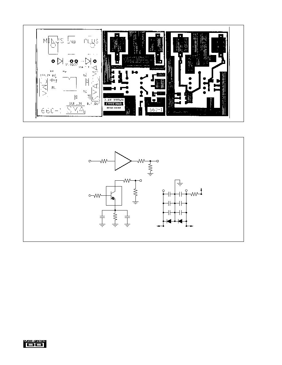
FIGURE 29. Evaluation Circuit Silk Screen and Board Layouts.
FIGURE 30. Evaluation Circuit Diagram.
OTA
B
E
C
3
2
R
4
51
R
2
24
R
1
100
C
1
C
2
3.3nF
OTA In
8
5
6
+1
R
6
470
R
5
160
R
3
51
BUF In
OTA Out
BUF Out
1N4007
R
QC
820
7
1
+5V
470pF
4
5V
470pF
10nF
10nF
2.2µF
2.2µF
R
7
56
2.2µF