 | –≠–ª–µ–∫—Ç—Ä–æ–Ω–Ω—ã–π –∫–æ–º–ø–æ–Ω–µ–Ω—Ç: OPA693ID | –°–∫–∞—á–∞—Ç—å:  PDF PDF  ZIP ZIP |
Document Outline
- FEATURES
- APPLICATIONS
- DESCRIPTION
- OPA693 RELATED PRODUCTS
- ABSOLUTE MAXIMUM RATINGS(1)
- PACKAGE/ORDERING INFORMATION
- PIN CONFIGURATION
- ELECTRICAL CHARACTERISTICS: VS = +/-5V
- ELECTRICAL CHARACTERISTICS: VS = +5V
- TYPICAL CHARACTERISTICS: VS = ±5V
- TYPICAL CHARACTERISTICS: VS = +5V
- APPLICATION INFORMATION
- WIDEBAND BUFFER OPERATION
- SINGLE-SUPPLY OPERATION
- SINGLE-SUPPLY ADC INTERFACE
- WIDEBAND UNITY GAIN BUFFER WITH IMPROVED FLATNESS
- WIDEBAND, DC-COUPLED, SINGLE-TO-DIFFERENTIAL CONVERSION
- HIGH-FREQUENCY ACTIVE FILTERS
- DESIGN-IN TOOLS
- OPERATING SUGGESTIONS
- GAIN SETTING
- OUTPUT CURRENT AND VOLTAGE
- DRIVING CAPACITIVE LOADS
- DISTORTION PERFORMANCE
- GAIN ACCURACY AND LINEARITY
- NOISE PERFORMANCE
- DC ACCURACY AND OFFSET CONTROL
- DISABLE OPERATION
- THERMAL ANALYSIS
- BOARD LAYOUT GUIDELINES
- INPUT AND ESD PROTECTION
OPA6
93
OPA6
93
OPA693
SBOS285 ≠ OCTOBER 2003
www.ti.com
DESCRIPTION
The OPA693 provides an easy to use, broadband, fixed gain
buffer amplifier. Depending on the external connections, the
internal resistor network may be used to provide either a
fixed gain of +2 video buffer or a gain of
±
1 voltage buffer.
Operating on a low 13mA supply current, the OPA693 offers
a slew rate (2500V/
µ
s) and bandwidth (> 700MHz) normally
associated with a much higher supply current. A new output
stage architecture delivers high output current with a minimal
headroom and crossover distortion. This gives exceptional
single-supply operation. Using a single +5V supply, the
OPA693 can deliver a 2.5V
PP
swing with over 90mA drive
current and 500MHz bandwidth at a gain of +2. This combi-
nation of features makes the OPA693 an ideal RGB line
driver or single-supply undersampling Analog-to-Digital Con-
verter (ADC) input driver.
The OPA693's low 13mA supply current is precisely trimmed
at 25
∞
C. This trim, along with low drift over temperature,
ensures lower maximum supply current than competing
products that report only a room temperature nominal supply
current. System power may be further reduced by using the
optional disable control pin. Leaving this disable pin open, or
holding it HIGH, gives normal operation. This optional dis-
able allows the OPA693 to fit into existing video buffer
layouts where the disable pin is unconnected to get improved
performance with no board changes. If pulled LOW, the
OPA693 supply current drops to less than 170
µ
A while the
output goes into a high impedance state. This feature may be
used for power savings.
The low gain stable current-feedback architecture used in the
OPA693 is particularly suitable for high full-power bandwidth
cable driving requirements. Where the additional flexibility of
an op amp is required, consider the OPA695 ultra-wideband
current feedback op amp. Where a unity gain stable voltage
feedback op amp with very high slew rate is required,
consider the OPA690.
FEATURES
q
VERY HIGH BANDWIDTH (G = +2): 700MHz
q
FLEXIBLE SUPPLY RANGE:
+5V to +12V Single Supply
±
2.5V to
±
6V Dual Supplies
q
INTERNALLY FIXED GAIN: +2 or
±
1
q
LOW SUPPLY CURRENT: 13mA
q
LOW DISABLED CURRENT: 120
µ
A
q
HIGH OUTPUT CURRENT:
±
120mA
q
OUTPUT VOLTAGE SWING:
±
4.1V
q
SOT23-6 AVAILABLE
Copyright © 2002-2003, Texas Instruments Incorporated
Ultra-Wideband, Fixed Gain
Video BUFFER AMPLIFIER with Disable
Please be aware that an important notice concerning availability, standard warranty, and use in critical applications of
Texas Instruments semiconductor products and disclaimers thereto appears at the end of this data sheet.
APPLICATIONS
q
BROADBAND VIDEO LINE DRIVERS
q
MULTIPLE LINE VIDEO DA
q
PORTABLE INSTRUMENTS
q
ADC BUFFERS
q
HIGH FREQUENCY ACTIVE FILTERS
q
HFA1112 IMPROVED DROP-IN
OPA693 RELATED PRODUCTS
SINGLES
DUALS
TRIPLES
Voltage Feedback
OPA690
OPA2690
OPA3690
Current Feedback
OPA691
OPA2691
OPA3691
Fixed Gain
OPA692
--
OPA3692
> 900MHz
OPA695
--
--
75
Video
Out
Video
Out
75
RG-59
75
75
RG-59
75
300
300
1
2
3
4
8
7
6
5
DIS
OPA693
SO-8
G = +2
700MHz, 2-Output Component Video DA
+5V
-
5V
Video
In
PRODUCTION DATA information is current as of publication date.
Products conform to specifications per the terms of Texas Instruments
standard warranty. Production processing does not necessarily include
testing of all parameters.
All trademarks are the property of their respective owners.
OPA693
2
SBOS285
www.ti.com
SPECIFIED
PACKAGE
TEMPERATURE
PACKAGE
ORDERING
TRANSPORT
PRODUCT
PACKAGE-LEAD
DESIGNATOR
(1)
RANGE
MARKING
NUMBER
MEDIA, QUANTITY
OPA693
SO-8
D
≠40
∞
C to +85
∞
C
OPA693D
OPA693ID
Rails, 100
"
"
"
"
"
OPA693IDR
Tape and Reel, 2500
OPA693
SOT23-6
DBV
≠40
∞
C to +85
∞
C
C59
OPA693IDBVT
Tape and Reel, 250
"
"
"
"
"
OPA693IDBVR
Tape and Reel, 3000
NOTE: (1) For the most current specifications and package information, refer to our web site at www.ti.com.
ABSOLUTE MAXIMUM RATINGS
(1)
Power Supply ...............................................................................
±
6.5V
DC
Internal Power Dissipation
(2)
............................ See Thermal Information
Differential Input Voltage ..................................................................
±
1.2V
Input Voltage Range ............................................................................
±
V
S
Storage Temperature Range: D, DVB ........................... ≠40
∞
C to +125
∞
C
Lead Temperature (soldering, 10s) .............................................. +300
∞
C
Junction Temperature (T
J
) ........................................................... +150
∞
C
ESD Rating (Human Body Model) .................................................. 2000V
(Charge Device Model) ............................................... 1000V
(Machine Model) ............................................................ 100V
NOTES:: (1) Stresses above these ratings may cause permanent damage.
Exposure to absolute maximum conditions for extended periods may degrade
device reliability. These are stress ratings only, and functional operation of the
device at these or any other conditions beyond those specified is not implied.
(2) Packages must be derated based on specified
JA
. Maximum T
J
must be
observed.
ELECTROSTATIC
DISCHARGE SENSITIVITY
This integrated circuit can be damaged by ESD. Texas Instru-
ments recommends that all integrated circuits be handled with
appropriate precautions. Failure to observe proper handling
and installation procedures can cause damage.
ESD damage can range from subtle performance degrada-
tion to complete device failure. Precision integrated circuits
may be more susceptible to damage because very small
parametric changes could cause the device not to meet its
published specifications.
PIN CONFIGURATION
Top View
SO
Top View
SOT23
PACKAGE/ORDERING INFORMATION
1
2
3
4
8
7
6
5
DIS
+V
S
Output
NC
R
F
300
R
G
300
NC
-
IN
+IN
-
V
S
NC = No Connection
1
2
3
6
5
4
Output
-
V
S
+IN
+V
S
DIS
-
IN
R
F
300
R
G
300
1
2
3
6
5
4
Pin Orientation/Package Marking
C59

OPA693
3
SBOS285
www.ti.com
ELECTRICAL CHARACTERISTICS:
V
S
=
±
5V
Boldface limits are tested at 25
∞
C.
G = +2 (≠IN grounded) and R
L
= 100
(see Figure 1 for AC performance only), unless otherwise noted.
OPA693ID, IDBV
TYP
MIN/MAX OVER TEMPERATURE
(1)
0
∞
C to
≠40
∞
C to
MIN/
TEST
PARAMETER
CONDITIONS
+25
∞
C
+25
∞
C
70
∞
C
+85
∞
C
UNITS
MAX
LEVEL
(2 )
AC PERFORMANCE (see Figure 1)
Small-Signal Bandwidth (V
O
< 1.0V
PP
)
G = +1
1400
MHz
typ
C
G = +2
700
510
490
480
MHz
min
B
G = ≠1
700
510
490
480
MHz
typ
C
Bandwidth for 0.2dB Gain Flatness
G = +2, V
O
< 1.0V
PP
, R
L
= 150
400
122
112
108
MHz
min
B
Peaking at a Gain of +1
V
O
< 1.0V
PP
2.5
3.8
4.8
5.2
dB
max
B
Large-Signal Bandwidth
G = +2, V
O
= 4V
PP
400
MHz
typ
C
Slew Rate
G = +2, 4V Step
2500
2200
2100
2000
V/
µ
s
min
B
Rise-and-Fall Time
G = +2, V
O
= 0.5V Step
0.6
0.8
0.8
0.8
ns
max
B
G = +2, V
O
= 5V Step
1.2
1.3
1.3
1.4
ns
max
B
Settling Time to 0.02%
G = +2, V
O
= 2V Step
16
ns
typ
C
Settling Time to 0.1%
G = +2, V
O
= 2V Step
12
ns
typ
C
Harmonic Distortion
G = +2, f = 10MHz, V
O
= 2V
PP
2nd-Harmonic
R
L
= 100
≠69
≠66
≠65
≠64
dBc
max
B
R
L
500
≠82
≠80
≠79
≠78
dBc
max
B
3rd-Harmonic
R
L
= 100
≠83
≠80
≠70
≠69
dBc
max
B
R
L
500
≠96
≠86
≠85
≠82
dBc
max
B
Input Voltage Noise
f > 1MHz
1.8
2
2.7
2.9
nV/
Hz
max
B
Noninverting Input Current Noise
f > 1MHz
18
19
21
22
pA/
Hz
max
B
Inverting Input Current Noise (internal)
f > 1MHz
22
24
26
27
pA/
Hz
max
B
Differential Gain
NTSC, R
L
= 150
0.03
%
typ
C
NTSC, R
L
= 37.5
0.03
%
typ
C
Differential Phase
NTSC, R
L
= 150
0.01
deg
typ
C
NTSC, R
L
= 37.5
0.1
deg
typ
C
DC PERFORMANCE
(3)
Gain Error
G = +1
±
0.2
%
typ
C
G = +2
±
0.3
±
0.9
±
1.0
±
1.1
%
max
A
G = ≠1, R
S
= 0
±
0.2
±
0.8
±
0.9
±
1.0
%
max
B
DC Linearity
V
O
=
±
2, R
L
= 100
, G = +2
0.0016
%
typ
C
Internal R
F
and R
G
Maximum
300
341
345
346
max
A
Minimum
300
264
260
259
min
A
Average Drift
0.03
0.03
%/C
∞
max
B
Input Offset Voltage
V
CM
= 0V
±
0.3
±
2.0
±
2.3
±
2.5
mV
max
A
Average Offset Voltage Drift
V
CM
= 0V
±
5
±
8
µ
V/
∞
C
max
B
Noninverting Input Bias Current
V
CM
= 0V
+15
±
35
±
43
±
45
µ
A
max
A
Average Noninverting Input Bias Current Drift
V
CM
= 0V
170
170
nA/
∞
C
max
B
Inverting Input Bias Current (internal)
V
CM
= 0V
±
20
±
50
±
52
±
54
µ
A
max
A
Average Inverting Input Bias Current Drift
V
CM
= 0V
50
60
nA
∞
C
max
B
INPUT
Common-Mode Input Range
±
3.4
±
3.3
±
3.2
±
3.2
V
min
B
Noninverting Input Impedance
300 || 1.2
k
|| pF
typ
C
OUTPUT
Voltage Output Swing
No Load
±
4.1
±
3.9
±
3.9
±
3.8
V
min
A
100
Load
±
3.8
±
3.7
±
3.7
±
3.6
V
min
A
Current Output, Sourcing
+120
+90
+80
+70
mA
min
A
Current Output, Sinking
≠120
≠90
≠80
≠70
mA
min
A
Closed-Loop Output Impedance
G = +2, f = 100kHz
0.18
typ
C
(1) Junction temperature = ambient temperature for low temperature limit and +25
∞
C specifications. Junction temperature = ambient temperature +20
∞
C at high
temperature limit specifications.
(2) Test Levels: (A) 100% tested at +25
∞
C. Over temperature limits by characterization and simulation.
(B) Limits set by characterization and simulation.
(C) Typical value only for information.
(3) Current is considered positive out-of-node. V
CM
is the input common-mode voltage.
OPA693
4
SBOS285
www.ti.com
ELECTRICAL CHARACTERISTICS:
V
S
=
±
5V (Cont.)
Boldface limits are tested at 25
∞
C.
G = +2 (≠IN grounded) and R
L
= 100
(see Figure 1 for AC performance only), unless otherwise noted.
OPA693ID, IDBV
TYP
MIN/MAX OVER TEMPERATURE
(1)
0
∞
C to
≠40
∞
C to
MIN/
TEST
PARAMETER
CONDITIONS
+25
∞
C
+25
∞
C
70
∞
C
+85
∞
C
UNITS
MAX
LEVEL
(2 )
DISABLE/POWER DOWN ( DIS Pin)
Power-Down Supply Current (+V
S
)
V
DIS
= 0V
≠70
≠170
≠186
≠192
µ
A
max
A
Disable Time
V
IN
= +1V
DC
3
µ
s
typ
C
Enable Time
V
IN
= +1V
DC
25
ns
typ
C
Off Isolation
G = +2, 5MHz
70
dB
typ
C
Output Capacitance in Disable
4
pF
typ
C
Turn-On Glitch
G = +2, R
L
= 150
, V
IN
= 0V
DC
±
100
mV
typ
C
Turn-Off Glitch
G = +2, R
L
= 150
, V
IN
= 0V
DC
±
20
mV
typ
C
Enable Voltage
+V
S
= +5V
3.3
3.5
3.6
3.7
V
min
A
Disable Voltage
+V
S
= +5V
1.8
1.7
1.6
1.5
V
max
A
Control Pin Input Bias Current
V
DIS
= 0V
75
130
143
149
µ
A
max
A
POWER SUPPLY
Specified Operating Voltage
±
5
V
typ
C
Maximum Operating Voltage Range
±
6
±
6
±
6
V
max
A
Max Quiescent Current
V
S
=
±
5V
13
13.3
13.7
14.1
mA
max
A
Min Quiescent Current
V
S
=
±
5V
13
12.5
11.6
11.0
mA
min
A
Power-Supply Rejection Ratio (+PSRR)
Input Referred
58
54
52
51
dB
min
A
TEMPERATURE RANGE
Specification: D, DBV
≠40 to +85
∞
C
typ
C
Thermal Resistance,
JA
D
SO-8
125
∞
C/W
typ
C
DBV
SOT23-6
150
∞
C/W
typ
C
(1) Junction temperature = ambient temperature for low temperature limit and +25
∞
C specifications. Junction temperature = ambient temperature +20
∞
C at high
temperature limit specifications.
(2) Test Levels: (A) 100% tested at +25
∞
C. Over temperature limits by characterization and simulation.
(B) Limits set by characterization and simulation.
(C) Typical value only for information.
(3) Current is considered positive out-of-node. V
CM
is the input common-mode voltage.
OPA693
5
SBOS285
www.ti.com
ELECTRICAL CHARACTERISTICS:
V
S
= +5V
Boldface limits are tested at +25
∞
C.
G = +2 (≠IN grounded though 0.001
µ
F) and R
L
= 100
to V
S
/2 (see Figure 4 for AC performance only), unless otherwise noted.
OPA693ID, IDBV
TYP
MIN/MAX OVER TEMPERATURE
0
∞
C to
≠40
∞
C to
MIN/
TEST
PARAMETER
CONDITIONS
+25
∞
C
+25
∞
C
(1)
70
∞
C
+85
∞
C
UNITS
MAX
LEVEL
(2 )
AC PERFORMANCE (see Figure 4)
Small-Signal Bandwidth (V
O
< 1.0V
PP
)
G = +1
634
MHz
typ
C
G = +2
526
400
390
380
MHz
min
B
G = ≠1
512
MHz
typ
C
Bandwidth for 0.2dB Gain Flatness
G = +2, V
O
< 1.0V
PP
210
110
100
96
MHz
min
B
Peaking at a Gain of +1
V
O
< 1.0V
PP
1.9
2.6
3.6
3.9
dB
max
B
Large-Signal Bandwidth
G = +2, V
O
= 2V
PP
400
MHz
typ
C
Slew Rate
G = +2, 2V Step
1500
1200
1100
1000
V/
µ
s
min
B
Rise-and-Fall Time
G = +2, V
O
= 0.5V Step
0.8
ns
typ
C
G = +2, V
O
= 2V Step
1.0
ns
typ
C
Settling Time to 0.02%
G = +2, V
O
= 2V Step
16
ns
typ
C
Settling Time to 0.1%
G = +2, V
O
= 2V Step
12
ns
typ
C
Harmonic Distortion
G = +2, f = 10MHz, V
O
= 2V
PP
2nd-Harmonic
R
L
= 100
to V
S
/2
≠66
≠62
≠62
≠61
dBc
max
B
R
L
500
to V
S
/2
≠75
≠69
≠68
≠68
dBc
max
B
3rd-Harmonic
R
L
= 100
to V
S
/2
≠70
≠64
≠63
≠62
dBc
max
B
R
L
500
to V
S
/2
≠69
≠63
≠62
≠61
dBc
max
B
Input Voltage Noise
f > 1MHz
1.8
2
2.7
2.9
nV/
Hz
max
B
Noninverting Input Current Noise
f > 1MHz
18
19
21
22
pA/
Hz
max
B
Inverting Input Current Noise
f > 1MHz
22
24
26
27
pA/
Hz
max
B
DC PERFORMANCE
(3)
Gain Error
G = +1
±
0.2
%
typ
C
G = +2
±
0.5
±
1.2
±
1.3
±
1.4
%
max
A
G = ≠1
±
0.4
±
1.1
±
1.2
±
1.3
%
max
B
Internal R
F
and R
G
Maximum
300
341
345
346
max
B
Minimum
300
264
260
259
min
B
Average Drift
0.03
0.03
0.03
%/C
∞
max
B
Input Offset Voltage
V
CM
= 2.5V
±
0.3
±
2.5
±
2.8
±
3.0
mV
max
A
Average Offset Voltage Drift
V
CM
= 2.5V
±
5
±
8
µ
V/
∞
C
max
B
Noninverting Input Bias Current
V
CM
= 2.5V
+5
±
25
±
33
±
35
µ
A
max
A
Average Noninverting Input Bias Current Drift
V
CM
= 2.5V
±
170
±
170
nA/
∞
C
max
B
Inverting Input Bias Current
V
CM
= 2.5V
±
20
±
50
±
52
±
54
µ
A
max
A
Average Inverting Input Bias Current Drift
V
CM
= 2.5V
±
50
±
60
nA
∞
C
max
B
INPUT
Least Positive Input Voltage
1.6
1.7
1.8
1.8
V
max
B
Most Positive Input Voltage
3.4
3.3
3.2
3.2
V
min
B
Noninverting Input Impedance
300 || 1.2
k
|| pF
typ
C
OUTPUT
Most Positive Output Voltage
No Load
4.1
3.9
3.9
3.8
V
min
A
R
L
= 100
3.9
3.8
3.8
3.7
V
min
A
Least Positive Output Voltage
No Load
0.9
1.1
1.1
1.2
V
max
A
R
L
= 100
1.1
1.2
1.2
1.3
V
max
A
Current Output, Sourcing
+120
+90
+80
+70
mA
min
A
Current Output, Sinking
≠120
≠90
≠80
≠70
mA
min
A
Output Impedance
G = +2, f = 100kHz
0.18
typ
C
(1) Junction temperature = ambient temperature for low temperature limit and +25
∞
C specifications. Junction temperature = ambient temperature +10
∞
C at high
temperature limit specifications.
(2) Test Levels: (A) 100% tested at +25
∞
C. Over temperature limits by characterization and simulation.
(B) Limits set by characterization and simulation.
(C) Typical value only for information.
(3) Current is considered positive out-of-node. V
CM
is the input common-mode voltage.
OPA693
6
SBOS285
www.ti.com
ELECTRICAL CHARACTERISTICS:
V
S
= +5V (Cont.)
Boldface limits are tested at +25
∞
C.
G = +2 (≠IN grounded though 0.001
µ
F) and R
L
= 100
to V
S
/2 (see Figure 4 for AC performance only), unless otherwise noted.
OPA693ID, IDBV
TYP
MIN/MAX OVER TEMPERATURE
0
∞
C to
≠40
∞
C to
MIN/
TEST
PARAMETER
CONDITIONS
+25
∞
C
(1)
+25
∞
C
70
∞
C
+85
∞
C
UNITS
MAX
LEVEL
(2 )
DISABLE/POWER DOWN ( DIS Pin)
Power-Down Supply Current (+V
S
)
V
DIS
= 0
≠95
≠155
≠172
≠180
µ
A
typ
A
Off Isolation
G = +2, 5MHz
65
dB
typ
C
Output Capacitance in Disable
4
pF
typ
C
Turn-On Glitch
G = +2, R
L
= 150
, V
IN
= 2.5V
±
20
mV
typ
B
Turn-Off Glitch
G = +2, R
L
= 150
, V
IN
= 2.5V
±
20
mV
typ
B
Enable Voltage
3.3
3.5
3.6
3.7
V
min
B
Disable Voltage
1.8
1.7
1.6
1.5
V
max
B
Control Pin Input Bias Current (DIS )
V
DIS
= 0
80
137
153
160
µ
A
typ
A
POWER SUPPLY
Specified Single-Supply Operating Voltage
5
V
typ
C
Maximum Single-Supply Operating Voltage
+12
+12
+12
V
max
A
Maximum Quiescent Current
V
S
= +5V
11.5
12.0
12.5
12.9
mA
max
A
Minimum Quiescent Current
V
S
= +5V
11.5
11.0
9.5
9.2
mA
min
A
Power-Supply Rejection Ratio (+PSRR)
Input Referred
57
dB
typ
C
TEMPERATURE RANGE
Specification: D, DBV
≠40 to +85
∞
C
typ
C
Thermal Resistance,
JA
D
SO-8
125
∞
C/W
typ
C
DBV SOT23-6
150
∞
C/W
typ
C
(1) Junction temperature = ambient temperature for low temperature limit and +25
∞
C specifications. Junction temperature = ambient temperature +10
∞
C at high
temperature limit specifications.
(2) Test Levels: (A) 100% tested at +25
∞
C. Over temperature limits by characterization and simulation.
(B) Limits set by characterization and simulation.
(C) Typical value only for information.
(3) Current is considered positive out-of-node. V
CM
is the input common-mode voltage.
OPA693
7
SBOS285
www.ti.com
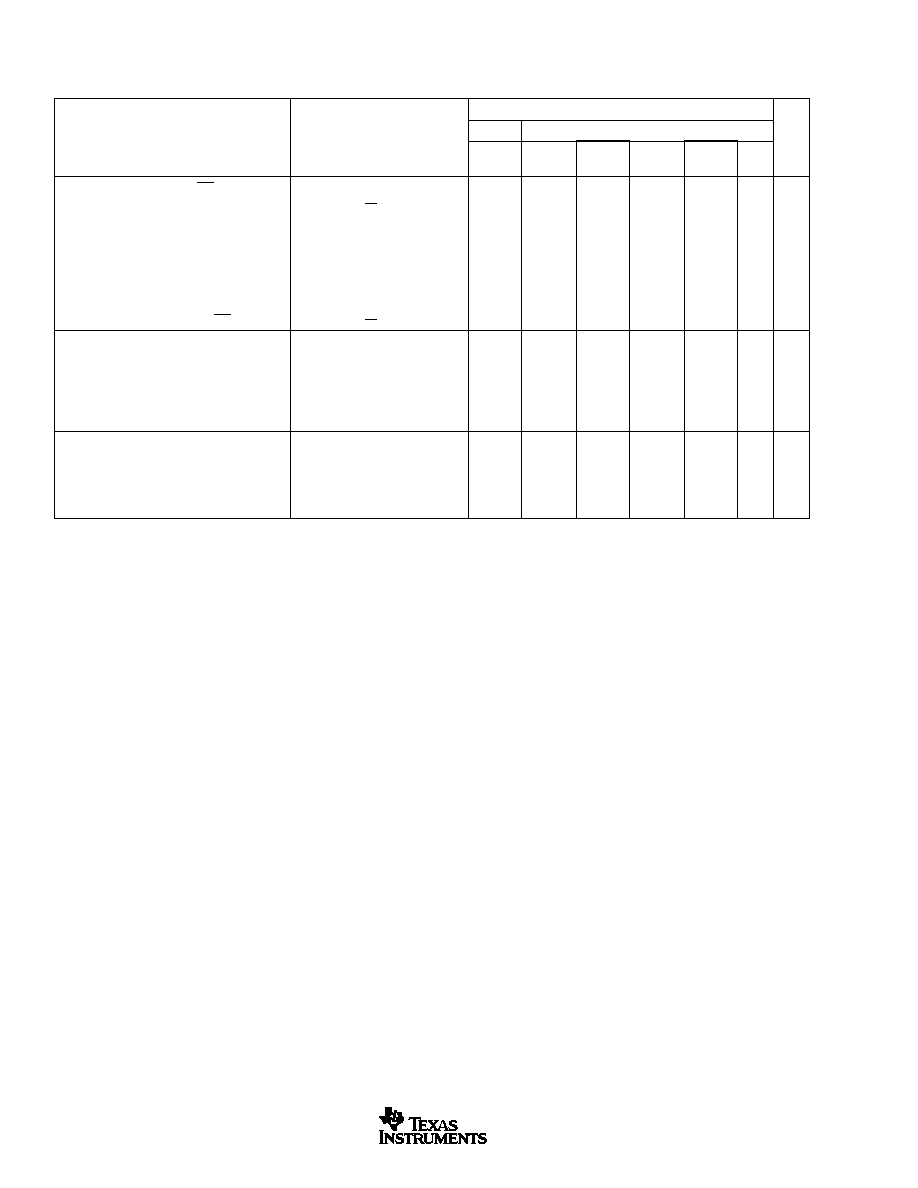
TYPICAL CHARACTERISTICS:
V
S
=
±
5V
At T
A
= +25
∞
C, G = +2, and R
L
= 100
, unless otherwise specified.
Time (2ns/div)
GAIN OF +1 PULSE RESPONSE
Output (V)
3
2
1
0
-
1
-
2
-
3
R
L
= 100
See Figure 2
Large Signal
Small Signal
3
2
1
0
-
1
-
2
-
3
-
4
-
5
-
6
Normalized Gain (dB)
10
100
1000
2000
Frequency (MHz)
SMALL-SIGNAL FREQUENCY RESPONSE
V
O
= 1V
PP
G = +1
G = +2
G =
-
1
8
7
6
5
4
3
2
1
0
-
1
Gain (dB)
0
400
600
200
800
1000
Frequency (MHz)
LARGE-SIGNAL FREQUENCY RESPONSE
G = +2
R
L
= 100
See Figure 1
V
O
= 1V
PP
V
O
= 2V
PP
V
O
= 4V
PP
V
O
= 7V
PP
0.2
0.1
0
-
0.1
-
0.2
-
0.3
-
0.4
Normalized Gain (dB)
0
200
100
300
400
Frequency (MHz)
FREQUENCY RESPONSE FLATNESS vs LOAD
G = +2
V
O
= 1V
PP
See Figure 1
R
L
= 200
R
L
= 150
R
L
= 100
R
L
= 75
1.00
0.75
0.50
0.25
0
-
0.25
-
0.50
-
0.75
-
1.00
Deviation from Linear Phase (
∞
)
0
100
50
150
200
Frequency (MHz)
DEVIATION FROM LINEAR PHASE
G = +1
G =
-
1
G = +2
R
L
= 100
Time (2ns/div)
GAIN OF +2 PULSE RESPONSE
Output (V)
3
2
1
0
-
1
-
2
-
3
R
L
= 100
See Figure 1
Large Signal
Small Signal
OPA693
8
SBOS285
www.ti.com
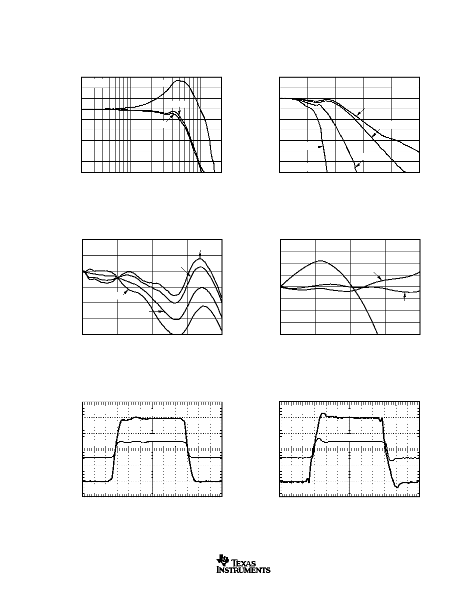
TYPICAL CHARACTERISTICS:
V
S
=
±
5V
(Cont.)
At T
A
= +25
∞
C, G = +2, and R
L
= 100
, unless otherwise specified.
-
60
-
65
-
70
-
75
-
80
-
85
-
90
-
95
-
100
Harmonic Distortion (dBc)
50
100
500
Load Resistance (
)
10MHz HARMONIC DISTORTION
vs LOAD RESISTANCE
G = +2
f = 10MHz
V
O
= 2V
PP
See Figure 1
2nd Harmonic
3rd Harmonic
-
60
-
65
-
70
-
75
-
80
-
85
-
90
-
95
-
100
Harmonic Distortion (dBc)
2.5
3.0
3.5
4.0
4.5
5.0
5.5
6.0
Supply Voltage (
±
V)
10MHz HARMONIC DISTORTION
vs SUPPLY VOLTAGE
G = +2
R
L
= 100
V
O
= 2V
PP
See Figure 1
2nd Harmonic
3rd Harmonic
-
60
-
65
-
70
-
75
-
80
-
85
-
90
-
95
-
100
Harmonic Distortion (dBc)
0.5
1
10
50
Frequency (MHz)
G = +2 HARMONIC DISTORTION vs FREQUENCY
R
L
= 100
V
O
= 2V
PP
2nd Harmonic
3rd Harmonic
See Figure 1
-
60
-
65
-
70
-
75
-
80
-
85
-
90
-
95
-
100
Harmonic Distortion (dBc)
0.5
1
5
Output Voltage (V
PP
)
10MHz HARMONIC DISTORTION
vs OUTPUT VOLTAGE
G = +2
R
L
= 100
f = 10MHz
See Figure 1
2nd Harmonic
3rd Harmonic
-
60
-
65
-
70
-
75
-
80
-
85
-
90
-
95
-
100
Harmonic Distortion (dBc)
0.5
1
10
50
Frequency (MHz)
G = +1 HARMONIC DISTORTION vs FREQUENCY
R
L
= 100
V
O
= 2V
PP
See Figure 2
2nd Harmonic
3rd Harmonic
-
50
-
55
-
60
-
65
-
70
-
75
-
80
-
85
-
90
-
95
-
100
Harmonic Distortion (dBc)
0.5
1
10
50
Frequency (MHz)
G = ≠1 HARMONIC DISTORTION vs FREQUENCY
R
L
= 100
V
O
= 2V
PP
See Figure 3
2nd Harmonic
3rd Harmonic
OPA693
9
SBOS285
www.ti.com
TYPICAL CHARACTERISTICS:
V
S
=
±
5V
(Cont.)
At T
A
= +25
∞
C, G = +2, and R
L
= 100
, unless otherwise specified.
100
10
1
Current Noise (pA/
Hz)
V
oltage Noise (nV/
Hz)
100
1k
10k
100k
1M
10M
Frequency (MHz)
INPUT VOLTAGE vs CURRENT NOISE DENSITY
22pA/
Hz
Inverting Current Noise (internal)
Noninverting Current Noise
Voltage Noise
17.8pA/
Hz
1.8nV/
Hz
60
50
40
30
20
2-TONE, 3RD-ORDER
INTERMODULATION INTERCEPT
Frequency (MHz)
0
25
50
75
100
125
150
175
200
Intercept Point (+dBm)
OPA693
50
P
I
+5V
-
5V
P
O
50
R
F
300
50
R
G
300
OPA693
P
I
+5V
-
5V
P
O
500
R
F
300
50
R
G
300
0
-
10
-
20
-
30
-
40
-
50
-
60
-
70
Return Loss (dB)
10
100
1000
Frequency (MHz)
INPUT RETURN LOSS vs FREQUENCY (S
11
)
See Figure 3
See Figure 1
VSWR < 1.2:1
G =
-
1
G = +2
0
-
10
-
20
-
30
-
40
-
50
-
60
Return Loss (dB)
10
100
1000
Frequency (MHz)
OUTPUT RETURN LOSS vs FREQUENCY (S
22
)
VSWR < 1.2:1
G = +2
See Figure 1
No Output
Trim Capacitor
With
Trim Capacitor
OPA693
50
1.8pF
S
22
60
50
40
30
20
10
0
R
S
(
)
1
10
100
Capacitive Load (pF)
RECOMMENDED R
S
vs CAPACITIVE LOAD
G = +2
< 0.1dB Peaking
OPA693
R
S
V
IN
V
O
C
L
1k
300
50
300
1k
is optional
9
6
3
0
-
3
-
6
-
9
Gain to Cap. Load (dB)
10
100
1000
Frequency (MHz)
SMALL-SIGNAL FREQUENCY RESPONSE
vs CAPACITIVE LOAD
G = +2
Optimized R
S
C
L
= 100pF
C
L
= 10pF
C
L
= 50pF
C
L
= 20pF

OPA693
10
SBOS285
www.ti.com
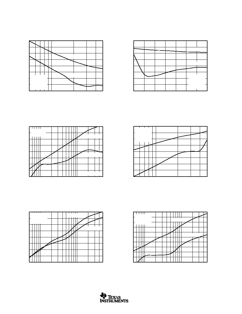
TYPICAL CHARACTERISTICS:
V
S
=
±
5V
(Cont.)
At T
A
= +25
∞
C, G = +2, and R
L
= 100
, unless otherwise specified.
65
60
55
50
45
40
35
30
25
20
Frequency (Hz)
1k
10k
100k
1M
10M
100M
PSRR vs FREQUENCY
Power-Supply Rejection Ratio (dB)
+PSRR
≠PSRR
Time (50ns/div)
INVERTING OVERDRIVE RECOVERY
Input/Output (V)
6
4
2
0
-
2
-
4
-
6
G =
-
1
R
L
= 100
See Figure 3
Input
Output
Time (50ns/div)
NONINVERTING OVERDRIVE RECOVERY
Input/Output (V)
6
4
2
0
-
2
-
4
-
6
G = +2
R
L
= 100
See Figure 1
Input
Output
150
140
130
120
110
100
15
14
13
12
11
10
SUPPLY AND OUTPUT CURRENT vs TEMPERATURE
Ambient Temperature (
∞
C)
≠50
≠25
0
25
50
75
100
125
Output Current (mA)
Supply Current (mA)
Supply Current
Right Scale
Left Scale
Sinking Output Current
Sourcing Output Current
5
4
3
2
1
0
-
1
-
2
-
3
-
4
-
5
V
O
(V)
-
250
-
200
-
150
-
100
-
50
0
250
200
150
100
50
I
O
(mA)
OUTPUT VOLTAGE AND CURRENT LIMITATIONS
1W Internal
Power
Boundary
1W Internal
Power
Boundary
100
Load Line
50
Load Line
20
Load Line
10
1
0.1
CLOSED-LOOP OUTPUT IMPEDANCE
Frequency (Hz)
10k
100M
100k
1M
10M
Output Impedance (
)
OPA693
300
+5V
≠5V
300
50
Z
O
OPA693
11
SBOS285
www.ti.com
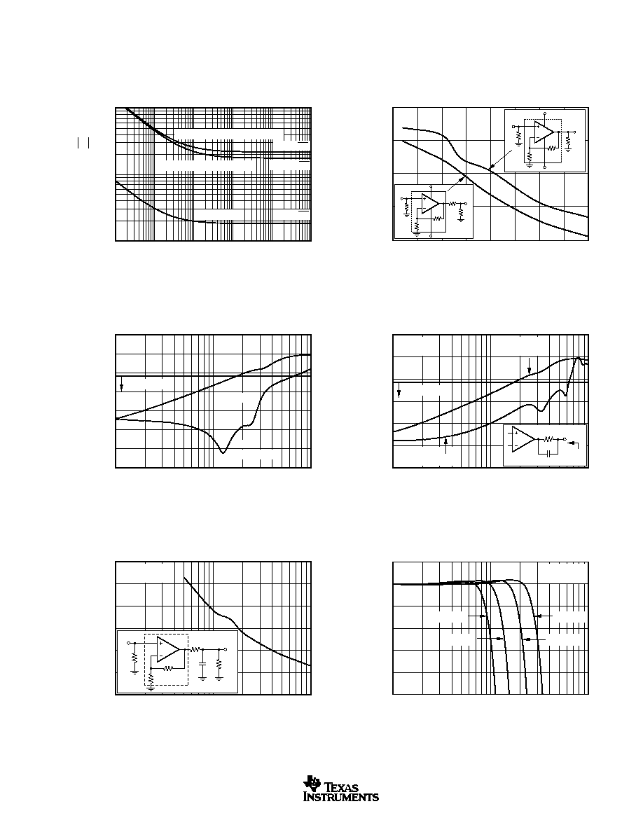
TYPICAL CHARACTERISTICS:
V
S
=
±
5V
(Cont.)
At T
A
= +25
∞
C, G = +2, and R
L
= 100
, unless otherwise specified.
Time (500ns/div)
LARGE-SIGNAL DISABLE/ENABLE RESPONSE
V
DIS
/V
OUT
(V)
7
6
5
4
3
2
1
0
-
1
-
2
-
3
G = +2
V
IN
= 1V
DC
R
L
= 100
See Figure 1
V
OUT
V
DIS
dG
0.12
0.10
0.08
0.06
0.04
0.02
0
Number of 150
Loads
1
2
3
4
COMPOSITE VIDEO dG/dP
dP
dP
dG/dP (%/
∞
)
OPA693
Video In
Video Loads
-
5V
+5V
DIS
Optional
1.0k
Pull-Down
75
No Pull-Down
With 1.0k
Pull-Down
dG
6
5
4
3
2
1
0
Input/Output Range (
±
V)
2.0
3.0
3.5
4.5
5.5
2.5
4.0
5.0
6.5
6.0
Supply Voltages (
±
V)
COMMON-MODE INPUT AND OUTPUT SWING
vs SUPPLY VOLTAGE
Input
Output
1.0
0.5
0
-
0.5
-
1.0
TYPICAL DC DRIFT OVER TEMPERATURE
Ambient Temperature (
∞
C)
≠50
≠25
0
25
50
75
100
125
Input Offset Voltage (mV)
16
8
0
-
8
-
16
Input Bias Currents (
µ
A)
V
IO
I
B
+
I
B
-
(internal)
-
20
-
30
-
40
-
50
-
60
-
70
-
80
-
90
-
100
Gain (dB)
10
100
1000
Frequency (MHz)
DISABLED FEEDTHRU vs FREQUENCY
G = +2
R
L
= 100
V
DIS
= 0V
Forward and Reverse
See Figure 1
0
4
6
2
10
12
20
14
16
18
8
Time (2ns/div)
SETTLING TIME
Input/Output (5mV/div)
20
15
10
5
0
-
5
-
10
-
15
-
20
G = +2
R
L
= 100
2V
0V
Output Step
See Figure 1
Input
Output
OPA693
12
SBOS285
www.ti.com
Time (2ns/div)
GAIN OF +1 PULSE RESPONSE
Output (V)
4.5
4.0
3.5
3.0
2.5
2.0
1.5
1.0
0.5
R
L
= 100
See Figure 5
Large Signal
Small Signal
Time (2ns/div)
GAIN OF +2 PULSE RESPONSE
Output (V)
4.5
4.0
3.5
3.0
2.5
2.0
1.5
1.0
0.5
R
L
= 100
See Figure 4
Large Signal
Small Signal
800
750
700
650
600
550
500
450
400
Small-Signal BW (MHz)
4
6
7
9
11
5
8
10
12
Single-Supply Voltage (V)
SMALL-SIGNAL BANDWIDTH
vs SINGLE-SUPPLY VOLTAGE
G = +2
V
O
= 0.5V
PP
R
L
= 100
See Figure 4
0.2
0.1
0
-
0.1
-
0.2
-
0.3
-
0.4
Normalized Gain (dB)
0
50
100
150
200
Frequency (MHz)
FREQUENCY RESPONSE FLATNESS vs LOAD
R
L
= 100
R
L
= 75
R
L
= 150
R
L
= 200
G = +2
V
O
= 1V
PP
See Figure 4
8
7
6
5
4
3
2
1
0
-
1
Gain (dB)
0
200
400
600
800
1000
Frequency (MHz)
LARGE-SIGNAL FREQUENCY RESPONSE
V
O
= 2V
PP
V
O
= 1V
PP
V
O
= 3V
PP
G = +2
R
L
= 100
See Figure 4
3
2
1
0
-
1
-
2
-
3
-
4
-
5
-
6
Normalized Gain (dB)
1
10
100
1000
Frequency (MHz)
SMALL-SIGNAL FREQUENCY RESPONSE
V
O
= 1V
PP
G =
-
1
G = +2
G = +1
TYPICAL CHARACTERISTICS:
V
S
= +5V
At T
A
= +25
∞
C, G = +2, and R
L
= 100
to V
S
/2, unless otherwise specified.
OPA693
13
SBOS285
www.ti.com
TYPICAL CHARACTERISTICS:
V
S
= +5V
(Cont.)
At T
A
= +25
∞
C, G = +2, and R
L
= 100
to V
S
/2, unless otherwise specified.
-
55
-
60
-
65
-
70
-
75
-
80
-
85
-
90
-
95
Harmonic Distortion (dBc)
0.5
1
10
50
Frequency (MHz)
HARMONIC DISTORTION vs FREQUENCY
G = +2
R
L
= 100
V
O
= 2V
PP
2nd Harmonic
3rd Harmonic
See Figure 4
-
55
-
60
-
65
-
70
-
75
-
80
-
85
-
90
-
95
Harmonic Distortion (dBc)
0.1
1
3
Output Voltage (V
PP
)
HARMONIC DISTORTION vs OUTPUT VOLTAGE
G = +2
R
L
= 100
f = 10MHz
2nd Harmonic
3rd Harmonic
See Figure 4
-
55
-
60
-
65
-
70
-
75
-
80
-
85
-
90
-
95
Harmonic Distortion (dBc)
50
100
500
Load Resistance (
)
HARMONIC DISTORTION
vs LOAD RESISTANCE
See Figure 4
G = +2
f = 10MHz
2nd Harmonic
3rd Harmonic
50
45
40
35
30
25
20
15
10
2-TONE, 3RD-ORDER
INTERMODULATION INTERCEPT
Frequency (MHz)
0
25
50
75
100
125
150
175
200
Intercept Point (+dBm)
OPA693
50
P
I
+5V
P
O
50
R
F
300
50
R
G
300
1k
1k
OPA693
P
I
+5V
P
O
500
R
F
300
50
R
G
300
1k
1k
OPA693
14
SBOS285
www.ti.com
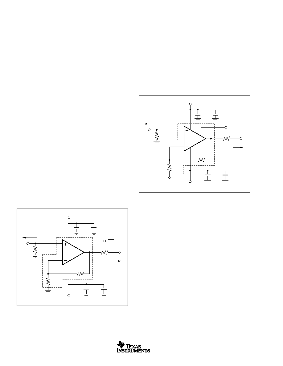
APPLICATION INFORMATION
WIDEBAND BUFFER OPERATION
The OPA693 gives the exceptional AC performance of a
wideband current-feedback op amp with a highly linear
output stage. It features internal R
F
and R
G
resistors, making
it a simple matter to select a gain of +2, +1 or ≠1 with no
external resistors. Requiring only 13mA supply current, the
OPA693's output swings to within 1V of either supply with
> 700MHz small signal bandwidth and > 300MHz delivering
7V
PP
into a 100
load. This low output headroom in a very
high-speed amplifier gives remarkable single +5V operation.
The OPA693 delivers 2V
PP
swing with > 500MHz bandwidth
operating on a single +5V supply. The primary advantage of
a current-feedback fixed gain video buffer, as opposed to a
slew-enhanced low-gain stable voltage-feedback implemen-
tation, is a higher slew rate with lower quiescent power and
output noise.
Figure 1 shows the DC-coupled, gain of +2V/V, dual power-
supply circuit configuration used as the basis for the
±
5V
Electrical Characteristics table and Typical Characteristics
curves. For test purposes, the input impedance is set to 50
with a resistor to ground and the output impedance is set to
50
with a series output resistor. Voltage swings reported in
the specifications are taken directly at the input and output
pins while load powers (dBm) are defined at a matched 50
load. For the circuit of Figure 1, the total effective load will be
100
|| 600
= 85.7
. The disable control line (DIS) is
typically left open to ensure normal amplifier operation. In
addition to the usual power supply decoupling capacitors to
ground, a 0.01
µ
F capacitor can be included between the two
power-supply pins. This optional added capacitor will typi-
cally improve the 2nd harmonic distortion performance by
3dB to 6dB.
Figure 2 shows the DC-coupled, gain of +1V/V buffer con-
figuration used as a starting point for the gain of +1V/V
Typical Characteristic curves. In this case, the inverting input
resistor, R
G
, is left open giving a very broadband gain of +1
performance. While the test circuit shows a 50
input resis-
tor, a buffer application is typically transforming from a
source that cannot drive a heavy load to a 100
load, such
as shown in Figure 2. The noninverting input impedance of
the OPA693 is typically 100k
|| 2pF. Driving directly into
the noninverting input will provide this very light load to the
source. However, the source must still provide the noninverting
input bias current required by the input stage to operate. An
alternative approach to a gain of +1 buffer is described in the
Wideband Unity Gain Buffers section of this data sheet.
OPA693
+5V
-
5V
50
Load
50
50
50
Source
R
G
300
R
F
300
+
6.8
µ
F
0.1
µ
F
+
6.8
µ
F
0.1
µ
F
V
I
V
O
DIS
Figure 1. DC-Coupled, G = +2, Bipolar-Supply, Specification
and Test Circuit.
Figure 3 shows the DC-coupled, gain of ≠1V/V buffer con-
figuration used as a starting point for the gain of ≠1V/V
Typical Characteristic curves. The input impedance is set to
50
using the parallel combination of an external 60.4
resistor and the internal 300
R
G
resistor. The noninverting
input is tied directly to ground. Since the internal design for
the OPA693 is current-feedback, trying to get improved DC
accuracy by including a resistor on the noninverting input to
ground is ineffective. Using a direct short to ground on the
noninverting input reduces both the contribution of the DC
bias current and noise current to the output error. While the
external 60.4
is used here to match to the 50
source from
the test equipment, the maximum input impedance in this
configuration is limited to the 300
R
G
resistor even with the
R
M
resistor removed. Unlike the noninverting unity gain
buffer application, removing R
M
does not strongly impact the
DC operating point because the short on the noninverting
input of Figure 3 provides the DC operating voltage. This
application of the OPA693 provides a very broadband, high-
output, signal inverter.
Figure 2. DC-Coupled, G = +1V/V, Bipolar-Supply, Specifica-
tion and Test Circuit.
OPA693
+5V
-
5V
Open
50
Load
50
50
50
Source
R
G
300
R
F
300
+
6.8
µ
F
0.1
µ
F
+
6.8
µ
F
0.1
µ
F
V
I
DIS
V
O

OPA693
15
SBOS285
www.ti.com
SINGLE-SUPPLY OPERATION
The OPA693 may be used over a single-supply range of +5V
to +12V. Though not a rail-to-rail output design, the OPA693
requires minimal input and output voltage headroom com-
pared to other very-wideband video buffer amplifiers. As
shown in the single +5V Typical Characteristic curves, the
OPA693 provides > 300MHz bandwidth driving a 3V
PP
swing
into a 100
load. The key requirement of broadband single-
supply operation is to maintain input and output signal
swings within the useable voltage ranges at both the input
and the output.
The circuit of Figure 4 shows the AC-coupled, gain of
+2V/V, video buffer circuit used as the basis for the Electrical
Characteristics table and Typical Characteristics curves. The
circuit of Figure 4 establishes an input midpoint bias using a
simple resistive divider from the +5V supply (two 604
resistors). The input signal is then AC-coupled into this
midpoint voltage bias. The input voltage can swing to within
1.7V of either supply pin, giving a 1.6V
PP
input signal range
centered between the supply pins. The input impedance
matching resistor (60.4
) used for testing is adjusted to give
a 50
input match when the parallel combination of the
biasing divider network is included. The gain resistor (R
G
) is
AC-coupled, giving the circuit a DC gain of +1, which puts the
input DC bias voltage (2.5V) on the output as well. Again, on
a single +5V supply, the output voltage can swing to within
1V of either supply pin while delivering more than 90mA
output current. A demanding 100
load to a midpoint bias is
used in this characterization circuit. The new output stage
used in the OPA693 can deliver large bipolar output current
into this midpoint load with minimal crossover distortion, as
shown by the +5V supply, 3rd-harmonic distortion plots.
While the circuit of Figure 4 shows +5V single-supply opera-
tion, this same circuit may be used for single supplies
ranging as high as +12V nominal. The noninverting input bias
resistors are relatively low in Figure 4 to minimize output DC
offset due to noninverting input bias current. At higher signal-
supply voltage, these should be increased to limit the added
supply current drawn through this path.
Figure 5 shows the AC-coupled, G = +1V/V, single-supply
specification and test circuit. In this case, the gain setting
resistor, R
G
, is simply left open to get a gain of +1V for AC
signals. Once again, the noninverting input is DC biased at
mid-supply, putting that same V
S
/2 at the output pin. The
signal is AC-coupled into this midpoint with an added termi-
nation resistor on the source side of the blocking capacitor.
Figure 3. DC-Coupled, G = ≠1V/V, Bipolar-Supply Specifica-
tion and Test Circuit.
OPA693
+5V
DIS
50
V
O
R
F
300
R
G
300
R
M
60.4
+
6.8
µ
F
0.1
µ
F
50
Load
-
5V
+
6.8
µ
F
0.1
µ
F
50
Source
V
I
Figure 4. AC-Coupled, G = +2V/V, Single-Supply Specifica-
tion and Test Circuit.
OPA693
+5V
+V
S
DIS
V
S
/2
604
100
V
O
V
I
604
R
G
300
R
F
300
1000pF
1000pF
+
6.8
µ
F
0.1
µ
F
50
Source
60.4
Figure 5. AC-Coupled, G = +1V/V, Single-Supply Specifica-
tion and Test Circuit.
OPA693
Open
V
S
/2
V
O
60.4
100
50
Source
604
604
R
G
300
R
F
300
+
6.8
µ
F
0.1
µ
F
V
I
DIS
1000pF
+5V
V
S

OPA693
16
SBOS285
www.ti.com
SINGLE-SUPPLY ADC INTERFACE
Most modern, high-performance ADCs (such as the Texas
Instruments ADS8xx series) operate on a single +5V (or
lower) power supply. It has been a considerable challenge
for single-supply op amps to deliver a low distortion input
signal at the ADC input for signal frequencies exceeding
5MHz. The high slew rate, exceptional output swing, and
high linearity of the OPA693 make it an ideal single-supply
ADC driver. Figure 6 shows an example input interface to a
very high-performance, 10-bit, 75MSPS CMOS converter.
The OPA693 in the circuit of Figure 6 provides > 500MHz
bandwidth at an operating gain of +2V/V delivering 1V
PP
at the
output for a 0.5V
PP
input. This broad bandwidth provides
adequate margin to deliver low distortion to the maximum
20Mhz analog input frequency intended for the circuit of Figure
6. A 40MHz low-pass filter is provided as part of the converter
interface to both limit broadband noise and reduce harmonics
as the signal frequency exceeds 15MHz. The noninverting input
bias voltage is referenced to the midpoint of the ADC signal
range by dividing off the top and bottom of the internal ADC
reference ladder.
WIDEBAND UNITY GAIN BUFFER WITH IMPROVED
FLATNESS
As shown in the Typical Characteristic curves, the unity gain
buffer configuration of Figure 2 shows a peaking in the fre-
quency response exceeding 2dB. This gives the slight amount
of overshoot and ringing apparent in the gain of +1V/V pulse
response curves. A similar circuit that holds a flatter frequency
response, giving improved pulse fidelity, is shown in Figure 7.
This circuit removes the peaking by bootstrapping out any
parasitic effects on R
G
. The input impedance is still set by R
M
as the apparent impedance looking into R
G
is very high. R
M
may be increased to show a higher input impedance, but
larger values will start to impact DC output offset voltage.
Figure 6. Wideband, AC-Coupled, Single-Supply ADC Driver.
OPA693
300
+2.5V DC Bias
ADS828
10-Bit
75MSPS
50
1V
PP
DIS
100pF
Input
300
REFB
REFT
CM
Input
1000pF
1000pF
0.5V
PP
2k
0.1
µ
F
+3.5V
2k
0.1
µ
F
+1.5V
+5V
Clock
+5V
R
G
R
F
Figure 7. Improved Unity Gain Buffer.
OPA693
+5V
DIS
R
O
50
V
O
R
F
300
R
G
300
R
M
50
-
5V
V
I
Figure 8. Buffer Frequency Response Comparison.
2
1
0
-
1
-
2
-
3
-
4
-
5
-
6
Normalized Gain (dB)
10
100
1000
Frequency (MHz)
G = +1, Figure 2
G = +1, Figure 7
This circuit creates an additional input offset voltage as the
difference in the two input bias currents times the impedance
to ground at V
I
. Figure 8 shows a comparison of small-signal
frequency response for the unity gain buffer of Figure 2
compared to the improved approach shown in Figure 7.
OPA693
17
SBOS285
www.ti.com
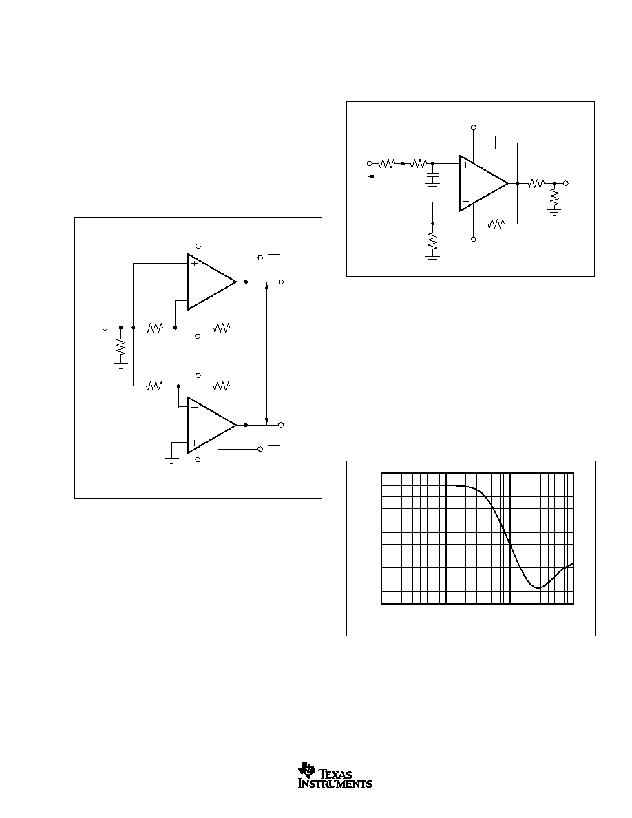
WIDEBAND, DC-COUPLED,
SINGLE-TO-DIFFERENTIAL CONVERSION
The frequency response shown in Figure 7 for the improved
gain of +1V/V buffer closely matches the inverting gain of
≠1V/V frequency response. Combining two OPA693s to give
a +1 and ≠1 response will give a very broadband, DC-
coupled, single-ended input to differential output conversion.
Figure 9 shows this implementation where the input match is
now set by R
M
in parallel with the R
G
resistor of the inverting
stage. This circuit is essentially providing a DC to 700MHz
1:1 transformer operation. A 50
input match is shown, but
this may be increased by increasing R
M
. For instance,
targeting a 200
input impedance requires an R
M
= 600
to
get the parallel combination of R
M
and R
G
= 200
.
Figure 9. DC
700MHz, Single-to-Differential Conversion.
OPA693
+5V
DIS
DIS
+V
I
R
F
300
R
G
300
R
M
60.4
-
5V
V
I
OPA693
+5V
-
V
I
2V
I
R
F
300
R
G
300
-
5V
HIGH-FREQUENCY ACTIVE FILTERS
The extremely wide bandwidth of the OPA693 allows a wide
range of active filter topologies to be implemented with
minimal amplifier bandwidth interaction in the filter shape.
Sallen-Key filters, using either a gain of 1 or gain of 2
amplifier, may be easily implemented with no external gain
setting elements. In general, given a desired filter W
O
, the
amplifier should have at least 20X that W
O
to minimize filter
interaction with the amplifier frequency response. Figure 10
Figure 10. Line Driver with 40 MHz Low-Pass Active Filter.
OPA693
+5V
-
5V
50
50
22pF
226
100
0
Source
R
G
300
R
F
300
22pF
V
I
V
O
This type of filter depends on a low output impedance from
the amplifier through very high frequencies to continue to
provide an increasing attenuation with frequency. As the
amplifier output impedance rises with frequency, any input
signal or noise starts to feed directly through to the output via
the feedback capacitor. Since the OPA693 used in Figure 10
has a 700MHz bandwidth, the active filter will continue to roll
off through frequencies exceeding 200MHz. Figure 11 shows
the frequency response for the filter of Figure 10, where the
desired 40MHz cutoff is achieved and a 40dB/dec rolloff is
held through very high frequencies.
Figure 11. 40MHz Low-Pass Active Filter Response.
3
0
-
3
-
6
-
9
-
12
-
15
-
18
-
21
-
24
-
27
-
30
Gain (dB)
1
10
100
1000
Frequency (MHz)
shows an example gain of +2 line driver using the OPA693
that incorporates a 40MHz low-pass Butterworth response
with just a few external components. The filter resistor values
have been adjusted slightly here from an ideal filter analysis
to account for parasitic effects.

OPA693
18
SBOS285
www.ti.com
DESIGN-IN TOOLS
DEMONSTRATION BOARDS
Two printed circuit (PC) boards are available to assist in the
initial evaluation of the circuit performance using the OPA693 in
its two package styles. Both are available free as unpopulated
PC boards delivered with descriptive documentation. The sum-
mary information for these boards is shown in Table I.
either the output capabilities or the 1W dissipation limit. A
100
load line (the standard test-circuit load) shows full
±
3.8V output swing capability, as shown in the Typical
Characteristics.
The minimum specified output voltage and current specifica-
tions over temperature are set by worst-case simulations at
the cold temperature extreme. Only at cold startup will the
output current and voltage decrease to the numbers shown
in the over-temperature min/max specifications. As the out-
put transistors deliver power, their junction temperatures
increase, which decreases their V
BE
's (increasing the avail-
able output voltage swing) and increases their current gains
(increasing the available output current). In steady state
operation, the available output voltage and current will al-
ways be greater than that shown in the over-temperature
characteristics since the output stage junction temperatures
will be higher than the minimum specified operating ambient.
To maintain maximum output stage linearity, no output short-
circuit protection is provided. This will not normally be a
problem, since most applications include a series matching
resistor at the output that limits the internal power dissipation
if the output side of this resistor is shorted to ground.
However, shorting the output pin directly to an adjacent
positive power supply pin will, in most cases, destroy the
amplifier. If additional protection to a power-supply short is
required, consider a small series resistor in the power supply
leads. Under heavy output loads, this will reduce the avail-
able output voltage swing. A 5
series resistor in each
supply lead will limit the internal power dissipation to < 1W for
an output short while decreasing the available output voltage
swing only 0.5V, for up to 100mA desired load currents.
Always place the 0.1
µ
F power supply decoupling capacitors
after these supply current limiting resistors directly on the
device supply pins.
DRIVING CAPACITIVE LOADS
One of the most demanding, and yet very common, load
conditions for an op amp is capacitive loading. Often, the
capacitive load is the input of an ADC, including additional
external capacitance, which may be recommended to improve
ADC linearity. A high-speed, high open-loop gain, amplifier like
the OPA693 can be very susceptible to decreased stability
and may give closed-loop response peaking when a capaci-
tive load is placed directly on the output pin. When the
amplifier's open loop output resistance is considered, this
capacitive load introduces an additional pole in the signal path
that can decrease the phase margin. Several external solu-
tions to this problem have been suggested. When the primary
considerations are frequency response flatness, pulse re-
sponse fidelity and/or distortion, the simplest and most effec-
tive solution is to isolate the capacitive load from the feedback
loop by inserting a series isolation resistor between the ampli-
fier output and the capacitive load. This does not eliminate the
pole from the loop response, but rather shifts it and adds a
zero at a higher frequency. The additional zero acts to cancel
the phase lag from the capacitive load pole, thus increasing
the phase margin and improving stability.
To request either of these boards, check the Texas Instru-
ments web site at www.ti.com.
OPERATING SUGGESTIONS
GAIN SETTING
Setting the gain for the OPA693 is very easy. For a gain of +2,
ground the ≠IN pin and drive the +IN pin with the signal. For
a gain of +1, either leave the ≠IN pin open and drive the +IN
pin or drive both the +IN and ≠IN pins as shown in Figure 7.
For a gain of ≠1, ground the +IN pin and drive the ≠IN pin with
the input signal. An external resistor may be used in series
with the ≠IN pin to reduce the gain. However, since the internal
resistors (R
F
and R
G
) have a tolerance and temperature drift
different than the external resistor, the absolute gain accuracy
and gain drift over temperature will be relatively poor com-
pared to the previously described standard gain connections
using no external resistor.
OUTPUT CURRENT AND VOLTAGE
The OPA693 provides output voltage and current capabilities
that can easily support multiple video loads and/or 100
loads with very low distortion. Under no-load conditions at
25
∞
C, the output voltage typically swings to 1V of either
supply rail; the tested swing limit is within 1.2V of either rail.
Into a 15
load (the minimum tested load), it is tested to
deliver more than
±
90mA.
The specifications described above, though familiar in the
industry, consider voltage and current limits separately. In
many applications, it is the voltage
◊
current, or V-I product,
which is more relevant to circuit operation. Refer to the
Output Voltage and Current Limitations plot in the Typical
Characteristics. The X and Y axes of this graph show the
zero-voltage output current limit and the zero-current output
voltage limit, respectively. The four quadrants give a more
detailed view of the OPA693's output drive capabilities,
noting that the graph is bounded by a "Safe Operating Area"
of 1W maximum internal power dissipation. Superimposing
resistor load lines onto the plot shows that the OPA693 can
drive
±
3.4V into 20
or
±
3.7V into 50
without exceeding
DEMO BOARD
LITERATURE
PART
REQUEST
PRODUCT
PACKAGE
NUMBER
NUMBER
OPA693ID
SO-8
DEM-OPA68xU
SBOU009
OPA693IDBV
SOT23-6
DEM-OPA6xxN
SBOU010
TABLE I. Demo Board Ordering Information.
OPA693
19
SBOS285
www.ti.com
The Typical Characteristics show a Recommended R
S
vs
Capacitive Load curve to help the designer pick a value to
give < 0.1dB peaking to the load. The resulting frequency
response curves show a 0.1dB peaked response for several
selected capacitive loads and recommended R
S
combina-
tions. Parasitic capacitive loads greater than 2pF can begin
to degrade the performance of the OPA693. Long PC board
traces, unmatched cables, and connections to other amplifier
inputs can easily exceed this value. Always consider this
effect carefully, and add the recommended series resistor as
close as possible to the OPA693 output pin (see the Board
Layout Guidelines section).
The criterion for setting this R
S
resistor is a maximum
bandwidth, flat frequency response at the load (< 0.1dB
peaking). For the OPA693 operating in a gain of +2, the
frequency response at the output pin is very flat to begin with,
allowing relatively small values of R
S
to be used for low
capacitive loads.
DISTORTION PERFORMANCE
The OPA693 provides good distortion performance into a
100
load on
±
5V supplies. Relative to alternative solutions,
the OPA693 holds much lower distortion at higher frequencies
(> 20Mhz) than alternative solutions. Generally, until the
fundamental signal reaches very high frequency or power
levels, the 2nd harmonic will dominate the distortion with a
negligible 3rd harmonic component. Focusing then on the 2nd
harmonic, increasing the load impedance improves distortion
directly. Remember that the total load includes the feedback
network--in the noninverting configuration (see Figure 1) this
is the sum of R
F
+ R
G
, while in the inverting configuration it is
just R
F
(see Figure 3). Also, providing an additional supply de-
coupling capacitor (0.01
µ
F) between the supply pins (for
bipolar operation) improves the 2nd-order distortion slightly
(3dB to 6dB).
The OPA693 has an extremely low 3rd-order harmonic
distortion. This also produces a high 2-tone, 3rd-order inter-
modulation intercept. Two graphs for this intercept are given
in the in the Typical Characteristics; one for
±
5V and one for
+5V. The lower curve shown in each graph is defined at the
50
load when driven through a 50
matching resistor, to
allow direct comparisons to RF MMIC devices. The higher
curve in each graph shows the intercept if the output is taken
directly at the output pin with a 500
load, to allow prediction
of the 3rd-order spurious level when driving a lighter load,
such as an ADC input. The output matching resistor attenu-
ates the voltage swing from the output pin to the load by 6dB.
If the OPA693 drives directly into the input of a high-
impedance device, such as an ADC, this 6dB attenuation is
not taken and the intercept will increase a minimum of 6dB,
as shown in the 500
load typical characteristic.
The intercept is used to predict the intermodulation spurious
levels for two closely-spaced frequencies. If the two test fre-
quencies (f1 and f2) are specified in terms of average and delta
frequency, f
O
= (f1 + f2)/2 and
f = |f2 ≠ f1|/2, then the two, 3rd-
order, close-in spurious tones will appear at f
O
±
3
◊
f. The
difference between two equal test tone power levels and these
intermodulation spurious power levels is given by
dBc = 2
◊
(IM3 ≠ P
O
), where IM3 is the intercept taken from
the Typical Characteristics and P
O
is the power level in dBm at
the 50
load for one of the two closely-spaced test frequencies.
For instance, at 50MHz, the OPA693 at a gain of +2 has an
intercept of 44dBm at a matched 50
load. If the full envelope
of the two frequencies needs to be 2V
PP
at this load, this
requires each tone to be 4dBm (1V
PP
). The 3rd-order inter-
modulation spurious tones will then be 2
◊
(44 ≠ 4) = 80dBc
below the test tone power level (≠76dBm). If this same 2V
PP
2-tone envelope were delivered directly into a lighter 500
load,
the intercept would increase to the 52dBm shown in the Typical
Characteristics. With the same output signal and gain condi-
tions, but now driving directly into a light load with no matching
loss, the 3rd-order spurious tones will then be at least
2
◊
(52 ≠ 4) = 96dBc below the 4dBm test tone power levels
centered on 50MHz (≠92dBm). We are still using a 4dBm for the
1V
PP
output swing into this 500
load. While not strictly correct
from a power standpoint, this does give the correct prediction for
spurious level. The class AB output stage for the OPA693 is
much more voltage swing dependent on output distortion than
strictly power dependent. To use the 500
intercept curve, use
the single-tone voltage swing as if it were driving a 50
load to
compute the P
O
used in the intercept equation.
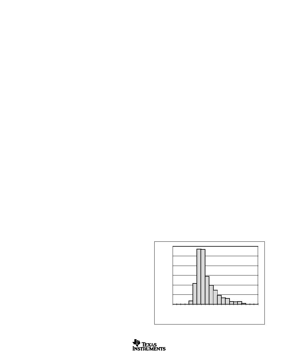
GAIN ACCURACY AND LINEARITY
The OPA693 provides improved absolute gain accuracy and
DC linearity over earlier fixed gain of two line drivers. Oper-
ating at a gain of +2V/V by tying the ≠IN pin to ground, the
OPA693 shows a maximum gain error of
±
0.9% at 25
∞
C. The
DC gain will therefore lie between 1.982V/V and 2.018V/V at
room temperature. Over the specified temperature ranges,
this gain tolerance expands only slightly due to the matched
temperature drift for R
F
and R
G
. Achieving this gain accuracy
requires a very low impedance ground at ≠IN. Typical pro-
duction lots show a much tighter distribution in gain than this
±
0.9% specification. Figure 12 shows a typical distribution in
measured gain at the gain of +2V/V configuration, in this
case showing a slight drop in the mean (0.25%) from the
nominal but with a very tight distribution.
Figure 12. Typical +2V/V Gain Distribution.
Gain(V/V)
Mean = 1.995
= 0.005
Number of Units
600
500
400
300
200
100
0
1.980
1.982
1.984
1.986
1.988
1.990
1.992
1.994
1.996
1.998
2.000
2.002
2.004
2.006
2.008
2.010
2.012
2.014
2.016
2.018
2.020
OPA693
20
SBOS285
www.ti.com
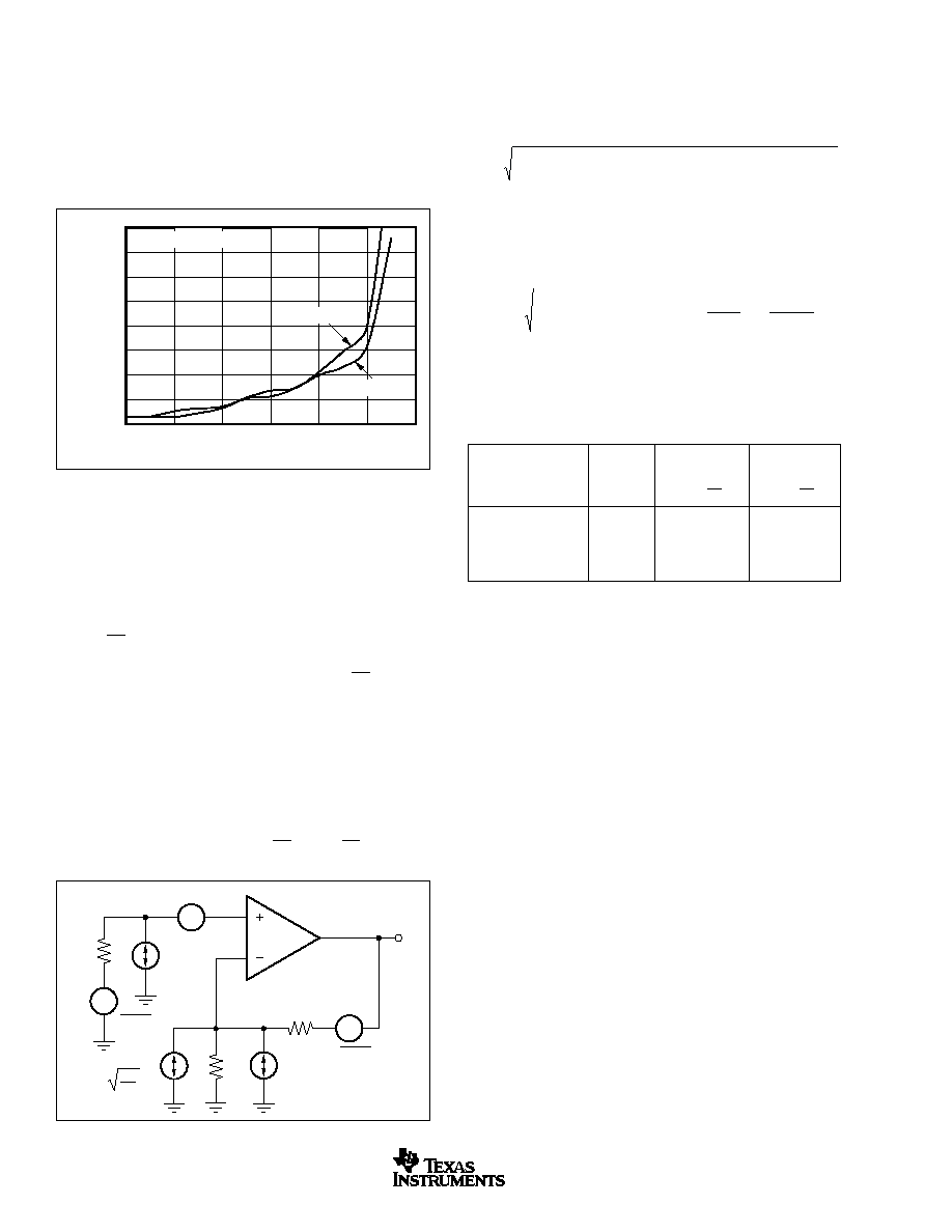
The exceptionally linear output stage (as illustrated by the
high 3rd-order intermodulation intercept) and low thermal
gradient induced errors for the OPA693 give an extremely
linear output over large voltage swings and heavy loads.
Figure 13 shows the tested deviation (in % of peak to peak)
from linearity for a range of symmetrical output swings and
loads. Below 4V
PP
, for either a 100
or a 500
load, the
OPA693 delivers > 14-bit linear output response.
The total output spot noise voltage can be computed as the
square root of the sum of all squared output noise voltage
contributors. Equation 1 shows the general form for the
output noise voltage using the terms shown in Figure 14.
(1)
E
E
I
R
kTR
NG
I R
kTR NG
O
NI
BN S
S
BI F
F
=
+
(
)
+
+
(
)
+
2
2
2
2
4
4
Dividing this expression through by noise gain (NG = 1 + R
F
/R
G
)
will give the equivalent input-referred spot noise voltage at the
non-inverting input, as shown in Equation 2.
(2)
E
E
I
R
kTR
I R
NG
kTR
NG
N
NI
BN S
S
BI F
F
=
+
(
)
+
+
+
2
2
2
4
4
Evaluating the output noise and input noise expressions for
the two noninverting gain configurations, and with two differ-
ent values for the noninverting source impedance, gives
output and input referred spot noise voltages of Table II.
OUTPUT
TOTAL INPUT
SPOT NOISE
SPOT NOISE
R
S
E
O
E
N
CONFIGURATION
(
)
(nV/
Hz )
(nV/
Hz )
G = +2 (Figure 1)
25
8.3
4.15
G = +2 (Figure 1)
300
14
7
G = +1 (Figure 2)
25
7.3
7.3
G = +1 (Figure 2)
300
9.2
9.2
TABLE II. Total Output and Input Referred Noise.
4kT
R
G
R
G
R
F
R
S
OPA693
I
BI
E
O
I
BN
4kT = 1.6E ≠20J
at 290
∞
K
E
RS
E
NI
4kTR
S
4kTR
F
Figure 14. Op Amp Noise Model.
The output noise is being dominated by the inverting current
noise times the internal feedback resistor. This gives a total
input referred noise voltage that exceeds the 1.8nV voltage
term for the amplifier itself.
DC ACCURACY AND OFFSET CONTROL
A current-feedback op amp like the OPA693 provides excep-
tional bandwidth and slew rate giving fast pulse settling but
only moderate DC accuracy. The Electrical Characteristics
show an input offset voltage comparable to high-speed volt-
age-feedback amplifiers. However, the two input bias currents
are somewhat higher and are unmatched. Whereas bias
current cancellation techniques are very effective with most
voltage-feedback op amps, they do not generally reduce the
output DC offset for wideband current-feedback op amps.
Since the two input bias currents are unrelated in both mag-
nitude and polarity, matching the source impedance looking
out of each input to reduce their error contribution to the output
is ineffective. Evaluating the configuration of Figure 1, using
worst case +25
∞
C input offset voltage and the two input bias
currents, gives a worst-case output offset range equal to:
±
(NG
◊
V
OS
) + (I
BN
◊
R
S
/2
◊
NG)
±
(I
BI
◊
R
F
)
=
±
(2
◊
2.0mV)
±
(35
µ
A
◊
25
◊
2)
±
(50
µ
A
◊
300
)
=
±
4mV
±
1.75mV
±
15mV
=
±
30.75mV
where NG = noninverting signal gain.
Figure 13. DC Linearity vs Output Swing and Loads.
0.0200
0.0175
0.0150
0.0125
0.0100
0.0075
0.0050
0.0025
0
V
O
(peak to peak)
2
3
4
5
6
7
8
% Deviation
Figure 1 Test Circuit
R
L
= 100
R
L
= 500
NOISE PERFORMANCE
The OPA693 offers an excellent balance between voltage and
current noise terms to achieve a low output noise under a
variety of operating conditions. The inverting node noise
current (internal) will appear at the output multiplied by the
relatively low 300
feedback resistor. The input noise voltage
(1.8nV/
Hz) is extremely low for a unity gain stable amplifier.
This low input voltage noise was achieved at the price of
higher noninverting input current noise (17.8pA/
Hz). As long
as the AC source impedance looking out of the noninverting
input is less than 100
, this current noise will not contribute
significantly to the total output noise. The op amp input voltage
noise and the two input current noise terms combine to give
low output noise for the each of the three gain settings
available using the OPA693. Figure 14 shows the op amp
noise analysis model with all of the noise terms included. In
this model, all noise terms are taken to be noise voltage or
current density terms in either nV/
Hz or pA/
Hz.

OPA693
21
SBOS285
www.ti.com
Minimizing the resistance seen by the noninverting input will
minimize the output DC error. For improved DC precision in
a wideband low-gain amplifier, consider the OPA842 where
a bipolar input is acceptable (low source resistance) or the
OPA656 where a JFET input is required.
DISABLE OPERATION
The OPA693 provides an optional disable feature that can be
used to reduce system power. If the V
DIS
control pin is left
unconnected, the OPA693 will operate normally. This shut-
down is intended only as a power-savings feature. Forward
path isolation when disabled is very good for small signals for
gains of +1 or +2. Large-signal isolation is not ensured. Using
this feature to multiplex two or more outputs together is not
recommended. Large signals applied to the disabled output
stages can turn on parasitic devices degrading signal linear-
ity for the desired channel.
Turn-on time is very quick from the shutdown condition,
typically < 60ns. Turn-off time is strongly dependent on the
selected gain configuration and load, but is typically 3
µ
s for
the circuit of Figure 1.
To shutdown, the control pin must be asserted low. This logic
control is referenced to the positive supply, as shown in the
simplified circuit of Figure 15.
The shutdown feature for the OPA693 is a positive supply
referenced, current-controlled, interface. Open collector (or
drain) interfaces are most effective, as long as the controlling
logic can sustain the resulting voltage (in the open mode)
that will appear at the V
DIS
pin. That voltage will be one diode
below the positive supply voltage applied to the OPA693. For
voltage output logic interfaces, the on/off voltage levels
described in the Electrical Characteristics apply only for a
+5V positive supply on the OPA693. An open-drain interface
is recommended for shutdown operation using a higher
positive supply for the OPA693 and/or logic families with
inadequate high-level voltage swings.
THERMAL ANALYSIS
The OPA693 does not require heatsinking or airflow in most
applications. Maximum desired junction temperature sets the
maximum allowed internal power dissipation as described
here. In no case should the maximum junction temperature
be allowed to exceed 150
∞
C.
Operating junction temperature (T
J
) is given by T
A
+ P
D
◊
JA
.
The total internal power dissipation (P
D
) is the sum of
quiescent power (P
DQ
) and additional power dissipated in the
output stage (P
DL
) to deliver load power. Quiescent power is
simply the specified no-load supply current times the total
supply voltage across the part. P
DL
will depend on the
required output signal and load but would, for a grounded
resistive load, be at a maximum when the output is fixed at
a voltage equal to 1/2 either supply voltage (for equal bipolar
supplies). Under this worst-case condition, P
DL
= V
S
2
/(4
◊
R
L
)
where R
L
includes feedback network loading. This is the
absolute highest power that can be dissipated for a given R
L
.
All actual applications will dissipate less power in the output
stage.
Note that it is the power in the output stage and not into the
load that determines internal power dissipation.
As a worst-case example, compute the maximum T
J
using an
OPA693IDBV (SOT23-6 package) in the circuit of Figure 1
operating at the maximum specified ambient temperature of
+85
∞
C and driving a grounded 100
load. Maximum internal
power is:
P
D
= 10V
◊
14.1mA + 5
2
/(4
◊
(100
+|| 600
)) = 214mW
Maximum T
J
= +85
∞
C + (0.21W
◊
150
∞
C/W) = 117
∞
C.
All actual applications will operate at a lower junction tem-
perature than the 117
∞
C computed above. Compute your
actual output stage power to get an accurate estimate of
maximum junction temperature, or use the results shown
here as an absolute maximum.
25k
110k
15k
I
S
Control
≠V
S
+V
S
V
DIS
Q1
Figure 15. Simplified Disable Control Circuit.
In normal operation, base current to Q1 is provided through
the 110k
resistor while the emitter current through the 15k
resistor sets up a voltage drop that is inadequate to turn on
the two diodes in Q1's emitter. As V
DIS
is pulled LOW,
additional current is pulled through the 15k
, eventually
turning on these two diodes (
80
µ
A). At this point, any further
current pulled out of V
DIS
goes through those diodes holding
the emitter-base voltage of Q1 at approximately 0V. This
shuts off the collector current out of Q1, turning the amplifier
off. The supply current in the shutdown mode is only that
required to operate the circuit of Figure 15.

OPA693
22
SBOS285
www.ti.com
BOARD LAYOUT GUIDELINES
Achieving optimum performance with a high-frequency amplifier
like the OPA693 requires careful attention to PC board layout
parasitics and external component types. Recommendations
that will optimize performance include:
a) Minimize parasitic capacitance to any AC ground for all
of the signal I/O pins. Parasitic capacitance on the output can
cause instability; on the noninverting input, it can react with the
source impedance to cause unintentional bandlimiting. To
reduce unwanted capacitance, create a window around the
signal I/O pins in all of the ground and power planes around
those pins. Otherwise, ground and power planes should be
unbroken elsewhere on the board.
b) Minimize the distance (< 0.25") from the power supply pins
to high frequency 0.1
µ
F decoupling capacitors. At the device
pins, the ground and power plane layout should not be in close
proximity to the signal I/O pins. Avoid narrow power and ground
traces to minimize inductance between the pins and the decou-
pling capacitors. The power supply connections should always
be decoupled with these capacitors. Larger (2.2
µ
F to 6.8
µ
F)
decoupling capacitors, effective at lower frequency, should also
be used on the supply pins. These may be placed somewhat
farther from the device and may be shared among several
devices in the same area of the PC board.
c) Careful selection and placement of external compo-
nents will preserve the high frequency performance of the
OPA693. Use resistors that have low reactance at high
frequencies. Surface-mount resistors work best and allow a
tighter overall layout. Metal film and carbon composition axi-
ally-leaded resistors can also provide good high-frequency
performance. Again, keep their leads and PC board trace
length as short as possible. Never use wirewound type resis-
tors in a high-frequency application. Since the output pin and
inverting input pin are the most sensitive to parasitic capaci-
tance, always position the series output resistor, if any, as
close as possible to the output pin. Since the inverting input
node is internal for the OPA693, it is more robust to layout
issues than amplifiers with similar speed but external feedback
and gain resistors. Other network components, such as
noninverting input termination resistors, should also be placed
close to the package. Good axial metal film or surface mount
resistors have approximately 0.2pF in shunt with the resistor.
For resistor values > 2.0k
, this parasitic capacitance can add
a pole and/or zero below 400MHz that can effect circuit
operation. Keep resistor values as low as possible consistent
with load driving considerations.
d) Connections to other wideband devices on the PC board
may be made with short direct traces or through onboard
transmission lines. For short connections, consider the trace
and the input to the next device as a lumped capacitive load.
Relatively wide traces (50 to 100mils) should be used, prefer-
ably with ground and power planes opened up around them.
Estimate the total capacitive load and set R
S
from the plot of
Recommended R
S
vs Capacitive Load. Low parasitic capacitive
loads (< 4pF) may not need an R
S
since the OPA693 is
nominally compensated to operate with a 2pF parasitic load. If
a long trace is required, and the 6dB signal loss intrinsic to a
doubly-terminated transmission line is acceptable, implement a
matched impedance transmission line using microstrip or stripline
techniques (consult an ECL design handbook for microstrip and
stripline layout techniques). A 50
environment is normally not
necessary on board, and in fact, a higher impedance environ-
ment will improve distortion, as shown in the distortion versus
load plots. With a characteristic board trace impedance defined
based on board material and trace dimensions, a matching
series resistor into the trace from the output of the OPA693 is
used, as well as a terminating shunt resistor at the input of the
destination device. Remember also that the terminating imped-
ance will be the parallel combination of the shunt resistor and
the input impedance of the destination device; this total effective
impedance should be set to match the trace impedance. If the
6dB attenuation of a doubly-terminated transmission line is
unacceptable, a long trace can be series-terminated at the
source end only. Treat the trace as a capacitive load in this case
and set the series resistor value as shown in the plot of
Recommended R
S
vs Capacitive Load. This will not preserve
signal integrity as well as a doubly-terminated line. If the input
impedance of the destination device is low, there will be some
signal attenuation due to the voltage divider formed by the
series output into the terminating impedance.
e) Socketing a high-speed part like the OPA693 is not
recommended. The additional lead length and pin-to-pin
capacitance introduced by the socket can create an extremely
troublesome parasitic network, which can make it almost
impossible to achieve a smooth, stable frequency response.
Best results are obtained by soldering the OPA693 directly
onto the board.
INPUT AND ESD PROTECTION
The OPA693 is built using a very high-speed complementary
bipolar process. The internal junction breakdown voltages are
relatively low for these very small geometry devices. These
breakdowns are reflected in the Absolute Maximum Ratings
table. All device pins are protected with internal ESD protec-
tion diodes to the power supplies, as shown in Figure 16.
These diodes provide moderate protection to input overdrive
voltages above the supplies as well. The protection diodes can
typically support 30mA continuous current. Where higher
currents are possible (for example, in systems with
±
15V
supply parts driving into the OPA693), current limiting series
resistors may be added on the noninverting input. Keep this
resistor value as low as possible since high values degrade
both noise performance and frequency response. The invert-
ing input already has a 300
resistor from the external pin to
the internal summing junction for the op amp. This provides
considerable protection for that node.
Figure 16. Internal ESD Protection.
External
Pin
+V
CC
≠V
CC
Internal
Circuitry
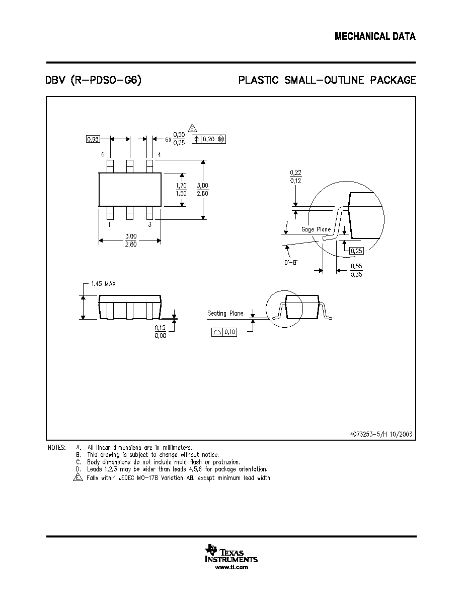
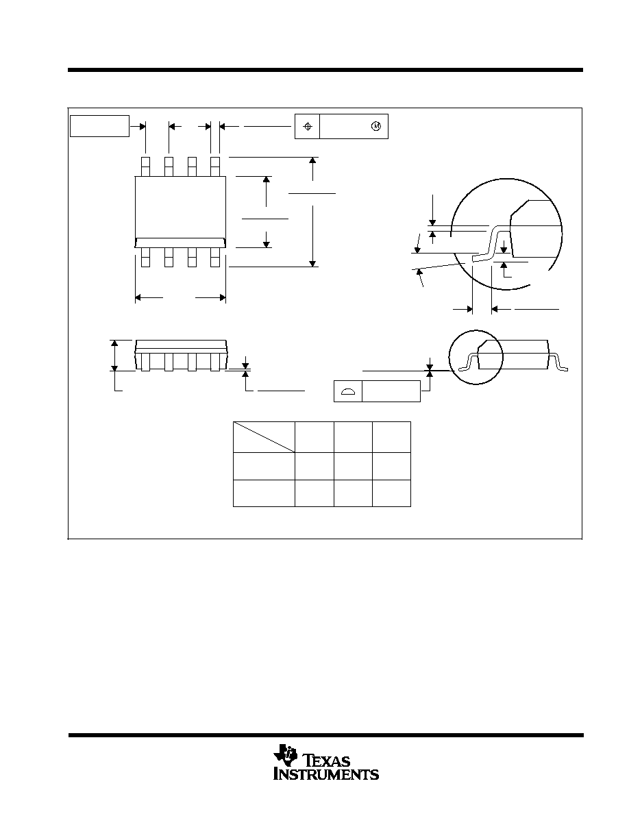
MECHANICAL DATA
MSOI002B ≠ JANUARY 1995 ≠ REVISED SEPTEMBER 2001
POST OFFICE BOX 655303
∑
DALLAS, TEXAS 75265
D (R-PDSO-G**)
PLASTIC SMALL-OUTLINE PACKAGE
8 PINS SHOWN
8
0.197
(5,00)
A MAX
A MIN
(4,80)
0.189
0.337
(8,55)
(8,75)
0.344
14
0.386
(9,80)
(10,00)
0.394
16
DIM
PINS **
4040047/E 09/01
0.069 (1,75) MAX
Seating Plane
0.004 (0,10)
0.010 (0,25)
0.010 (0,25)
0.016 (0,40)
0.044 (1,12)
0.244 (6,20)
0.228 (5,80)
0.020 (0,51)
0.014 (0,35)
1
4
8
5
0.150 (3,81)
0.157 (4,00)
0.008 (0,20) NOM
0
∞
≠ 8
∞
Gage Plane
A
0.004 (0,10)
0.010 (0,25)
0.050 (1,27)
NOTES: A. All linear dimensions are in inches (millimeters).
B. This drawing is subject to change without notice.
C. Body dimensions do not include mold flash or protrusion, not to exceed 0.006 (0,15).
D. Falls within JEDEC MS-012

IMPORTANT NOTICE
Texas Instruments Incorporated and its subsidiaries (TI) reserve the right to make corrections, modifications,
enhancements, improvements, and other changes to its products and services at any time and to discontinue
any product or service without notice. Customers should obtain the latest relevant information before placing
orders and should verify that such information is current and complete. All products are sold subject to TI's terms
and conditions of sale supplied at the time of order acknowledgment.
TI warrants performance of its hardware products to the specifications applicable at the time of sale in
accordance with TI's standard warranty. Testing and other quality control techniques are used to the extent TI
deems necessary to support this warranty. Except where mandated by government requirements, testing of all
parameters of each product is not necessarily performed.
TI assumes no liability for applications assistance or customer product design. Customers are responsible for
their products and applications using TI components. To minimize the risks associated with customer products
and applications, customers should provide adequate design and operating safeguards.
TI does not warrant or represent that any license, either express or implied, is granted under any TI patent right,
copyright, mask work right, or other TI intellectual property right relating to any combination, machine, or process
in which TI products or services are used. Information published by TI regarding third-party products or services
does not constitute a license from TI to use such products or services or a warranty or endorsement thereof.
Use of such information may require a license from a third party under the patents or other intellectual property
of the third party, or a license from TI under the patents or other intellectual property of TI.
Reproduction of information in TI data books or data sheets is permissible only if reproduction is without
alteration and is accompanied by all associated warranties, conditions, limitations, and notices. Reproduction
of this information with alteration is an unfair and deceptive business practice. TI is not responsible or liable for
such altered documentation.
Resale of TI products or services with statements different from or beyond the parameters stated by TI for that
product or service voids all express and any implied warranties for the associated TI product or service and
is an unfair and deceptive business practice. TI is not responsible or liable for any such statements.
Following are URLs where you can obtain information on other Texas Instruments products and application
solutions:
Products
Applications
Amplifiers
amplifier.ti.com
Audio
www.ti.com/audio
Data Converters
dataconverter.ti.com
Automotive
www.ti.com/automotive
DSP
dsp.ti.com
Broadband
www.ti.com/broadband
Interface
interface.ti.com
Digital Control
www.ti.com/digitalcontrol
Logic
logic.ti.com
Military
www.ti.com/military
Power Mgmt
power.ti.com
Optical Networking
www.ti.com/opticalnetwork
Microcontrollers
microcontroller.ti.com
Security
www.ti.com/security
Telephony
www.ti.com/telephony
Video & Imaging
www.ti.com/video
Wireless
www.ti.com/wireless
Mailing Address:
Texas Instruments
Post Office Box 655303 Dallas, Texas 75265
Copyright
2003, Texas Instruments Incorporated