Document Outline
- FEATURES
- APPLICATIONS
- DESCRIPTION
- RELATED PRODUCTS
- ABSOLUTE MAXIMUM RATINGS(1)
- PACKAGE/ORDERING INFORMATION(1)
- PIN CONFIGURATIONS
- ELECTRICAL CHARACTERISTICS: VS = ±5V
- ELECTRICAL CHARACTERISTICS: VS = +3.3V
- TYPICAL CHARACTERISTICS: VS = ±5V
- TYPICAL CHARACTERISTICS: VS = + 5V
- TYPICAL CHARACTERISTICS: VS = + 3.3V
- APPLICATIONS INFORMATION
- WIDEBAND VOLTAGE-FEEDBACK OPERATION
- DESIGN-IN TOOLS
- DEMONSTRATION BOARDS
- MACROMODEL AND APPLICATIONS SUPPORT
- GAIN OF +2V/V VIDEO LINE DRIVER
- SINGLE-SUPPLY ADC INTERFACE
- UNITY-GAIN BUFFER
- OPERATING SUGGESTIONS
- GAIN SETTING
- OUTPUT CURRENT AND VOLTAGES
- DRIVING CAPACITIVE LOADS
- DISTORTION PERFORMANCE
- NOISE PERFORMANCE
- DC ACCURACY AND OFFSET CONTROL
- THERMAL ANALYSIS
- BOARD LAYOUT GUIDELINES
- PACKAGE OPTION ADDENDUM
- MECHANICAL DATA
- DBV (R-PDSO-G5) PLASTIC SMALL-OUTLINE PACKAGE
- D (R-PDSO-G8) PLASTIC SMALL-OUTLINE PACKAGE

FEATURES
D
HIGH BANDWIDTH: 80MHz (G = +2)
D
LOW SUPPLY CURRENT: 3.9mA
D
FLEXIBLE SUPPLY RANGE:
+2.8V to +11V Single Supply
±
1.4V to
±
5.5V Dual Supply
D
INPUT RANGE INCLUDES GROUND ON
SINGLE SUPPLY
D
4.9V
PP
OUTPUT SWING ON +5V SUPPLY
D
HIGH SLEW RATE: 350V/
µ
sec
D
LOW INPUT VOLTAGE NOISE: 9.3nV/
Hz
D
AVAILABLE IN AN SOT23 PACKAGE
APPLICATIONS
D
SINGLE-SUPPLY VIDEO LINE DRIVERS
D
CCD IMAGING CHANNELS
D
LOW-POWER ULTRASOUND
D
PORTABLE CONSUMER ELECTRONICS
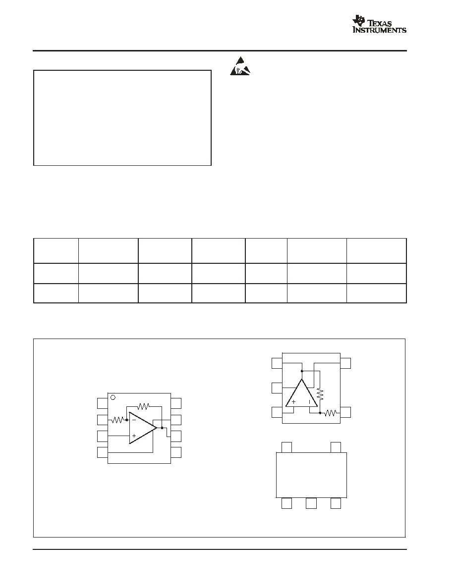
DESCRIPTION
The OPA832 is a low-power, high-speed, fixed-gain amplifier
designed to operate on a single +3.3V or +5V supply.
Operation on
±
5V or +10V supplies is also supported. The
input range extends below ground and to within 1V of the
positive supply. Using complementary common-emitter
outputs provides an output swing to within 30mV of ground
and 130mV of the positive supply. The high output drive
current and low differential gain and phase errors also make
it ideal for single-supply consumer video products.
Low distortion operation is ensured by the high gain
bandwidth product (200MHz) and slew rate (850V/
µ
s), making
the OPA832 an ideal input buffer stage to 3V and 5V CMOS
converters. Unlike other low-power, single-supply amplifiers,
distortion performance improves as the signal swing is
decreased. A low 9.3nV/
Hz input voltage noise supports
wide dynamic range operation.
The OPA832 is available in an industry-standard SO-8
package. The OPA832 is also available in an ultra-small
SOT23-5 package. For gains other than +1, -1, or +2,
consider using the OPA830.
RELATED PRODUCTS
DESCRIPTION
SINGLES
DUALS
TRIPLES
QUADS
Medium Speed
OPA830
OPA2830
--
OPA4830
Medium Speed,
Fixed Gain
--
OPA2832
OPA3832
--
OPA832
+3.3V
80.6
75
400
400
V
O
75
Load
V
I
V
O
= 1V/V
I
I
976
Video DAC
V
I
Single-Supply, Low-Cost Video Line Driver
0
-
3
-
6
-
9
Ga
i
n
(
d
B
)
Frequency (MHz)
1
10
100
LARGE-SIGNAL BANDWIDTH
(1V
PP
AT MATCHED LOAD)
OPA832
SBOS266B - JUNE 2003 - REVISED SEPTEMBER 2004
Low-Power, Single-Supply, Fixed-Gain
Video Buffer Amplifier
PRODUCTION DATA information is current as of publication date. Products
conform to specifications per the terms of Texas Instruments standard warranty.
Production processing does not necessarily include testing of all parameters.
www.ti.com
Copyright
2003-2004, Texas Instruments Incorporated
Please be aware that an important notice concerning availability, standard warranty, and use in critical applications of Texas Instruments
semiconductor products and disclaimers thereto appears at the end of this data sheet.
All trademarks are the property of their respective owners.
OPA832
SBOS266B - JUNE 2003 - REVISED SEPTEMBER 2004
www.ti.com
2
ABSOLUTE MAXIMUM RATINGS
(1)
Power Supply
+12VDC
. . . . . . . . . . . . . . . . . . . . . . . . . . . . . . . . . . . .
Internal Power Dissipation
See Thermal Characteristics
. . . . . . . . .
Differential Input Voltage(2)
±
1.2V
. . . . . . . . . . . . . . . . . . . . . . . . . . .
Input Voltage Range
-0.5V to +VS + 0.3V
. . . . . . . . . . . . . . . . . . . . .
Storage Temperature Range: D, DBV
-40
∞
C to +125
∞
C
. . . . . . . . .
Lead Temperature (soldering, 10s)
+300
∞
C
. . . . . . . . . . . . . . . . . . . .
Junction Temperature (TJ)
+150
∞
C
. . . . . . . . . . . . . . . . . . . . . . . . . . .
ESD Rating:
Human Body Model (HBM)
2000V
. . . . . . . . . . . . . . . . . . . . . . .
Charge Device Model (CDM)
1500V
. . . . . . . . . . . . . . . . . . . . .
Machine Model (MM)
200V
. . . . . . . . . . . . . . . . . . . . . . . . . . . . . .
(1) Stresses above these ratings may cause permanent damage.
Exposure to absolute maximum conditions for extended periods
may degrade device reliability. These are stress ratings only, and
functional operation of the device at these or any other conditions
beyond those specified is not supported.
(2) Noninverting input to internal inverting node.
This integrated circuit can be damaged by ESD. Texas
Instruments recommends that all integrated circuits be
handled with appropriate precautions. Failure to observe
proper handling and installation procedures can cause damage.
ESD damage can range from subtle performance degradation to
complete device failure. Precision integrated circuits may be more
susceptible to damage because very small parametric changes could
cause the device not to meet its published specifications.
PACKAGE/ORDERING INFORMATION
(1)
PRODUCT
PACKAGE-LEAD
PACKAGE
DESIGNATOR
SPECIFIED
TEMPERATURE
RANGE
PACKAGE
MARKING
ORDERING
NUMBER
TRANSPORT
MEDIA, QUANTITY
OPA832
SO-8 Surface-Mount
D
-40
∞
C to +85
∞
C
OPA832
OPA832ID
Rails, 100
OPA832IDR
Tape and Reel, 2500
OPA832
SOT23-5
DBV
-40
∞
C to +85
∞
C
A74
OPA832IDBVT
Tape and Reel, 250
OPA832IDBVR
Tape and Reel, 3000
(1) For the most current package and ordering information, see the Package Option Addendum located at the end of this data sheet.
PIN CONFIGURATIONS
1
2
3
5
4
Output
-
V
S
Noninverting Input
+V
S
Inverting Input
A74
1
2
3
5
4
Pin Orientation/Package Marking
SOT23-5
400
400
1
2
3
4
8
7
6
5
NC
Inverting Input
Noninverting Input
-
V
S
NC
+V
S
Output
NC
SO-8
NC = No Connection
400
400

OPA832
SBOS266B - JUNE 2003 - REVISED SEPTEMBER 2004
www.ti.com
3
ELECTRICAL CHARACTERISTICS: V
S
=
±
5V
Boldface limits are tested at +25
∞
C.
At TA = 25
∞
C, G = +2, and RL = 150
to GND, unless otherwise noted (see Figure 3).
OPA832ID, IDBV
TYP
MIN/MAX OVER TEMPERATURE
PARAMETER
CONDITIONS
+25
∞
C
+25
∞
C(1)
0
∞
C to
70
∞
C(2)
-40
∞
C to
+85
∞
C(2)
UNITS
MIN/
MAX
TEST
LEVEL(3)
AC PERFORMANCE (see Figure 3)
Small-Signal Bandwidth
G = +2, VO
0.5VPP
80
55
54
54
MHz
min
B
G = -1, VO
0.5VPP
99
57
56
56
MHz
min
B
Peaking at a Gain of +1
VO
0.5VPP
4.2
dB
typ
C
Slew Rate
G = +2, 2V Step
350
230
230
220
V/
µ
s
min
B
Rise Time
0.5V Step
4.6
ns
max
B
Fall Time
0.5V Step
4.9
ns
max
B
Settling Time to 0.1%
G = +2, 1V Step
45
ns
max
B
Harmonic Distortion
VO = 2VPP, 5MHz
2nd-Harmonic
RL = 150
-64
-60
-60
-60
dBc
max
B
RL = 500
-66
-63
-63
-63
dBc
max
B
3rd-Harmonic
RL = 150
-57
-50
-49
-48
dBc
max
B
RL = 500
-73
-64
-61
-57
dBc
max
B
Input Voltage Noise
f > 1MHz
9.2
nV/
Hz
max
B
Input Current Noise
f > 1MHz
2.2
pA/
Hz
max
B
NTSC Differential Gain
RL = 150
0.10
%
typ
C
NTSC Differential Phase
RL = 150
0.16
∞
typ
C
DC PERFORMANCE(4)
Gain Error
G = +2
±
0.3
±
1.5
±
1.6
±
1.7
%
min
A
G = -1
±
0.2
±
1.5
±
1.6
±
1.7
%
max
B
Internal RF and RG
Maximum
400
455
460
462
max
A
Minimum
400
345
340
338
max
A
Average Drift
±
0.1
±
0.1
%/
∞
C
max
B
Input Offset Voltage
±
1.4
±
7
±
8
±
8.5
mV
max
A
Average Offset Voltage Drift
--
±
20
±
20
µ
V/
∞
C
max
B
Input Bias Current
+5.5
+10
+12
+13
µ
A
max
A
Input Bias Current Drift
±
12
±
12
nA/
∞
C
max
B
Input Offset Current
±
0.1
±
1.5
±
2
±
2.5
µ
A
max
A
Input Offset Current Drift
--
±
10
±
10
nA/
∞
C
max
B
INPUT
Negative Input Voltage Range
-5.4
-5.2
-5.0
-4.9
V
max
B
Positive Input Voltage Range
3.2
3.1
3.0
2.9
V
min
A
Input Impedance
Differential Mode
10
2.1
k
pF
typ
C
Common-Mode
400
1.2
k
pF
typ
C
OUTPUT
Output Voltage Swing
RL = 1k
to GND
±
4.9
±
4.8
±
4.75
±
4.75
V
max
A
RL = 150
to GND
±
4.6
±
4.5
±
4.45
±
4.4
V
max
A
Current Output, Sinking
85
65
60
55
mA
min
A
Current Output, Sourcing
85
65
60
55
mA
min
A
Short-Circuit Current
Output Shorted to Either Supply
120
mA
typ
C
Closed-Loop Output Impedance
G = +2, f
100kHz
0.2
typ
C
POWER SUPPLY
Minimum Operating Voltage
±
1.4
V
min
B
Maximum Operating Voltage
--
±
5.5
±
5.5
±
5.5
V
max
A
Maximum Quiescent Current
VS =
±
5V
4.25
4.7
5.3
5.9
mA
max
A
Minimum Quiescent Current
VS =
±
5V
4.25
4.0
3.6
3.3
mA
min
A
Power-Supply Rejection Ratio (PSRR)
Input-Referred
68
63
62
61
dB
min
A
THERMAL CHARACTERISTICS
Specification: ID, IDBV
-40 to +85
∞
C
typ
C
Thermal Resistance
D
SO-8
125
∞
C/W
typ
C
DBV SOT23-5
150
∞
C/W
typ
C
(1) Junction temperature = ambient for +25
∞
C specifications.
(2) Junction temperature = ambient at low temperature limits; junction temperature = ambient +5
∞
C at high temperature limit for over temperature specifications.
(3) Test levels: (A) 100% tested at +25
∞
C. Over temperature limits by characterization and simulation. (B) Limits set by characterization and simulation. (C) Typical
value only for information.
(4) Current is considered positive out of node.

OPA832
SBOS266B - JUNE 2003 - REVISED SEPTEMBER 2004
www.ti.com
4
ELECTRICAL CHARACTERISTICS: V
S
= +5V
Boldface limits are tested at +25
∞
C.
At TA = 25
∞
C, G = +2, and RL = 150
to VCM = 2V, unless otherwise noted (see Figure 1).
OPA832ID, IDBV
TYP
MIN/MAX OVER TEMPERATURE
PARAMETER
CONDITIONS
+25
∞
C
+25
∞
C
(1)
0
∞
C to
70
∞
C
(2)
-40
∞
C to
+85
∞
C
(2)
UNITS
MIN/
MAX
TEST
LEVEL
(3)
AC PERFORMANCE (see Figure 1)
Small-Signal Bandwidth
G = +2, V
O
0.5V
PP
92
56
55
55
MHz
min
B
G = -1, V
O
0.5V
PP
103
60
58
58
MHz
min
B
Peaking at a Gain of +1
V
O
0.5V
PP
4.2
dB
typ
C
Slew Rate
G = +2, 2V Step
348
230
223
223
V/
µ
s
min
B
Rise Time
0.5V Step
4.3
ns
max
B
Fall Time
0.5V Step
4.6
ns
max
B
Settling Time to 0.1%
G = +2, 1V Step
4.6
ns
max
B
Harmonic Distortion
V
O
= 2V
PP
, 5MHz
2nd-Harmonic
R
L
= 150
-59
-56
-56
-55
dBc
max
B
R
L
= 500
-62
-59
-59
-59
dBc
max
B
3rd-Harmonic
R
L
= 150
-56
-50
-49
-47
dBc
max
B
R
L
= 500
-72
-65
-62
-58
dBc
max
B
Input Voltage Noise
f > 1MHz
9.3
nV/
Hz
max
B
Input Current Noise
f > 1MHz
2.3
pA/
Hz
max
B
NTSC Differential Gain
R
L
= 150
0.11
%
typ
C
NTSC Differential Phase
R
L
= 150
0.14
∞
typ
C
DC PERFORMANCE
(4)
Gain Error
G = +2
±
0.3
±
1.5
±
1.6
±
1.7
%
min
A
G = -1
±
0.2
±
1.5
±
1.6
±
1.7
%
max
B
Internal R
F
and R
G
, Maximum
400
455
460
462
max
A
Minimum
400
345
340
338
max
A
Average Drift
0.1
0.1
%/
∞
C
max
B
Input Offset Voltage
±
0.5
±
5
±
6
±
6.5
mV
max
A
Average Offset Voltage Drift
--
±
20
±
20
µ
V/
∞
C
max
B
Input Bias Current
V
CM
= 2.0V
5.5
+10
+12
+13
µ
A
max
A
Input Bias Current Drift
±
12
±
12
nA/
∞
C
max
B
Input Offset Current
V
CM
= 2.0V
±
0.1
±
1.5
±
2
±
2.5
µ
A
max
A
Input Offset Current Drift
--
±
10
±
10
nA/
∞
C
max
B
INPUT
Least Positive Input Voltage
-0.5
-0.2
0
+0.1
V
max
B
Most Positive Input Voltage
3.3
3.2
3.1
3.0
V
min
B
Input Impedance
Differential-Mode
10
2.1
k
pF
typ
C
Common-Mode
400
1.2
k
pF
typ
C
OUTPUT
Least Positive Output Voltage
R
L
= 1k
to 2.0V
0.03
0.16
0.18
0.20
V
max
A
R
L
= 150
to 2.0V
0.18
0.3
0.35
0.40
V
max
A
Most Positive Output Voltage
R
L
= 1k
to 2.0V
4.94
4.8
4.6
4.4
V
min
A
R
L
= 150
to 2.0V
4.86
4.6
4.5
4.4
V
min
A
Current Output, Sourcing
80
60
55
52
mA
min
A
Current Output, Sinking
80
60
55
52
mA
min
A
Short-Circuit Output Current
Output Shorted to Either Supply
100
mA
typ
C
Closed-Loop Output Impedance
G = +2, f
100kHz
0.2
typ
C
POWER SUPPLY
Minimum Operating Voltage
+2.8
V
typ
C
Maximum Operating Voltage
--
+11
+11
+11
V
max
A
Maximum Quiescent Current
V
S
= +5V
3.9
4.1
4.8
5.5
mA
max
A
Minimum Quiescent Current
V
S
= +5V
3.9
3.7
3.5
3.2
mA
min
A
Power-Supply Rejection Ratio (PSRR)
Input-Referred
66
61
60
59
dB
min
A
THERMAL CHARACTERISTICS
Specification: ID, IDBV
-40 to +85
∞
C
typ
C
Thermal Resistance
D
SO-8
125
∞
C/W
typ
C
DBV SOT23-5
150
∞
C/W
typ
C
(1)
Junction temperature = ambient for +25
∞
C specifications.
(2)
Junction temperature = ambient at low temperature limits; junction temperature = ambient +5
∞
C at high temperature limit for over temperature.
(3)
Test levels: (A) 100% tested at +25
∞
C. Over temperature limits by characterization and simulation. (B) Limits set by characterization and simulation. (C) Typical value only
for information.
(4) Current is considered positive out of node.
OPA832
SBOS266B - JUNE 2003 - REVISED SEPTEMBER 2004
www.ti.com
5
ELECTRICAL CHARACTERISTICS: V
S
= +3.3V
Boldface limits are tested at +25
∞
C.
At TA = 25
∞
C, G = +2, and RL = 150
to VCM = 0.75V, unless otherwise noted (see Figure 2).
OPA832ID, IDBV
TYP
MIN/MAX OVER
TEMPERATURE
PARAMETER
CONDITIONS
+25
∞
C
+25
∞
C(1)
0
∞
C to
70
∞
C(2)
UNITS
MIN/
MAX
TEST
LEVEL(3)
AC PERFORMANCE (see Figure 2)
Small-Signal Bandwidth
G = +2, VO
0.5VPP
95
59
57
MHz
min
B
G = -1, VO
0.5VPP
103
63
61
MHz
min
B
Peaking at a Gain of +1
VO
0.5VPP
4.2
dB
typ
C
Slew Rate
1V Step
170
115
115
V/
µ
s
min
B
Rise Time
0.5V Step
4
ns
max
B
Fall Time
0.5V Step
4.2
ns
max
B
Settling Time to 0.1%
1V Step
48
ns
max
B
Harmonic Distortion
5MHz
2nd-Harmonic
RL = 150
-71
-64
-62
dBc
max
B
RL = 500
-74
-70
-66
dBc
max
B
3rd-Harmonic
RL = 150
-66
-60
-55
dBc
max
B
RL = 500
-69
-66
-62
dBc
max
B
Input Voltage Noise
f > 1MHz
9.4
nV/
Hz
max
B
Input Current Noise
f > 1MHz
2.4
pA/
Hz
max
B
DC PERFORMANCE(4)
Gain Error
G = +2
±
0.3
±
1.5
±
1.6
%
min
A
G = -1
±
0.2
±
1.5
±
1.6
%
max
B
Internal RF and RG
Maximum
400
455
460
max
A
Minimum
400
345
340
max
A
Average Drift
0.1
%/
∞
C
max
B
Input Offset Voltage
±
1
±
7
±
8
mV
max
A
Average Offset Voltage Drift
--
±
20
µ
V/
∞
C
max
B
Input Bias Current
VCM = 0.75V
5.5
+10
+12
µ
A
max
A
Input Bias Current Drift
±
12
nA/
∞
C
max
B
Input Offset Current
VCM = 0.75V
±
0.1
±
1.5
±
2
µ
A
max
A
Input Offset Current Drift
--
±
10
nA/
∞
C
max
B
INPUT
Least Positive Input Voltage
-0.5
-0.3
-0.2
V
max
B
Most Positive Input Voltage
1.5
1.4
1.3
V
min
B
Input Impedance, Differential-Mode
10
2.1
k
pF
typ
C
Common-Mode
400
1.2
k
pF
typ
C
OUTPUT
Least Positive Output Voltage
RL = 1k
to 0.75V
0.03
0.16
0.18
V
max
B
RL = 150
to 0.75V
0.1
0.3
0.35
V
max
B
Most Positive Output Voltage
RL = 1k
to 0.75V
3
2.8
2.6
V
min
B
RL = 150
to 0.75V
3
2.8
2.6
V
min
B
Current Output, Sourcing
35
25
20
mA
min
A
Current Output, Sinking
35
25
20
mA
min
A
Short-Circuit Output Current
Output Shorted to Either Supply
80
mA
typ
C
Closed-Loop Output Impedance
See Figure 2, f < 100kHz
0.2
typ
C
POWER SUPPLY
Minimum Operating Voltage
+2.8
V
typ
C
Maximum Operating Voltage
--
+11
+11
V
max
A
Maximum Quiescent Current
VS = +3.3V
3.8
4.0
4.7
mA
max
A
Minimum Quiescent Current
VS = +3.3V
3.8
3.4
3.2
mA
min
A
Power-Supply Rejection Ratio (PSRR)
Input-Referred
60
dB
typ
C
THERMAL CHARACTERISTICS
Specification: ID, IDBV
-40 to +85
∞
C
typ
C
Thermal Resistance
D
SO-8
125
∞
C/W
typ
C
DBV SOT23-5
150
∞
C/W
typ
C
(1)
Junction temperature = ambient for +25
∞
C specifications.
(2)
Junction temperature = ambient at low temperature limits; junction temperature = ambient +5
∞
C at high temperature limit for over temperature.
(3)
Test levels: (A) 100% tested at +25
∞
C. Over temperature limits by characterization and simulation. (B) Limits set by characterization and simulation. (C) Typical value only
for information.
(4) Current is considered positive out of node.
OPA832
SBOS266B - JUNE 2003 - REVISED SEPTEMBER 2004
www.ti.com
6
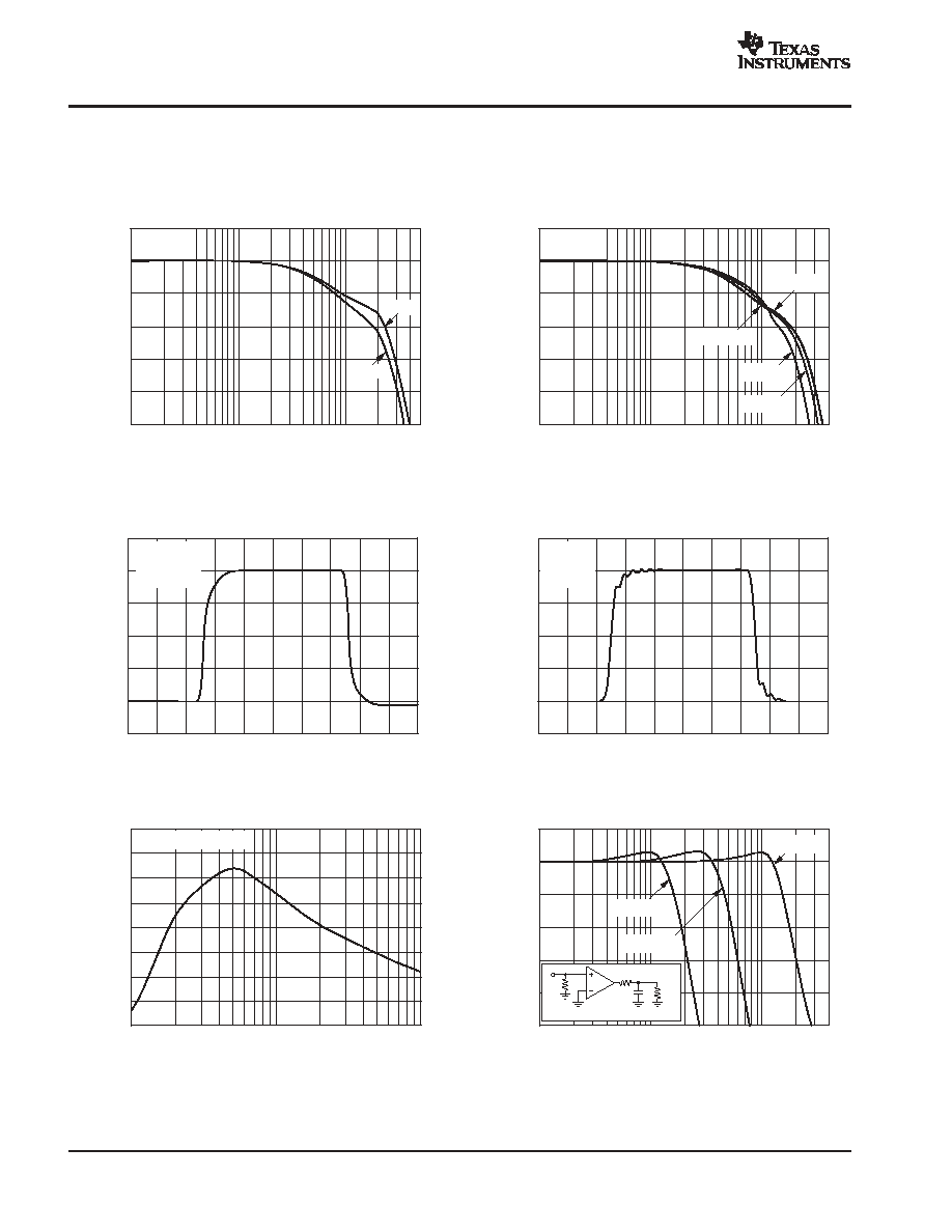
TYPICAL CHARACTERISTICS: V
S
=
±
5V
At TA = 25
∞
C, G = +2, and RL = 150
to GND, unless otherwise noted (see Figure 3).
3
0
-
3
-
6
-
9
-
12
-
15
SMALL-SIGNAL FREQUENCY RESPONSE
Frequency (MHz)
N
o
r
m
a
l
iz
e
d
G
a
in
(
d
B
)
1
10
100
500
V
O
= 0.2V
PP
R
L
= 150
G =
-
1
G = +2
150
100
50
0
-
50
-
100
-
150
SMALL-SIGNAL PULSE RESPONSE
Time (10ns/div)
O
u
t
p
u
t
V
o
l
t
ag
e
(
50
mV
/
d
i
v
)
G = +2V/V
R
L
= 150
V
O
= 0.2V
PP
40
35
30
25
20
15
10
5
0
REQUIRED R
S
vs CAPACITIVE LOAD
Capacitive Load (pF)
R
S
(
)
10
100
1k
1dB Peaking Targeted
3
0
-
3
-
6
-
9
-
12
-
15
LARGE-SIGNAL FREQUENCY RESPONSE
Frequency (MHz)
N
o
r
m
a
l
iz
e
d
G
a
in
(
d
B
)
1
10
100
400
R
L
= 150
G = +2V/V
V
O
= 0.5V
PP
V
O
= 1V
PP
V
O
= 2V
PP
V
O
= 4V
PP
1.5
1.0
0.5
0
-
0.5
-
1.0
-
1.5
LARGE-SIGNAL PULSE RESPONSE
Time (10ns/div)
O
u
tput
V
o
l
t
age
(
500
mV
/d
i
v
)
G = +2V/V
R
L
= 150
V
O
= 2V
PP
3
0
-
3
-
6
-
9
-
12
-
15
FREQUENCY RESPONSE vs CAPACITIVE LOAD
Frequency (MHz)
N
o
r
m
al
i
z
ed
G
a
i
n
t
o
C
apac
i
t
i
v
e
L
o
a
d
(
dB
)
1
10
100
400
C
L
= 1000pF
C
L
= 100pF
C
L
= 10pF
1k
(1)
C
L
R
S
V
I
NOTE: (1) 1k
is optional.
OPA832
OPA832
SBOS266B - JUNE 2003 - REVISED SEPTEMBER 2004
www.ti.com
7
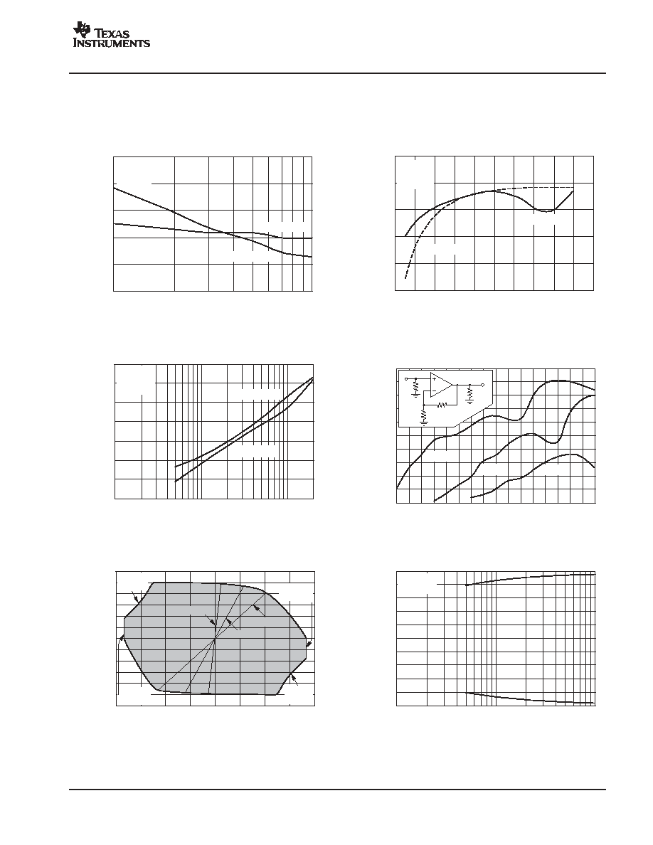
TYPICAL CHARACTERISTICS: V
S
=
±
5V (continued)
At TA = 25
∞
C, G = +2, and RL = 150
to GND, unless otherwise noted (see Figure 3).
-
40
-
50
-
60
-
70
-
80
-
90
HARMONIC DISTORTION vs LOAD RESISTANCE
Load Resistance (
)
H
a
r
m
on
i
c
D
i
s
t
or
ti
o
n
(
d
B
c
)
100
1k
G = +2V/V
V
O
= 2V
PP
f = 5MHz
3rd-Harmonic
2nd-Harmonic
-
40
-
50
-
60
-
70
-
80
-
90
-
100
-
110
HARMONIC DISTORTION vs FREQUENCY
Frequency (MHz)
Ha
r
m
o
n
i
c
Di
s
t
o
r
ti
o
n
(
d
B
c
)
0.1
1
10
20
3rd-Harmonic
2nd-Harmonic
G = +2V/V
R
L
= 500
V
O
= 2V
PP
6
5
4
3
2
1
0
-
1
-
2
-
3
-
4
-
5
-
6
OUTPUT VOLTAGE AND CURRENT LIMITATIONS
I
O
(mA)
V
O
(V
)
-
160
-
120
-
80
-
40
0
40
80
120
160
1W In ternal
Pow er Limit
Output
C urrent Limit
Output
Current Lim it
1W Internal
P ower Limit
R
L
= 500
R
L
= 100
R
L
= 50
-
50
-
60
-
70
-
80
-
90
-
100
HARMONIC DISTORTION vs OUTPUT VOLTAGE
Output Swing (V
PP
)
H
a
r
m
on
i
c
D
i
s
t
or
ti
o
n
(
d
B
c
)
0
1
2
3
4
5
6
7
8
9
10
3rd-Harmonic
G = +2V/V
R
L
= 500
f = 5MHz
2nd-Harmonic
-
40
-
45
-
50
-
55
-
60
-
65
-
70
-
75
-
80
-
85
-
90
TWO-TONE, 3RD-ORDER
INTERMODULATION SPURIOUS
Single-Tone Load Power (2dBm/div)
3r
d
-
O
r
d
e
r
S
pu
r
i
ous
Lev
el
(
d
B
c
)
-
26
-
22
-
18
-
14
-
10
-
6
-
2
2
6
10MHz
5MHz
20MHz
400
P
I
P
O
50
500
400
OPA832
5
4
3
2
1
0
-
1
-
2
-
3
-
4
-
5
OUTPUT SWING vs LOAD RESISTANCE
R
L
(
)
M
a
x
i
m
u
m
O
utp
u
t
V
ol
ta
ge
(
V
)
10
100
1k
G = +2V/V
V
S
=
±
5V

OPA832
SBOS266B - JUNE 2003 - REVISED SEPTEMBER 2004
www.ti.com
8
TYPICAL CHARACTERISTICS: V
S
= +5V
At TA = 25
∞
C, G = +2, and RL = 150
to VCM = 2V, unless otherwise noted (see Figure 1).
3
0
-
3
-
6
-
9
-
12
-
15
SMALL-SIGNAL FREQUENCY RESPONSE
Frequency (MHz)
N
o
r
m
a
l
iz
e
d
G
a
in
(
d
B
)
1
10
100
400
G =
-
1
G = +2
V
O
= 0.2V
PP
R
L
= 150
0.15
0.10
0.05
0
-
0.05
-
0.10
-
0.15
SMALL-SIGNAL PULSE RESPONSE
Time (10ns/div)
O
u
t
p
u
t
V
o
l
t
ag
e
(
50
mV
/
d
i
v
)
G = +2V/V
R
L
= 150
V
O
= 0.2V
PP
40
35
30
25
20
15
10
5
0
REQUIRED R
S
vs CAPACITIVE LOAD
Capacitive Load (pF)
R
S
(
)
10
100
1k
1dB Peaking Targeted
3
0
-
3
-
6
-
9
-
12
-
15
LARGE-SIGNAL FREQUENCY RESPONSE
Frequency (MHz)
N
o
r
m
a
l
iz
e
d
G
a
in
(
d
B
)
1
10
100
400
V
O
= 2V
PP
V
O
= 1V
PP
V
O
= 0.5V
PP
R
L
= 150
G = +2V
PP
1.5
1.0
0.5
0
-
0.5
-
1.0
-
1.5
LARGE-SIGNAL PULSE RESPONSE
Time (10ns/div)
O
u
tput
V
o
l
t
age
(
500
mV
/d
i
v
)
G = +2V/V
R
L
= 150
V
O
= 2V
PP
3
0
-
3
-
6
-
9
-
12
-
15
-
18
FREQUENCY RESPONSE vs CAPACITIVE LOAD
Frequency (MHz)
N
o
r
m
al
i
z
ed
G
a
i
n
t
o
C
apac
i
t
i
v
e
L
o
a
d
(
dB
)
1
10
100
300
C
L
= 1000pF
C
L
= 100pF
C
L
= 10pF
R
S
1k
(1)
V
I
C
L
NOTE: (1) 1k
is optional.
OPA832
SBOS266B - JUNE 2003 - REVISED SEPTEMBER 2004
www.ti.com
9
TYPICAL CHARACTERISTICS: V
S
= +5V (continued)
At TA = 25
∞
C, G = +2, and RL = 150
to VCM = 2V, unless otherwise noted (see Figure 1).
-
40
-
50
-
60
-
70
-
80
-
90
HARMONIC DISTORTION vs LOAD RESISTANCE
Load Resistance (
)
H
a
r
m
on
i
c
D
i
s
t
or
ti
o
n
(
d
B
c
)
100
1k
G = +2V/V
V
O
= 2V
PP
f = 5MHz
3rd-Harmonic
2nd-Harmonic
-
40
-
50
-
60
-
70
-
80
-
90
-
100
HARMONIC DISTORTION vs OUTPUT VOLTAGE
Output Voltage Swing (V
PP
)
H
a
r
m
on
i
c
D
i
s
t
or
ti
o
n
(
d
B
c
)
0.5
1.0
1.5
2.0
2.5
3.0
3.5
4.0
4.5
3rd-Harmonic
G = +2V/V
R
L
= 500
f = 5MHz
2nd-Harmonic
-
40
-
45
-
50
-
55
-
60
-
65
-
70
-
75
-
80
-
85
-
90
TWO-TONE, 3RD-ORDER
INTERMODULATION SPURIOUS
Single-Tone Load Power (dBm)
3r
d-
O
r
de
r
S
pu
r
i
ou
s
L
ev
el
(
d
B
c
)
-
24
-
22
-
20
-
18
-
16
-
14
-
12
-
10
-
8
-
6
-
4
-
2
10MHz
5MHz
20MHz
OPA832
P
I
P
O
50
500
-
40
-
50
-
60
-
70
-
80
-
90
-
100
-
110
G = +2, HARMONIC DISTORTION vs FREQUENCY
Frequency (MHz)
H
a
r
m
on
i
c
D
i
s
t
or
ti
o
n
(
d
B
c
)
0.1
1
10
20
3rd-Harmonic
2nd-Harmonic
G = +2V/V
R
L
= 500
V
O
= 2V
PP
-
30
-
40
-
50
-
60
-
70
-
80
-
90
-
100
-
110
G =
-
1, HARMONIC DISTORTION vs FREQUENCY
Frequency (MHz)
H
a
r
m
on
i
c
D
i
s
t
or
ti
o
n
(
d
B
c
)
0.1
1
10
20
3rd-Harmonic
2nd-Harmonic
G =
-
1V/V
R
L
= 500
f = 5MHz
100
10
1
INPUT VOLTAGE AND CURRENT NOISE
Frequency (Hz)
100
1k
10k
100k
1M
10M
I
n
p
u
t
V
ol
ta
ge
N
o
i
s
e
(
nV
/
Hz
)
Inpu
t
C
ur
r
e
nt
N
o
i
s
e
(
p
A
/
Hz
)
Voltage Noise (9.3nV/
Hz)
Current Noise (2.3nV/
Hz)
OPA832
SBOS266B - JUNE 2003 - REVISED SEPTEMBER 2004
www.ti.com
10
TYPICAL CHARACTERISTICS: V
S
= +5V (continued)
At TA = 25
∞
C, G = +2, and RL = 150
to VCM = 2V, unless otherwise noted (see Figure 1).
80
70
60
50
40
30
20
10
0
COMMON-MODE REJECTION RATIO AND
POWER-SUPPLY REJECTION RATIO vs FREQUENCY
Frequency (Hz)
P
S
RR
a
n
d
CM
RR
(
d
B
)
100
1M
10M
1k
10k
100k
100M
CMRR
+PSRR
5.0
4.5
4.0
3.5
3.0
2.5
2.0
1.5
1.0
0.5
0
OUTPUT SWING vs LOAD RESISTANCE
R
L
(
)
M
a
x
i
m
u
m
O
utp
u
t
V
ol
ta
ge
(
V
)
10
100
1k
G = +2V/V
V
S
= +5V
5.0
4.5
4.0
3.5
3.0
2.5
2.0
1.5
1.0
0.5
0
-
0.5
-
1.0
VOLTAGE RANGES vs TEMPERATURE
Ambient Temperature (10
_
C/div)
V
o
l
t
age
R
ang
e
s
(
V
)
-
50
0
50
90
Most Positive Input Voltage
Least Positive Output Voltage
Least Positive Input Voltage
Most Positive Output Voltage
R
L
= 150
1.2
1.0
0.8
0.6
0.4
0.2
0
COMPOSITE VIDEO dG/dP
Number of 150
Loads
dG
/
d
P
1
2
3
4
dG
dP
OPA832
V
I
Video
Loads
+5V
100
10
1
0.1
CLOSED-LOOP OUTPUT IMPEDANCE vs FREQUENCY
Frequency (Hz)
O
u
t
p
u
t
I
m
pe
danc
e
(
)
1k
10M
10k
100k
1M
100M
OPA832
+5V
Z
O
400
200
400
1.0
0.8
0.6
0.4
0.2
0
-
0.2
-
0.4
-
0.6
-
0.8
-
1.0
TYPICAL DC DRIFT OVER TEMPERATURE
Ambient Temperature (10
_
C/div)
In
pu
t
O
f
f
s
e
t
V
o
l
tag
e
(
m
V
)
10
8
6
4
2
0
-
2
-
4
-
6
-
8
-
10
I
n
p
u
t
B
i
as
an
d
O
f
f
s
et
V
o
l
t
a
g
e
(
µ
A)
-
40
-
20
0
20
40
60
80
100
120
13
0
Bias Current (I
B
)
10
◊
Input Offset (I
OS
)
Input Offset Voltage (V
OS
)

OPA832
SBOS266B - JUNE 2003 - REVISED SEPTEMBER 2004
www.ti.com
11
TYPICAL CHARACTERISTICS: V
S
= +5V (continued)
At TA = 25
∞
C, G = +2, and RL = 150
to VCM = 2V, unless otherwise noted (see Figure 1).
100
90
80
70
60
50
40
30
20
10
0
SUPPLY AND OUTPUT CURRENT vs TEMPERATURE
Ambient Temperature (
_
C/div)
O
u
tput
C
u
r
r
en
t
(
m
A
)
7.5
7.0
6.5
6.0
5.5
5.0
4.5
4.0
3.5
3.0
2.5
S
u
ppl
y
C
u
r
r
e
nt
(
m
A
)
-
40
-
20
0
20
40
60
80
100
120
130
Output Current, Sinking
Output Current, Sourcing
Quiescent Current
OPA832
SBOS266B - JUNE 2003 - REVISED SEPTEMBER 2004
www.ti.com
12
TYPICAL CHARACTERISTICS: V
S
= +3.3V
At TA = 25
∞
C, G = +2, and RL = 150
to VCM = 0.75V, unless otherwise noted (see Figure 2).
3
0
-
3
-
6
-
9
-
12
-
15
SMALL-SIGNAL FREQUENCY RESPONSE
Frequency (MHz)
N
o
r
m
a
l
iz
e
d
G
a
in
(
d
B
)
1
10
100
300
G =
-
1
G = +2
V
O
= 0.2V
PP
R
L
= 150
1.65
1.60
1.55
1.50
1.45
1.40
1.35
SMALL-SIGNAL PULSE RESPONSE
Time (10ns/div)
O
u
t
p
u
t
Vo
lt
a
g
e
(
V)
G = +2V/V
R
L
= 150
V
O
= 200mV
PP
60
50
40
30
20
10
0
REQUIRED R
S
vs CAPACITIVE LOAD
Capacitive Load (pF)
R
S
(
)
1
10
100
1k
1dB Peaking Targeted
3
0
-
3
-
6
-
9
-
12
-
15
LARGE-SIGNAL FREQUENCY RESPONSE
Frequency (MHz)
N
o
r
m
a
l
iz
e
d
G
a
in
(
d
B
)
1
10
100
300
V
O
= 0.5V
PP
V
O
= 1V
PP
V
O
= 2V
PP
R
L
= 150
G = +2V/V
2.1
1.9
1.7
1.5
1.3
1.1
0.9
LARGE-SIGNAL PULSE RESPONSE
Time (10ns/div)
O
u
t
p
u
t
Vo
lt
a
g
e
(
V)
G = +2V/V
R
L
= 150
V
O
= 1V
PP
3
0
-
3
-
6
-
9
-
12
-
15
FREQUENCY RESPONSE vs CAPACITIVE LOAD
Frequency (MHz)
N
o
r
m
al
i
z
ed
G
a
i
n
t
o
C
apac
i
t
i
v
e
L
o
a
d
(
dB
)
1
10
100
300
C
L
= 1000pF
C
L
= 100pF
C
L
= 10pF
OPA832
SBOS266B - JUNE 2003 - REVISED SEPTEMBER 2004
www.ti.com
13
TYPICAL CHARACTERISTICS: V
S
= +3.3V (continued)
At TA = 25
∞
C, G = +2, and RL = 150
to VCM = 0.75V, unless otherwise noted (see Figure 2).
-
50
-
55
-
60
-
65
-
70
-
75
-
80
HARMONIC DISTORTION vs LOAD RESISTANCE
Load Resistance (
)
H
a
r
m
on
i
c
D
i
s
t
or
ti
o
n
(
d
B
c
)
100
1k
G = +2V/V
V
O
= 1V
PP
f = 5MHz
3rd-Harmonic
2nd-Harmonic
-
40
-
50
-
60
-
70
-
80
-
90
-
100
-
110
HARMONIC DISTORTION vs FREQUENCY
Frequency (MHz)
Ha
r
m
o
n
i
c
Di
s
t
o
r
ti
o
n
(
d
B
c
)
0.1
1
10
20
3rd-Harmonic
2nd-Harmonic
G = +2V/V
R
L
= 500
V
O
= 1V
PP
-
40
-
50
-
60
-
70
-
80
-
90
-
100
HARMONIC DISTORTION vs OUTPUT VOLTAGE
Output Voltage Swing (V)
Ha
r
m
o
n
i
c
Di
s
t
o
r
ti
o
n
(
d
B
c
)
0.50
0.75
1.00
1.25
1.50
3rd-Harmonic
G = +2V/V
R
L
= 500
f = 5MHz
2nd-Harmonic
-
40
-
45
-
50
-
55
-
60
-
65
-
70
-
75
-
80
-
85
-
90
TWO-TONE, 3RD-ORDER
INTERMODULATION SPURIOUS
Single-Tone Load Power (dBm)
3r
d
-
O
r
d
e
r
S
pu
r
i
ou
s
L
ev
el
(
d
B
c
)
-
26
-
24
-
22
-
20
-
18
-
16
-
14
-
12
-
10
-
8
10MHz
5MHz
20MHz
OPA832
P
I
P
O
50
500
3.3
3.0
2.7
2.4
2.1
1.8
1.5
1.2
0.9
0.6
0.3
0
OUTPUT SWING vs LOAD RESISTANCE
R
L
(
)
M
a
x
i
m
u
m
O
utp
u
t
V
ol
ta
ge
(
V
)
10
100
1k
G = +2V/V
V
S
= +3.3V
Most Positive Output Voltage
Least Positive Output Voltage

OPA832
SBOS266B - JUNE 2003 - REVISED SEPTEMBER 2004
www.ti.com
14
APPLICATIONS INFORMATION
WIDEBAND VOLTAGE-FEEDBACK
OPERATION
The OPA832 is a fixed-gain, high-speed, voltage-
feedback op amp designed for single-supply operation
(+3V to +10V). It features internal R
F
and R
G
resistors
which make it easy to select a gain of +2, +1, and -1
without external resistors.The input stage supports input
voltages below ground and to within 1.7V of the positive
supply. The complementary common-emitter output stage
provides an output swing to within 25mV of either supply
pin. The OPA832 is compensated to provide stable
operation with a wide range of resistive loads.
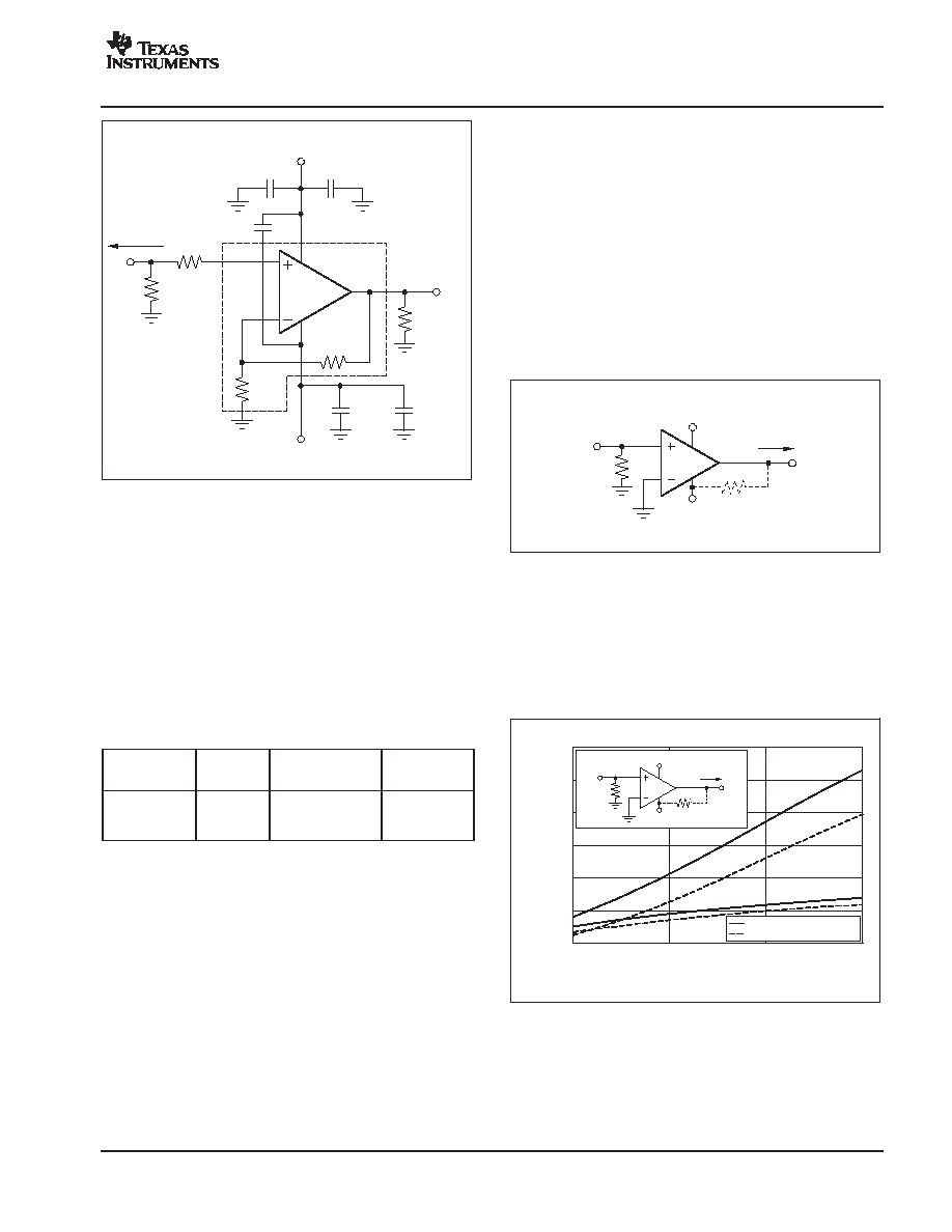
Figure 1 shows the AC-coupled, gain of +2 configuration
used for the +5V Specifications and Typical Characteristic
Curves. The input impedance matching resistor (66.5
)
used for testing is adjusted to give a 50
input match when
the parallel combination of the biasing divider network is
included. Voltage swings reported in the Electrical
Characteristics are taken directly at the input and output
pins. For the circuit of Figure 1, the total effective load on
the output at high frequencies is 150
|| 800
. The 332
and 499
resistors at the noninverting input provide the
common-mode bias voltage. Their parallel combination
equals the DC resistance at the inverting input (R
F
R
G
),
reducing the DC output offset due to input bias current.
OPA832
V
S
= +5V
V
OUT
66.5
V
IN
499
V
CM
= 2V
332
R
L
150
V
CM
= 2V
V
CM
= 2V
6.8
µ
F
+
0.1
µ
F
0.1
µ
F
R
F
400
R
G
400
Figure 1. AC-Coupled, G = +2, +5V Single-Supply
Specification and Test Circuit
Figure 2 shows the AC-coupled, gain of +2 configuration
used for the +3.3V Specifications and Typical
Characteristic Curves. The input impedance matching
resistor (66.5
) used for testing is adjusted to give a 50
input match when the parallel combination of the biasing
divider network is included. Voltage swings reported in the
Electrical Characteristics are taken directly at the input
and output pins. For the circuit of Figure 2, the total
effective load on the output at high frequencies is
150
|| 800
. The 887
and 258
resistors at the
noninverting input provide the common-mode bias
voltage. Their parallel combination equals the DC
resistance at the inverting input (R
F
R
G
), reducing the
DC output offset due to input bias current.
OPA832
V
S
= +3.3V
V
OUT
66.5
V
IN
887
V
CM
= 0.75V
258
R
L
150
V
CM
= 0.75V
V
CM
= 0.75V
6.8
µ
F
+
0.1
µ
F
0.1
µ
F
R
F
400
R
G
400
Figure 2. AC-Coupled, G = +2, +3.3V
Single-Supply Specification and Test Circuit
Figure
3 shows the DC-coupled, gain of +2, dual
power-supply circuit configuration used as the basis of the
±
5V Electrical Characteristics and Typical Characteristics.
For test purposes, the input impedance is set to 50
with
a resistor to ground and the output impedance is set to 50
with a series output resistor. Voltage swings reported in the
specifications are taken directly at the input and output
pins. For the circuit of Figure 3, the total effective load will
be 150
|| 800
. Two optional components are included
in Figure 3. An additional resistor (175
) is included in
series with the noninverting input. Combined with the 25
DC source resistance looking back towards the signal
generator, this gives an input bias current cancelling
resistance that matches the 200
source resistance seen
at the inverting input (see the DC Accuracy and Offset
Control section). In addition to the usual power-supply
decoupling capacitors to ground, a 0.01
µ
F capacitor is
included between the two power-supply pins. In practical
PC board layouts, this optionally-added capacitor will
typically improve the 2nd-harmonic distortion performance
by 3dB to 6dB.
OPA832
SBOS266B - JUNE 2003 - REVISED SEPTEMBER 2004
www.ti.com
15
OPA832
+5V
-
5V
V
OUT
50
V
IN
R
F
400
175
50
Source
150
R
G
400
6.8
µ
F
+
6.8
µ
F
+
0.1
µ
F
0.1
µ
F
0.01
µ
F
Figure 3. DC-Coupled, G = +2, Bipolar Supply
Specification and Test Circuit
DESIGN-IN TOOLS
DEMONSTRATION BOARDS
Several PC boards are available to assist in the initial
evaluation of circuit performance using the OPA832 in its
two package styles. All of these are available, free, as
unpopulated PC boards delivered with descriptive
documentation. The summary information for these
boards is shown in Table 1.
Table 1. Demo Board Availability
PRODUCT
PACKAGE
DEMO BOARD
ORDERING
PRODUCT
PACKAGE
DEMO BOARD
NUMBER
ORDERING
NUMBER
OPA832ID
SO-8
DEM
-
OPA68xU
SBOU009
OPA832IDBV
SOT23-5
DEM
-
OPA6xxN
SBOU010
Go to the TI web site (www.ti.com) to request evaluation
boards through the OPA832 product folder.
MACROMODEL AND APPLICATIONS
SUPPORT
Computer simulation of circuit performance using SPICE
is often a quick way to analyze the performance of the
OPA832 and its circuit designs. This is particularly true for
video and RF amplifier circuits where parasitic
capacitance and inductance can play a major role on
circuit performance. A SPICE model for the OPA832 is
available through the TI web page (www.ti.com). The
applications department is also available for design
assistance. These models predict typical small signal AC,
transient steps, DC performance, and noise under a wide
variety of operating conditions. The models include the
noise terms found in the electrical specifications of the
data sheet. These models do not attempt to distinguish
between the package types in their small-signal AC
performance.
GAIN OF +2V/V VIDEO LINE DRIVER
One of the most suitable applicarions for the OPA832 is a
simple gain of 2 video line driver. Figure 4 shows how
simple this circuit is to implement, shown as a
±
5V
implementation. Single +5V operation is similar with
blocking caps and DC common-mode biasing provided.
OPA832
Video
In
Video
Loads
+5V
-
5V
Optional 1.3k
Pull-Down
Figure 4. Gain of 2 Video Line Driver
One optional element is shown in Figure 4. A 1.3k
pull-down to the negative supply will improve the
differential phase significantly and the differential gain
slightly. Figure 5 shows measured dG/dP with and without
that pull-down resistor from 1 to 4 video loads.
1.2
1.0
0.8
0.6
0.4
0.2
0
Number of 150
Loads
dG
/d
P
1
2
3
4
dG
dP
dG
dP
No Pull-Down
With 1.3k
Pull-Down
OPA832
Video
In
V ide o
L oa ds
+5V
-
5V
O ptio nal 1.3k
Pull-Down
Figure 5. dG/dP vs Video Loads

OPA832
SBOS266B - JUNE 2003 - REVISED SEPTEMBER 2004
www.ti.com
16
SINGLE-SUPPLY ADC INTERFACE
The circuit shown in Figure 6 uses the OPA832 as a
differential driver followed by an RC filter. In this circuit, the
single-ended to differential conversion is realized by a 1:1
transformer driving the noninverting inputs of the two
OPA832s. The common-mode level (CML) of the
ADS5203 is reduced to the appropriate input level of
0.885V by the network divider composed of R
1
and the
CML output impedance, and connected to the transformer
center tap, biasing the OPA832s. This input bias voltage
is then amplified to provide the correct common-mode
voltage to the input of the ADC. Using only 25.1mW power
(3.8mA
◊
2 amplifiers
◊
3.3V), this configuration (amplifier
+ ADC) provides greater than 59dB SNR and 70dB SFDR
to 2MHz, with all the components running on a low +3.3V
supply.
R
F
400
R
G
400
C
15pF
C
1
0.1
µ
F
IN
IN
CML
1/2
ADS5203
10-Bit
40MSPS
OPA832
OPA832
+3.3V
+3.3V
+3.3V
R
F
400
R
G
400
R
I
1.91k
R
S
50
R
S
50
R
T
20
R
T
20
R
M
50
1:1
2.3k
Output
Impedance
V
IN
50
Source
V
CM
= 0.885V
Figure 6. Low-Power, Single-Supply ADC Driver

OPA832
SBOS266B - JUNE 2003 - REVISED SEPTEMBER 2004
www.ti.com
17
This circuit removes the peaking by bootstrapping out any
parasitic effects on R
G
. The input impedance is still set by
R
M
as the apparent impedance looking into R
G
is very
high. R
M
may be increased to show a higher input
impedance, but larger values will start to impact DC output
offset voltage. This circuit creates an additional input offset
voltage as the difference in the two input bias current times
the impedance to ground at V
IN
. Figure 8 shows a
comparison of small-signal frequency response for the
unity-gain buffer of Figure 2 (with V
CM
removed from R
G
)
compared to the improved approach shown in Figure 7.
OPA832
V
OUT
V
IN
R
G
400
R
O
75
R
F
400
R
M
50
+5V
Figure 7. Improved Unity-Gain Buffer
UNITY-GAIN BUFFER
This buffer can simply be realized by not connecting R
G
to
ground. This type of realization shows a peaking in the
frequency response. A similar circuit that holds a flat
frequency response giving improved pulse fidelity is
shown in Figure 7.
6
3
0
-
3
-
6
-
9
-
12
Frequency (MHz)
Ga
i
n
(
d
B
)
1
10
100
400
G = +1 Buffer
R
G
Floating
G = +1 Buffer
Figure 5
Figure 8. Buffer Frequency Response
Comparison
OPERATING SUGGESTIONS
GAIN SETTING
Setting the gain for the OPA832 is very easy. For a gain of
+2, ground the -IN pin and drive the +IN pin with the signal.
For a gain of +1, either leave the -IN pin open and drive the
+IN pin or drive both the +IN and -IN pins as shown in
Figure 7. For a gain of -1, ground the +IN pin and drive the
-IN pin with the input signal. An external resistor may be
used in series with the -IN pin to reduce the gain. However,
since the internal resistors (R
F
and R
G
) have a tolerance
and temperature drift different than the external resistor,
the absolute gain accuracy and gain drift over temperature
will be relatively poor compared to the previously
described standard gain connections using no external
resistor.
OUTPUT CURRENT AND VOLTAGES
The OPA832 provides outstanding output voltage
capability. Under no-load conditions at +25
∞
C, the output
voltage typically swings closer than 90mV to either supply
rail.
The minimum specified output voltage and current
specifications over temperature are set by worst-case
simulations at the cold temperature extreme. Only at cold
startup will the output current and voltage decrease to the
numbers shown in the min/max tables. As the output
transistors deliver power, their junction temperatures will
increase, decreasing their V
BE
s (increasing the available
output voltage swing) and increasing their current gains
(increasing the available output current). In steady-state
operation, the available output voltage and current will
always be greater than that shown in the over-temperature
specifications, since the output stage junction
temperatures will be higher than the minimum specified
operating ambient.
To maintain maximum output stage linearity, no output
short-circuit protection is provided. This will not normally
be a problem, since most applications include a series
matching resistor at the output that will limit the internal
power dissipation if the output side of this resistor is
shorted to ground. However, shorting the output pin
directly to the adjacent positive power-supply pin (8-pin
packages) will possibly destroy the amplifier. If additional
short-circuit protection is required, consider a small series
resistor in the power-supply leads. This will reduce the
available output voltage swing under heavy output loads.
DRIVING CAPACITIVE LOADS
One of the most demanding and yet very common load
conditions for an op amp is capacitive loading. Often, the
capacitive load is the input of an ADC--including
additional external capacitance which may be recom-
mended to improve ADC linearity. A high-speed, high
open-loop gain amplifier like the OPA832 can be very
susceptible to decreased stability and closed-loop
response peaking when a capacitive load is placed directly
on the output pin. When the primary considerations are
frequency response flatness, pulse response fidelity,

OPA832
SBOS266B - JUNE 2003 - REVISED SEPTEMBER 2004
www.ti.com
18
and/or distortion, the simplest and most effective solution
is to isolate the capacitive load from the feedback loop by
inserting a series isolation resistor between the amplifier
output and the capacitive load.
The Typical Characteristic curves show the recommended
R
S
versus capacitive load and the resulting frequency
response at the load. Parasitic capacitive loads greater
than 2pF can begin to degrade the performance of the
OPA832. Long PC board traces, unmatched cables, and
connections to multiple devices can easily exceed this
value. Always consider this effect carefully, and add the
recommended series resistor as close as possible to the
output pin (see the Board Layout Guidelines section).
The criterion for setting this R
S
resistor is a 1dB peaked
frequency response at the load. Increasing the noise gain
will also reduce the peaking (see Figure 7).
DISTORTION PERFORMANCE
The OPA832 provides good distortion performance into a
150
load. Relative to alternative solutions, it provides
exceptional performance into lighter loads and/or
operating on a single +3.3V supply. Generally, until the
fundamental signal reaches very high frequency or power
levels, the 2nd-harmonic will dominate the distortion with
a negligible 3rd-harmonic component. Focusing then on
the 2nd-harmonic, increasing the load impedance
improves distortion directly. Remember that the total load
includes the feedback network; in the noninverting
configuration (see Figure 3) this is sum of R
F
+ R
G
, while
in the inverting configuration, only R
F
needs to be included
in parallel with the actual load.
Figure 9 shows the 2nd- and 3rd-harmonic distortion
versus supply voltage. In order to maintain the input signal
within acceptable operating range, the input
common-mode voltage is adjusted for each supply
voltage. For example, the common-mode voltage is +2V
for a single +5V supply, and the distortion is -66.5dBc for
the 2nd-harmonic and -74.6dBc for the 3rd-harmonic.
-
66
-
67
-
68
-
69
-
70
-
71
-
72
-
73
-
74
-
75
-
76
Supply Voltage (V)
H
a
r
m
oni
c
D
i
s
tor
t
i
o
n
(
dB
c
)
5.5
5.0
4.5
4.0
3.5
3.0
2.5
2.0
1.5
1.0
0.5
C
o
m
m
on-
Mode
V
o
l
t
a
g
e
(
V
)
5
6
7
8
9
10
11
G = +2V/V
R
L
= 500
V
O
= 2V
PP
f = 5MHz
Common-Mode Voltage
Right Scale
2nd-Harmonic
Left Scale
3rd-Harmonic
Left Scale
Figure 9. 5MHz Harmonic Distortion vs Supply
Voltage
NOISE PERFORMANCE
Unity-gain stable, rail-to-rail (RR) output, voltage-feed-
back op amps usually show a higher input noise voltage.
The 9.2nV/
Hz input voltage noise for the OPA832
however, is much lower than comparable amplifiers. The
input-referred voltage noise and the two input-referred
current noise terms (2.8pA/
Hz) combine to give low
output noise under a wide variety of operating conditions.
Figure 10 shows the op amp noise analysis model with all
the noise terms included. In this model, all noise terms are
taken to be noise voltage or current density terms in either
nV/
Hz or pA/
Hz.
4kT
R
G
R
G
R
F
R
S
OPA832
I
BI
E
O
I
BN
4kT = 1.6E
-
20J
at 290
_
K
E
RS
E
NI
4kTR
S
4kTR
F
Figure 10. Noise Analysis Model
The total output spot noise voltage can be computed as the
square root of the sum of all squared output noise voltage
contributors. Equation 1 shows the general form for the
output noise voltage using the terms shown in Figure 10:
E
O
+
ENI
2
)
IBNRS
2
)
4kTR
S
NG2
)
IBIRF
2
)
4kTRFNG
Dividing this expression by the noise gain
(NG = (1 + R
F
/R
G
)) will give the equivalent input-referred
spot noise voltage at the noninverting input, as shown in
Equation 2:
E
N
+
E
NI
2
)
I
BN
R
S
2
)
4kTR
S
)
I
BI
R
F
NG
2
)
4kTR
F
NG
Evaluating these two equations for the circuit and
component values shown in Figure 1 will give a total output
spot noise voltage of 19.3nV/
Hz and a total equivalent
input spot noise voltage of 9.65nV/
Hz. This is including
the noise added by the resistors. This total input-referred
spot noise voltage is not much higher than the 9.2nV/
Hz
specification for the op amp voltage noise alone.
(1)
(2)

OPA832
SBOS266B - JUNE 2003 - REVISED SEPTEMBER 2004
www.ti.com
19
DC ACCURACY AND OFFSET CONTROL
The balanced input stage of a wideband voltage-feedback
op amp allows good output DC accuracy in a wide variety
of applications. The power-supply current trim for the
OPA832 gives even tighter control than comparable
products. Although the high-speed input stage does
require relatively high input bias current (typically 5
µ
A out
of each input terminal), the close matching between them
may be used to reduce the output DC error caused by this
current. This is done by matching the DC source
resistances appearing at the two inputs. Evaluating the
configuration of Figure 3 (which has matched DC input
resistances), using worst-case +25
∞
C input offset voltage
and current specifications, gives a worst-case output
offset voltage equal to:
(NG = noninverting signal gain at DC)
±
(NG
◊
V
OS(MAX)
)
±
(R
F
◊
I
OS(MAX)
)
=
±
(2
◊
10mV)
±
(400
◊
1.5
µ
A)
=
±
10.6mV
A fine-scale output offset null, or DC operating point
adjustment, is often required. Numerous techniques are
available for introducing DC offset control into an op amp
circuit. Most of these techniques are based on adding a DC
current through the feedback resistor. In selecting an offset
trim method, one key consideration is the impact on the
desired signal path frequency response. If the signal path
is intended to be noninverting, the offset control is best
applied as an inverting summing signal to avoid interaction
with the signal source. If the signal path is intended to be
inverting, applying the offset control to the noninverting
input may be considered. Bring the DC offsetting current
into the inverting input node through resistor values that
are much larger than the signal path resistors. This will
insure that the adjustment circuit has minimal effect on the
loop gain and hence the frequency response.
THERMAL ANALYSIS
Maximum desired junction temperature will set the
maximum allowed internal power dissipation, as
described below. In no case should the maximum junction
temperature be allowed to exceed 150
∞
C.
Operating junction temperature (T
J
) is given by
T
A
+ P
D
◊ q
JA
. The total internal power dissipation (P
D
)
is the sum of quiescent power (P
DQ
) and additional
power dissipated in the output stage (P
DL
) to deliver load
power. Quiescent power is simply the specified no-load
supply current times the total supply voltage across the
part. P
DL
will depend on the required output signal and
load; though, for resistive loads connected to
mid-supply (V
S
/2), P
DL
is at a maximum when the output
is fixed at a voltage equal to V
S
/4 or 3V
S
/4. Under this
condition, P
DL
= V
S
2
/(16
◊
R
L
), where R
L
includes
feedback network loading.
Note that it is the power in the output stage, and not into the
load, that determines internal power dissipation.
As a worst-case example, compute the maximum T
J
using
an OPA832 (SOT23-5 package) in the circuit of Figure 3
operating at the maximum specified ambient temperature
of +85
∞
C and driving a 150
load at mid-supply.
P
D
= 10V
◊
3.9mA + 5
2
/(16
◊
(150
|| 400
)) = 53.3mW
Maximum T
J
= +85
∞
C + (0.053W
◊
150
∞
C/W) = 93
∞
C.
Although this is still well below the specified maximum
junction temperature, system reliability considerations
may require lower ensured junction temperatures. The
highest possible internal dissipation will occur if the load
requires current to be forced into the output at high output
voltages or sourced from the output at low output voltages.
This puts a high current through a large internal voltage
drop in the output transistors.
BOARD LAYOUT GUIDELINES
Achieving optimum performance with a high-frequency
amplifier like the OPA832 requires careful attention to
board layout parasitics and external component types.
Recommendations that will optimize performance include:
a) Minimize parasitic capacitance to any AC ground for
all of the signal I/O pins. Parasitic capacitance on the
output and inverting input pins can cause instability: on the
noninverting input, it can react with the source impedance
to cause unintentional bandlimiting. To reduce unwanted
capacitance, a window around the signal I/O pins should
be opened in all of the ground and power planes around
those pins. Otherwise, ground and power planes should
be unbroken elsewhere on the board.
b) Minimize the distance ( < 0.25") from the power-supply
pins to high-frequency 0.1
µ
F decoupling capacitors. At the
device pins, the ground and power-plane layout should not
be in close proximity to the signal I/O pins. Avoid narrow
power and ground traces to minimize inductance between
the pins and the decoupling capacitors. Each power-
supply connection should always be decoupled with one
of these capacitors. An optional supply decoupling
capacitor (0.1
µ
F) across the two power supplies (for
bipolar operation) will improve 2nd-harmonic distortion
performance. Larger (2.2
µ
F to 6.8
µ
F) decoupling
capacitors, effective at lower frequency, should also be
used on the main supply pins. These may be placed
somewhat farther from the device and may be shared
among several devices in the same area of the PC board.
c) Careful selection and placement of external
components will preserve the high-frequency perfor-
mance. Resistors should be a very low reactance type.
Surface-mount resistors work best and allow a tighter
overall layout. Metal film or carbon composition
axially-leaded resistors can also provide good high-
frequency performance. Again, keep their leads and PC
OPA832
SBOS266B - JUNE 2003 - REVISED SEPTEMBER 2004
www.ti.com
20
board traces as short as possible. Never use wire-wound
type resistors in a high-frequency application. Since the
output pin is the most sensitive to parasitic capacitance,
always position the series output resistor, if any, as close
as possible to the output pin. Other network components,
such as noninverting input termination resistors, should
also be placed close to the package.
d) Connections to other wideband devices on the board
may be made with short direct traces or through onboard
transmission lines. For short connections, consider the
trace and the input to the next device as a lumped
capacitive load. Relatively wide traces (50mils to 100mils)
should be used, preferably with ground and power planes
opened up around them. Estimate the total capacitive load
and set R
S
from the typical characteristic curve
Recommended R
S
vs Capacitive Load. Low parasitic
capacitive loads (< 5pF) may not need an R
S
since the
OPA832 is nominally compensated to operate with a 2pF
parasitic load. Higher parasitic capacitive loads without an
R
S
are allowed as the signal gain increases (increasing the
unloaded phase margin). If a long trace is required, and the
6dB signal loss intrinsic to a doubly-terminated
transmission line is acceptable, implement a matched
impedance transmission line using microstrip or stripline
techniques (consult an ECL design handbook for
microstrip and stripline layout techniques). A 50
environment is normally not necessary onboard, and in
fact, a higher impedance environment will improve
distortion as shown in the distortion versus load plots. With
a characteristic board trace impedance defined (based on
board material and trace dimensions), a matching series
resistor into the trace from the output of the OPA832 is
used as well as a terminating shunt resistor at the input of
the destination device. Remember also that the
terminating impedance will be the parallel combination of
the shunt resistor and the input impedance of the
destination device; this total effective impedance should
be set to match the trace impedance. If the 6dB attenuation
of a doubly-terminated transmission line is unacceptable,
a long trace can be series-terminated at the source end
only. Treat the trace as a capacitive load in this case and
set the series resistor value as shown in the typical
characteristic curve Recommended R
S
vs Capacitive
Load. This will not preserve signal integrity as well as a
doubly-terminated line. If the input impedance of the
destination device is low, there will be some signal
attenuation due to the voltage divider formed by the series
output into the terminating impedance.
e) Socketing a high-speed part is not recommended.
The additional lead length and pin-to-pin capacitance
introduced by the socket can create an extremely
troublesome parasitic network which can make it almost
impossible to achieve a smooth, stable frequency
response. Best results are obtained by soldering the
OPA832 onto the board.
INPUT AND ESD PROTECTION
The OPA832 is built using a very high-speed complemen-
tary bipolar process. The internal junction breakdown
voltages are relatively low for these very small geometry
devices. These breakdowns are reflected in the Absolute
Maximum Ratings table. All device pins are protected
with internal ESD protection diodes to the power supplies,
as shown in Figure 11.
External
Pin
+V
CC
- V
CC
Internal
Circuitry
Figure 11. Internal ESD Protection
These diodes provide moderate protection to input
overdrive voltages above the supplies as well. The
protection diodes can typically support 30mA continuous
current. Where higher currents are possible (that is, in
systems with
±
15V supply parts driving into the OPA832),
current-limiting series resistors should be added into the
two inputs. Keep these resistor values as low as possible,
since high values degrade both noise performance and
frequency response.

PACKAGING INFORMATION
ORDERABLE DEVICE
STATUS(1)
PACKAGE TYPE
PACKAGE DRAWING
PINS
PACKAGE QTY
OPA832ID
ACTIVE
SO-8
D
8
100
OPA832IDR
ACTIVE
SO-8
D
8
2500
OPA832DBVT
ACTIVE
SOT23
DBV
5
250
OPA832DBVR
ACTIVE
SOT23
DBV
5
3000
(1) The marketing status values are defined as follows:
ACTIVE: Product device recommended for new designs.
LIFEBUY: TI has announced that the device will be discontinued, and a lifetime-buy period is in effect.
NRND: Not recommended for new designs. Device is in production to support existing customers, but TI does not recommend using this part in
a new design.
PREVIEW: Device has been announced but is not in production. Samples may or may not be available.
OBSOLETE: TI has discontinued the production of the device.
PACKAGE OPTION ADDENDUM
www.ti.com
15-Sep-2004
(2) Eco-Status information
Additional details including specific material content can be accessed at www.ti.com/leadfree
GREEN: Ti defines Green to mean Lead (Pb)-Free and in addition, uses less package materials that do not contain halogens, including
bromine (Br), or antimony (Sb) above 0.1% of total product weight.
N/A: Not yet available Lead (Pb)-Free; for estimated conversion dates, go to www.ti.com/leadfree.
Pb-FREE: Ti defines Lead (Pb)-Free to mean RoHS compatible, including a lead concentration that does not exceed 0.1% of total product
weight, and, if designed to be soldered, suitable for use in specified lead-free soldering processes.
N/A
Pb-Free, Green
ECO-STATUS(2)
Pb-Free, Green
N/A


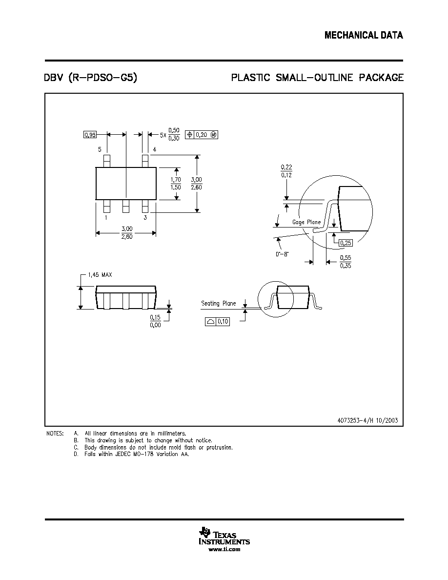


IMPORTANT NOTICE
Texas Instruments Incorporated and its subsidiaries (TI) reserve the right to make corrections, modifications,
enhancements, improvements, and other changes to its products and services at any time and to discontinue
any product or service without notice. Customers should obtain the latest relevant information before placing
orders and should verify that such information is current and complete. All products are sold subject to TI's terms
and conditions of sale supplied at the time of order acknowledgment.
TI warrants performance of its hardware products to the specifications applicable at the time of sale in
accordance with TI's standard warranty. Testing and other quality control techniques are used to the extent TI
deems necessary to support this warranty. Except where mandated by government requirements, testing of all
parameters of each product is not necessarily performed.
TI assumes no liability for applications assistance or customer product design. Customers are responsible for
their products and applications using TI components. To minimize the risks associated with customer products
and applications, customers should provide adequate design and operating safeguards.
TI does not warrant or represent that any license, either express or implied, is granted under any TI patent right,
copyright, mask work right, or other TI intellectual property right relating to any combination, machine, or process
in which TI products or services are used. Information published by TI regarding third-party products or services
does not constitute a license from TI to use such products or services or a warranty or endorsement thereof.
Use of such information may require a license from a third party under the patents or other intellectual property
of the third party, or a license from TI under the patents or other intellectual property of TI.
Reproduction of information in TI data books or data sheets is permissible only if reproduction is without
alteration and is accompanied by all associated warranties, conditions, limitations, and notices. Reproduction
of this information with alteration is an unfair and deceptive business practice. TI is not responsible or liable for
such altered documentation.
Resale of TI products or services with statements different from or beyond the parameters stated by TI for that
product or service voids all express and any implied warranties for the associated TI product or service and
is an unfair and deceptive business practice. TI is not responsible or liable for any such statements.
Following are URLs where you can obtain information on other Texas Instruments products and application
solutions:
Products
Applications
Amplifiers
amplifier.ti.com
Audio
www.ti.com/audio
Data Converters
dataconverter.ti.com
Automotive
www.ti.com/automotive
DSP
dsp.ti.com
Broadband
www.ti.com/broadband
Interface
interface.ti.com
Digital Control
www.ti.com/digitalcontrol
Logic
logic.ti.com
Military
www.ti.com/military
Power Mgmt
power.ti.com
Optical Networking
www.ti.com/opticalnetwork
Microcontrollers
microcontroller.ti.com
Security
www.ti.com/security
Telephony
www.ti.com/telephony
Video & Imaging
www.ti.com/video
Wireless
www.ti.com/wireless
Mailing Address:
Texas Instruments
Post Office Box 655303 Dallas, Texas 75265
Copyright
2004, Texas Instruments Incorporated