 | ÐлекÑÑоннÑй компоненÑ: OPT211 | СкаÑаÑÑ:  PDF PDF  ZIP ZIP |
Äîêóìåíòàöèÿ è îïèñàíèÿ www.docs.chipfind.ru
©
1994 Burr-Brown Corporation
PDS-1258B
Printed in U.S.A. January, 1995
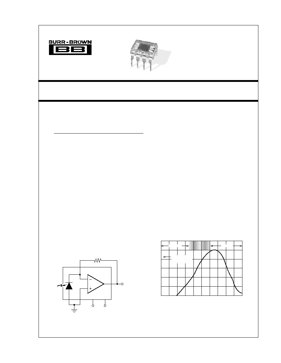
OPT211
MONOLITHIC PHOTODIODE AND AMPLIFIER
DESCRIPTION
The OPT211 is a monolithic photodiode with on-chip
FET-input transpedance amplifier, that provides wide
bandwidth at very high gains. Uncommitted input and
feedback nodes allow a variety of feedback options for
maximum versatility. Trade-offs in responsivity (gain),
bandwidth and SNR can easily be made.
The monolithic combination of photodiode and
transimpedance amplifier on a single chip eliminates
the problems commonly encountered in discrete de-
signs such as leakage current errors, noise pickup and
gain peaking due to stray capacitance. The 0.09
x
0.09
inch photodiode is operated at zero bias for excellent
linearity and low dark current. Direct access to the
detector's anode allows photodiode bootstrapping,
which increases speed performance.
The OPT211 operates over a wide supply range (
±
2.25V
to
±
18V) and supply current is only 400
µ
A. It is
packaged in a transparent plastic 8-pin DIP specified
for the 0
°
C to 70
°
C temperature range.
OPT211
7
8
3
1
5
V
OUT
2
V
V+
R
F
FEATURES
q
WIDE BANDWIDTH, HIGH RESPONSIVITY:
R
F
BANDWIDTH
1M
50kHz
*150kHz
100M
5kHz
*13kHz
*with bootstrap buffer
q
PHOTODIODE SIZE: 0.090 x 0.090 inch
(2.29 x 2.29mm)
q
HIGH RESPONSIVITY: 0.45A/W
(650nm)
q
LOW DARK ERRORS: 2mV max
q
EXCELLENT SPECTRAL RESPONSE
q
LOW QUIESCENT CURRENT: 400
µ
A
q
TRANSPARENT 8-PIN DIP
APPLICATIONS
q
MEDICAL INSTRUMENTATION
q
LABORATORY INSTRUMENTATION
q
POSITION AND PROXIMITY SENSORS
q
PHOTOGRAPHIC ANALYZERS
q
BARCODE SCANNERS
q
SMOKE DETECTORS
SPECTRAL RESPONSIVITY
Photodiode Responsivity (A/W)
Wavelength (nm)
100
200
300
400 500
600
700 800
900 1000 1100
0.5
0.4
0.3
0.2
0.1
0
Infrared
Blue
Green
Yellow
Red
Ultraviolet
Using External
1M
Resistor
®
International Airport Industrial Park · Mailing Address: PO Box 11400, Tucson, AZ 85734 · Street Address: 6730 S. Tucson Blvd., Tucson, AZ 85706 · Tel: (520) 746-1111 · Twx: 910-952-1111
Internet: http://www.burr-brown.com/ · FAXLine: (800) 548-6133 (US/Canada Only) · Cable: BBRCORP · Telex: 066-6491 · FAX: (520) 889-1510 · Immediate Product Info: (800) 548-6132

®
OPT211
2
SPECIFICATIONS
At T
A
= +25
°
C, V
S
=
±
15V,
= 650nm, external 1M
feedback resistor, circuit shown in Figure 1, unless otherwise noted.
The information provided herein is believed to be reliable; however, BURR-BROWN assumes no responsibility for inaccuracies or omissions. BURR-BROWN assumes
no responsibility for the use of this information, and all use of such information shall be entirely at the user's own risk. Prices and specifications are subject to change
without notice. No patent rights or licenses to any of the circuits described herein are implied or granted to any third party. BURR-BROWN does not authorize or warrant
any BURR-BROWN product for use in life support devices and/or systems.
Photodiode of OPT211
PARAMETER
CONDITIONS
MIN
TYP
MAX
UNITS
Photodiode Area
(0.090 x 0.090 inches)
0.008
in
2
(2.29 x 2.29mm)
5.2
mm
2
Current Responsivity
= 650nm
0.45
A/W
865
µ
A/W/cm
2
Dark Current
V
D
= 0V
500
fA
vs Temperature
doubles every 10
°
C
Capacitance
V
D
= 0V
600
pF
PHOTODIODE SPECIFICATIONS
At T
A
= +25
°
C,
= 650nm, unless otherwise noted.
OPT211P
PARAMETER
CONDITIONS
MIN
TYP
MAX
UNITS
RESPONSIVITY
Photodiode Current
650nm
0.45
A/W
Unit-to-Unit Variation
650nm
±
5
%
Voltage Output
= 650nm, R
F
= 1M
0.45
V/
µ
W
Nonlinearity
0.01
% of FS
Photodiode Area
(0.090 x 0.090 inches)
0.008
in
2
(2.29 x 2.29mm)
5.2
mm
2
DARK ERRORS, RTO
(1)
Offset Voltage, Output
±
0.5
±
2
mV
vs Temperature
±
10
µ
V/
°
C
vs Power Supply
V
S
=
±
2.25V to
±
18V
10
100
µ
V/V
Voltage Noise, Dark
Dark, f
B
= 0.1Hz to 100kHz
1
mVrms
FREQUENCY RESPONSE
Bandwidth
Anode Grounded
(2)
50
kHz
Anode Bootstrapped
(3)
150
kHz
Rise Time, 10% to 90%, R
F
= 1M
Anode Grounded
(2)
5
µ
s
Anode Bootstrapped
(3)
2
µ
s
Settling Time, FS to Dark
Anode Grounded
(2)
1%
10
µ
s
0.1%
25
µ
s
0.01%
30
µ
s
100% Overload Recovery Time
FS to Dark (to 1%)
44
µ
s
V
S
=
±
5V
100
µ
s
V
S
=
±
2.25V
240
µ
s
OUTPUT
Voltage Output
R
L
= 10k
(V+) 1.25
(V+) 1
V
R
L
= 5k
(V+) 2
(V+) 1.5
V
Capacitive Load, Stable Operation
(4)
250
pF
Short-Circuit Current
±
18
mA
POWER SUPPLY
Operating Voltage Range
±
2.25
±
15
±
18
V
Quiescent Current
V
OUT
= 0V
±
400
±
500
µ
A
TEMPERATURE RANGE
Specification
0
+70
°
C
Operating
0
+70
°
C
Storage
25
+85
°
C
Thermal Resistance,
JA
100
°
C/W
NOTES: (1) Referred to Output. Includes all error sources. (2) See Figure 1. (3) See Figure 3. (4) See Figure 2.

®
OPT211
3
OP AMP SPECIFICATIONS
T
A
= +25
°
C, V
S
=
±
15V, R
L
= 10k
, unless otherwise noted.
OPT211 Op Amp
(1)
PARAMETER
CONDITIONS
MIN
TYP
MAX
UNITS
INPUT
Offset Voltage
±
0.5
mV
vs Temperature
±
5
µ
V/
°
C
vs Power Supply
V
S
=
±
2.25V to
±
18V
10
µ
V/V
Input Bias Current
±
1
pA
vs Temperature
doubles every 10
°
C
Input Impedance
Differential
10
12
|| 3
|| pF
Common-Mode
10
12
|| 3
|| pF
Common-Mode Input Voltage Range
Linear Operation
±
14.4
V
Common-Mode Rejection
106
dB
NOISE
Voltage Noise Density
f = 10Hz
30
nV/
Hz
f = 100Hz
25
nV/
Hz
f = 1kHz
15
nV/
Hz
Current Noise Density
f = 1kHz
0.8
fA/
Hz
OPEN-LOOP GAIN
Open-Loop Voltage Gain
120
dB
FREQUENCY RESPONSE
Gain-Bandwidth Product
(2)
16
MHz
Slew Rate
6
V/
µ
s
Settling Time 0.1%
4
µ
s
0.01%
5
µ
s
OUTPUT
Voltage Output
R
L
= 10k
(V+) 1.25
(V+) 1
V
R
L
= 5k
(V+) 2
(V+) 1.5
V
Short-Circuit Current
±
18
mA
POWER SUPPLY
Operating Voltage Range
±
2.25
±
15
±
18
V
Quiescent Current
I
O
= 0mA
±
400
±
500
µ
A
NOTES: (1) Op amp specifications provided for information and comparison only. (2) Stable in gains
20V/V.
®
OPT211
4
ELECTROSTATIC
DISCHARGE SENSITIVITY
This integrated circuit can be damaged by ESD. Burr-Brown
recommends that all integrated circuits be handled with ap-
propriate precautions. Failure to observe proper handling and
installation procedures can cause damage.
ESD damage can range from subtle performance degradation
to complete device failure. Precision integrated circuits may
be more susceptible to damage because very small parametric
changes could cause the device not to meet its published
specifications.
PACKAGE DRAWING
PRODUCT
PACKAGE
NUMBER
(1)
OPT211P
8-Pin DIP
006-1
NOTE: (1) For detailed drawing and dimension table, please see end of data
sheet, or Appendix C of Burr-Brown IC Data Book.
PIN CONFIGURATIONS
MOISTURE SENSITIVITY
AND SOLDERING
Clear plastic does not contain the structural-enhancing fillers
used in black plastic molding compound. As a result, clear
plastic is more sensitive to environmental stress than black
plastic. This can cause difficulties if devices have been stored
in high humidity prior to soldering. The rapid heating during
soldering can stress wire bonds and cause failures. Prior to
soldering, it is recommended that plastic devices be baked-out
at +85
°
C for 24 hours.
The fire-retardant fillers used in black plastic are not compat-
ible with clear molding compound. The OPT211 plastic
packages cannot meet flammability test, UL-94.
Top View
DIP
ABSOLUTE MAXIMUM RATINGS
Supply Voltage ...................................................................................
±
18V
Input Voltage Range ............................................................................
±
V
S
Output Short-Circuit (to ground) ............................................... Continuous
Operating Temperature ..................................................... 25
°
C to +85
°
C
Storage Temperature ........................................................ 25
°
C to +85
°
C
Junction Temperature ...................................................................... +85
°
C
Lead Temperature (soldering, 10s) ................................................ +300
°
C
(Vapor-Phase Soldering Not Recommended)
PACKAGE INFORMATION
V+
In
V
NC
Common
PD Anode
NC
V
OUT
1
2
3
4
8
7
6
5
(1)
NOTE: (1) Photodiode location.
®
OPT211
5
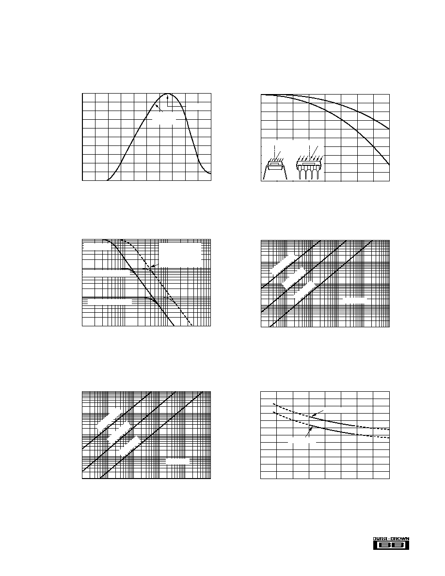
QUIESCENT CURRENT vs TEMPERATURE
Quiescent Current (mA)
Temperature (°C)
75
0.6
0.5
0.4
0.3
0.2
0.1
0
50
25
0
25
50
75
100
125
V
S
= ±15V
V
S
= ±2.25V
VOLTAGE RESPONSIVITY vs IRRADIANCE
Irradiance (W/m
2
)
Output Voltage (V)
10
-4
10
-3
10
-1
10
10
1
10
-2
10
1
0.1
0.01
0.001
R
F
= 10M
R
F
= 1M
R
F
= 100M
= 650nm
VOLTAGE RESPONSIVITY vs RADIANT POWER
Radiant Power (µW)
Output Voltage (V)
10
-3
10
-2
10
10
1
10
2
10
-1
10
1
0.1
0.01
0.001
R
F
= 10M
R
F
= 1M
R
F
= 100M
= 650nm
TRANSIMPEDANCE vs FREQUENCY
Transimpedance (V/A)
Frequency (Hz)
1k
10k
100k
1M
100M
10M
1M
100k
Dotted Line:
Bandwidth with
Bootstrap Buffer--
See Text.
R
F
= 100M
R
F
= 1M
,
C
F
= 3pF
R
F
= 10M
,
C
F
= 1pF
RESPONSE vs INCIDENT ANGLE
Relative Response
Incident Angle (°)
0
1.0
0.8
0.6
0.4
0.2
0
±20
±40
±60
±80
Y
X
1.0
0.8
0.6
0.4
0.2
0
Y
X
Plastic
DIP Package
NORMALIZED SPECTRAL RESPONSIVITY
Normalized Current or Voltage Output
Wavelength (nm)
100
200
300
400 500
600
700 800
900 1000 1100
1.0
0.8
0.6
0.4
0.2
0
650nm
(0.45A/W)
(0.48A/W)
TYPICAL PERFORMANCE CURVES
At T
A
= +25
°
C, V
S
=
±
15V,
= 650nm, external 1M
feedback resistor, circuit shown in Figure 1, unless otherwise noted.
®
OPT211
6
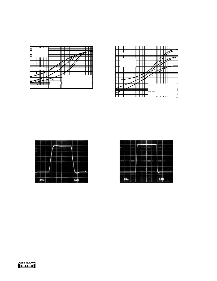
NOISE EFFECTIVE POWER
vs MEASUREMENT BANDWIDTH
Frequency (Hz)
Noise Effective Power (W)
1
10
1k
10k
100k
100
10
8
10
9
10
10
10
11
10
12
10
13
10
14
1M
1M
10M
100M
= 650nm
OPT211 Anode
Grounded
OPT211 with Anode
Bootstrap Drive
Total Noise
0.1 Hz to
Indicated BW
OUTPUT NOISE VOLTAGE
vs MEASUREMENT BANDWIDTH
Frequency (Hz)
Noise Voltage (Vrms)
1
10
1k
10k
100k
100
10
2
10
3
10
4
10
5
10
6
10
7
1M
R
F
= 1M
R
F
= 10M
R
F
= 100M
OPT211 Anode
Grounded
OPT211 with Anode
Bootstrap Drive
Total Noise
0.1 Hz to
Indicated BW
TYPICAL PERFORMANCE CURVES
(CONT)
At T
A
= +25
°
C, V
S
=
±
15V,
= 650nm, external 1M
feedback resistor, circuit shown in Figure 1, unless otherwise noted.
STEP RESPONSE
R
F
= 1M
, Bootstrap Buffer
STEP RESPONSE
R
F
= 1M
, Anode Grounded
®
OPT211
7
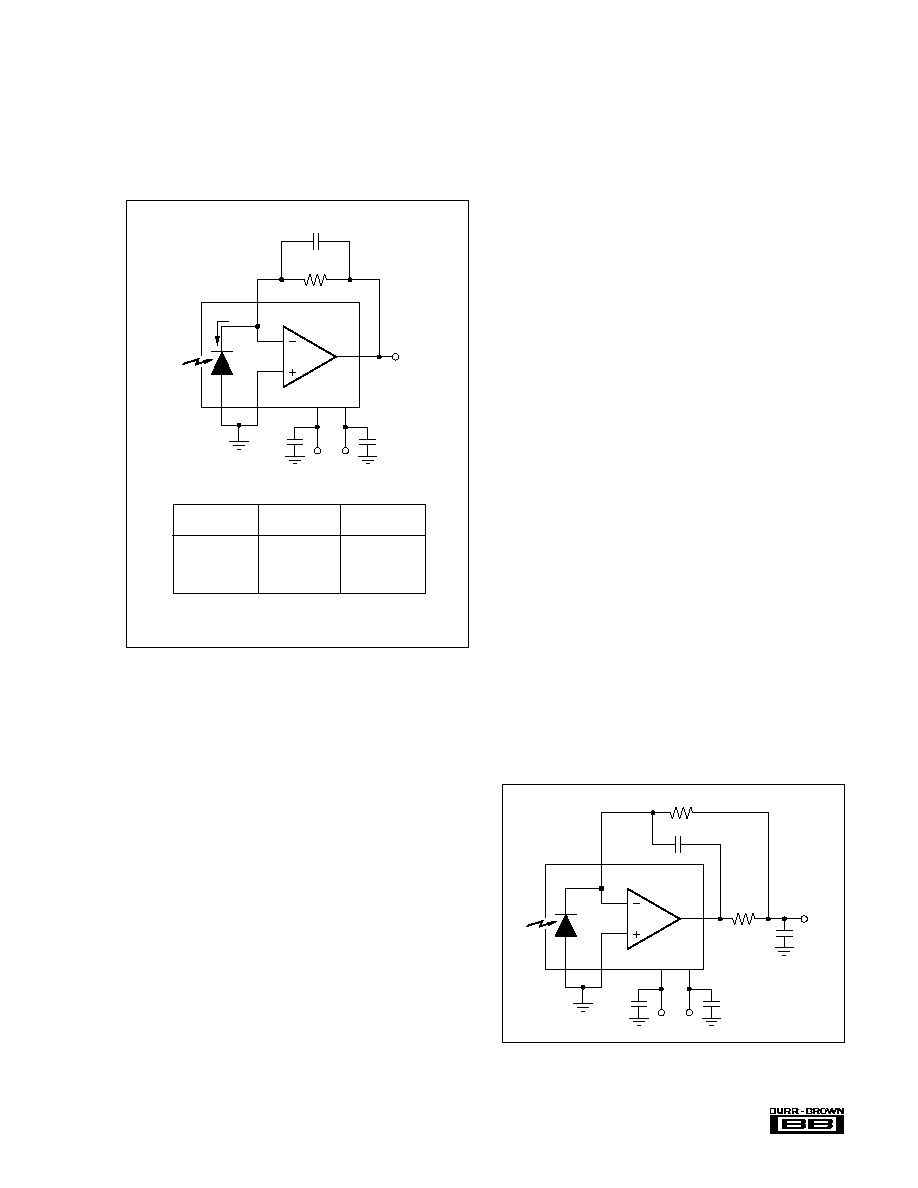
APPLICATIONS INFORMATION
Figure 1 shows the basic connections required to operate the
OPT211. Applications with high impedance power supplies
may require decoupling capacitors located close to the
device pins as shown in Figure 1.
R
F
C
F
Bandwidth
(
)
(pF)
(kHz)
330k
5.6
86
1M
3
50
10M
1
(1)
16
100M
0.3
(1)
5
NOTE: (1) Feedback resistor has approximately 1pF stray
capacitance. C
F
<1pF requires series-connected feedback
resistors. See text.
stray capacitance to a few tenths of a picofarad. With
experimentation, circuit board traces can be used to produce
the necessary stray capacitance for proper compensation and
widest possible bandwidth.
The circuit in Figure 1 can drive capacitive loads up to
250pF. To drive load capacitance up to 1nF, connect R
1
and
the feedback components as shown in Figure 2.
DARK ERRORS
Dark error specifications include all error sources and are
tested with the circuit shown in Figure 1 using R
F
=1M
.
The dominate dark error source is the input offset voltage of
the internal op amp. The combination of photodiode dark
current and op amp input bias current is approximately
1.5pA at 25
°
C. Even with very large feedback resistors, this
contributes virtually no offset error. Dark current and input
bias current increase with temperature, doubling (approxi-
mately) for each 10
°
C increase. At 70
°
C, dark current is
approximately 35pA. This would produce 3.5mV offset with
a 100M
feedback resistor.
Circuit board leakage currents can increase dark error. Use
clean assembly procedures to avoid contamination, particu-
larly around the sensitive inverting input node (pin 2). Errors
due to leakage current from the V+ supply (pin 1) can be
eliminated by encircling the trace connecting to pin 2 with
a guard trace connected to ground.
IMPROVING BANDWIDTH
Bandwidth of the OPT211 can be increased with the feed-
back buffer circuits shown in Figure 3. Driving the anode of
the photodiode (pin 7) in this manner reduces the effect of
the photodiode's capacitance on signal bandwidth. This
"bootstrap drive" circuit boosts bandwidth by approximately
3x. Bandwidth achieved with various R
F
values is shown in
Figure 2. When using a bootstrap buffer, R
F
must be greater
or equal to 1M
for stable operation.
R
F
330k
C
F
V+
+15V
1
3
0.1µF
0.1µF
V
15V
OPT211
7
8
5
V
OUT
2
I
D
Output is zero volts with no light and increases with increas-
ing illumination. Photodiode current is proportional to the
radiant power (watts) falling in the photodiode. At 650nm
wavelength (visible red) the photodiode responsivity is ap-
proximately 0.45A/W. Responsivity at other wavelengths is
shown in the typical performance curve "Responsivity vs
Wavelength."
The OPT211's output voltage is the product of the photo-
diode current and feedback resistor, (I
D
R
F
). The feedback
resistor must be greater than 330k
for proper stability. A
feedback capacitor, C
F
, must be connected as shown. Rec-
ommended values are shown in Figure 1. Capacitor values
for other feedback resistances can be interpolated.
The OPT211 provides excellent performance with very high
feedback resistor values. To achieve maximum bandwidth
with R
F
10M
, good circuit layout is required. With
careful circuit board layout and a 10M
feedback resistor,
stray capacitance will provide approximately the correct
parallel capacitance for stable operation and widest band-
width. For larger feedback resistor values, two resistors
connected in series and laid-out end-to-end will reduce the
FIGURE 1. Basic Circuit Connections.
FIGURE 2. Increasing C-Load Drive.
R
F
C
F
V+
1
3
0.1µF
0.1µF
V
OPT211
7
8
5
V
OUT
2
C
L
1nF
R
1
175
®
OPT211
8
R
F
C
F
Bandwidth
(
)
(pF)
(kHz)
330k
Not Recommended
1M
1
(1)
150
10M
<0.2
(1)
42
100M
<0.2
(1)
13
NOTE: (1) Most resistors have approximately 1pF stray
capacitance. C
F
<1pF requires series-connected feedback
resistors. See text.
FIGURE 3. Increasing Bandwidth with Bootstrap Buffer.
Gate or base current of the buffer transistor flows through
the feedback resistor, increasing the dark offset voltage. If
dark errors are important, use a FET transistor with picoamp
gate current. A P-channel FET is used to assure that the
anode is at ground potential or slightly negative.
If dark errors are not critical, an NPN Darlington transistor
can be used for a buffer as shown in Figure 3b. A FET-input
op amp connected as a buffer can be used as shown in Figure
3c, but its noise may degrade circuit performance slightly.
Bandwidth of the buffer should be 4MHz, minimum.
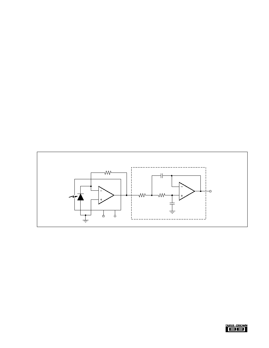
FIGURE 4. Rejecting Ambient Light.
This circuit also corrects output offset produced by input
bias current of a buffer used to extend bandwidth. A
Darlington transistor can be used for a bandwidth-enhancing
bootstrap buffer in this circuit without creating offset error.
NOISE PERFORMANCE
Noise performance of the OPT211 is shown in typical
curves for various feedback resistor values. This curve
specifies the total noise measured from 0.1Hz to the indi-
cated bandwidth. High frequency noise is reduced with the
bootstrap transistor buffer circuits shown in Figure 1. This
effect is shown on the typical curve.
Output noise of the OPT211 extends beyond the signal
bandwidth, especially for high feedback resistor values.
Signal-to-noise ratio can be improved by filtering the
OPT211's output to a bandwidth equal to the signal band-
width--see Figure 5.
AC COUPLING
Some applications are concerned only with sensing variation
in light intensity. Simple capacitive coupling at the OPT211's
output may be adequate. With large feedback resistors or
bright ambient light, however, the OPT211's output may
saturate. The circuit in Figure 4 can reject very bright
ambient light, yet provide high AC gain for best signal-to-
noise ratio. The output voltage is integrated and fed back to
the inverting input through R
3
. This drives the average (dc)
voltage at the output to zero. Application Bulletin AB-061
provides more details on this technique.
OPA177
C
1
0.1µF
C
2
0.1µF
R
2
1M
R
3
1M
R
1
1M
f
3dB
=
=16Hz
R
F
R
3
(2
R
2
C
2
)
2
3
6
OPT211
7
8
3
1
5
V
OUT
2
V
V+
R
F
= 10M
C
1
= C
2
R
1
= R
2
See Application Bulletin
AB-061 for details.
R
F
1M
C
F
(a)
(c)
(b)
+15V
15V
Q
1
2N5116
Bootstrap
Buffer
S
D
From
Pin 2
+15V
15V
Q
1
From
Pin 2
To Pin 7
R
1
6.8k
R
1
7.5k
OPT211
7
8
3
1
5
V
OUT
2
15V
+15V
OPA131
To Pin 7
2N6427
®
OPT211
9
Best signal-to-noise ratio is achieved by using the highest
practical feedback resistor. This comes with the trade-off of
decreased bandwidth.
The noise performance of a photodetector is sometimes
characterized by its noise effective power (NEP). This is the
radiant power which would produce an output signal equal
to the output noise level. NEP has the units of radiant
power (W). A NEP curve is provided.
LIGHT SOURCE POSITIONING
The OPT211 is 100% tested with a light source that uniformly
illuminates the full area of the integrated circuit, including
the op amp. Although all IC amplifiers are light-sensitive to
some degree, the OPT211 op amp circuitry is designed to
minimize this effect. Sensitive junctions are shielded with
metal, and differential stages are cross-coupled. Furthermore,
the photodiode area is very large relative to the op amp input
circuitry making these effects negligible.
If your light source is focused to a small area, be sure that
it is properly aimed to fall on the photodiode. If a narrowly
focused light source were to miss the photodiode area and
fall only on the op amp circuitry, the OPT211 would not
perform properly. The large (0.090 inch
x
0.090 inch)
photodiode area allows easy positioning of narrowly focused
light sources. The photodiode area is easily visible as it
appears very dark compared to the surrounding active
circuitry.
The incident angle of the light source also affects the
apparent sensitivity in uniform irradiance. For small incident
angles, the loss in sensitivity is simply due to the smaller
effective light gathering area of the photodiode (proportional
to the cosine of the angle). At a greater incident angle, light
is diffracted and scattered by the side of the package. These
effects are shown in the typical performance curve
"Responsivity vs Incident Angle."
LINEARITY PERFORMANCE
The photodiode inside the OPT211 is designed to be operated
in the photoconductive mode (V
DIODE
= 0V) for very linear
operation with radiant power throughout a wide range.
Nonlinearity remains below approximately 0.05% up to
100
µ
A photodiode current.
This very linear performance at high radiant power assumes
that the full photodiode area is uniformly illuminated. If the
light source is focused to a small area of the photodiode,
nonlinearity will occur at lower radiant power.
FIGURE 5. Low Pass Filter for Improved Signal-to-Noise Ratio.
OPA131
2.94k
21k
2.2nF
Sallen-Key Low Pass Filter Designed
Using Burr-Brown's Application Bulletin No. AB-034
470pF
f
3dB
= 20kHz
6
2
3
V
O
Sallen-Key
2-Pole Butterworth
OPT211
7
8
3
1
5
2
V
V+
R
F
=
10M