 | ÐлекÑÑоннÑй компоненÑ: REF10RM | СкаÑаÑÑ:  PDF PDF  ZIP ZIP |
Äîêóìåíòàöèÿ è îïèñàíèÿ www.docs.chipfind.ru
REF10
Precision
VOLTAGE REFERENCE
FEATURES
q
+10.00V OUTPUT
q
HIGH ACCURACY:
±
0.005V Untrimmed
q
VERY-LOW DRIFT: 1ppm/
°
C max
q
EXCELLENT STABILITY: 10ppm/1000hrs typ
q
LOW NOISE: 6
µ
Vp-p typ, 0.1Hz to 10Hz
q
WIDE SUPPLY RANGE: Up to 35V
DESCRIPTION
The REF10 is a precision voltage reference which
provides a +10.00V output. The drift is laser-trimmed
to 1ppm/
°
C max (KM grade) over the full specifica-
tion range. This is in contrast to some references
which guarantee drift over a limited portion of their
specification temperature range. The REF10 achieves
its precision without a heater. This results in low
quiescent current, fast warm-up, excellent stability,
and low noise.
The output can be adjusted with minimal effect on
drift or stability. Single supply operation over 13.5V
to 35V supply range and excellent overall specifica-
tions make the REF10 an ideal choice for the most
demanding applications such as precision system stan-
dard, D/A and A/D references, transducer excitation,
etc.
APPLICATIONS
q
PRECISION CALIBRATED VOLTAGE
STANDARD
q
TRANSDUCER EXCITATION
q
D/A AND A/D CONVERTER REFERENCE
q
PRECISION CURRENT REFERENCE
q
ACCURATE COMPARATOR THRESHOLD
REFERENCE
q
DIGITAL VOLTMETERS
q
TEST EQUIPMENT
R
2
7k
R
4
156k
R
3
2k
R
1
12k
D21
2
6
+V
CC
V
OUT
5
3
V
TRIM
V
Z
4 Common
70
60
50
40
30
20
10
0
10
20
30
40
50
60
70
0
Time (Hours)
Voltage Change (ppm)
TIME STABILITY
1k
2k
3k
®
International Airport Industrial Park · Mailing Address: PO Box 11400 · Tucson, AZ 85734 · Street Address: 6730 S. Tucson Blvd. · Tucson, AZ 85706
Tel: (520) 746-1111 · Twx: 910-952-1111 · Cable: BBRCORP · Telex: 066-6491 · FAX: (520) 889-1510 · Immediate Product Info: (800) 548-6132
©
1984 Burr-Brown Corporation
PDS-528B
Printed in U.S.A October, 1993
®
REF10
2
OUTPUT VOLTAGE
Initial
T
A
= +25
°
C
9.995
10.000
10.005
V
Trim Range
(1)
0.100
+0.250
V
vs Temperature
(2)
: KM
0
°
C to +70
°
C
1
ppm/
°
C
JM
0
°
C to +70
°
C
3
ppm/
°
C
SM
55
°
C to +125
°
C
3
ppm/
°
C
RM
55
°
C to +125
°
C
6
ppm/
°
C
vs Supply (line regulation)
V
CC
= 13.5 to 35V
0.001
0.002
%/V
vs Output Current (load regulation)
I
L
= 0 to
±
10mA
0.001
0.002
%/mA
vs Time
(3)
T
A
= +25
°
C
10
±
50
ppm/1000hr
NOISE
0.1Hz to 10Hz
6
25
µ
Vp-p
OUTPUT CURRENT
Source or Sink
±
10
mA
INPUT VOLTAGE RANGE
13.5
35
V
QUIESCENT CURRENT
I
OUT
= 0
4.5
6
mA
WARM-UP TIME
To 0.1%
10
µ
s
TEMPERATURE RANGE
Specification: JM, KM
0
+70
°
C
RM, SM
55
+125
°
C
Operating: JM, KM
25
+85
°
C
RM, SM
55
+125
°
C
Storage
65
+125
°
C
NOTES: (1) Trimming the offset voltage will affect the drift slightly. See Installation and Operating Instructions for details. (2) The "box method" is used to specify output
voltage drift vs temperature. See the Discussion of Performance section. (3) Sample tested with power applied continuously.
SPECIFICATIONS
ELECTRICAL
T
A
= +25
°
C, and
±
15VDC power supply, unless otherwise noted.
REF10JM, KM, RM, SM
PARAMETER
CONDITIONS
MIN
TYP
MAX
UNITS
ORDERING INFORMATION
TEMPERATURE
MAX DRIFT
MODEL
PACKAGE
RANGE
(ppm/
°
C)
REF10JM
Metal TO-99
0
°
C to +70
°
C
3
REF10KM
Metal TO-99
0
°
C to +70
°
C
1
REF10RM
Metal TO-99
55
°
C to +125
°
C
6
REF10SM
Metal TO-99
55
°
C to +125
°
C
3
Input Voltage ........................................................................................ 40V
Power Dissipation at +25
°
C ............................................................ 200mV
Operating Temperature
J, K .................................................................................. 25
°
C to +85
°
C
R, S ............................................................................... 55
°
C to +125
°
C
Storage Temperature Range .......................................... 65
°
C to +125
°
C
Lead Temperature (soldering, 10s) ................................................ +300
°
C
Short-Circuit Protection at +25
°
C
to Common or +15VDC ........................................................ Continuous
ABSOLUTE MAXIMUM RATINGS
PACKAGE INFORMATION
PACKAGE DRAWING
MODEL
PACKAGE
NUMBER
(1)
REF10JM
8-Pin Metal TO-99
001
REF10KM
8-Pin Metal TO-99
001
REF10RM
8-Pin Metal TO-99
001
REF10SM
8-Pin Metal TO-99
001
NOTE: (1) For detailed drawing and dimension table, please see end of data
sheet, or Appendix D of Burr-Brown IC Data Book.
PIN CONFIGURATION
Top View
NOTE: (1) Pin 3 is an unbuffered 6.3V output. Any load will affect the output
voltage and drift. A load of 1
µ
A on pin 3 will typically change the output voltage
by 50
µ
V and the drift by 0.1ppm/
°
C.
The information provided herein is believed to be reliable; however, BURR-BROWN assumes no responsibility for inaccuracies or omissions. BURR-BROWN
assumes no responsibility for the use of this information, and all use of such information shall be entirely at the user's own risk. Prices and specifications are subject
to change without notice. No patent rights or licenses to any of the circuits described herein are implied or granted to any third party. BURR-BROWN does not
authorize or warrant any BURR-BROWN product for use in life support devices and/or systems.
8
1
2
7
6
5
3
4
V
OUT
V
Z
(1)
TAB
Common
Trim
NC
+V
CC
NC = No Internal Connection.
NC
NC
®
REF10
3
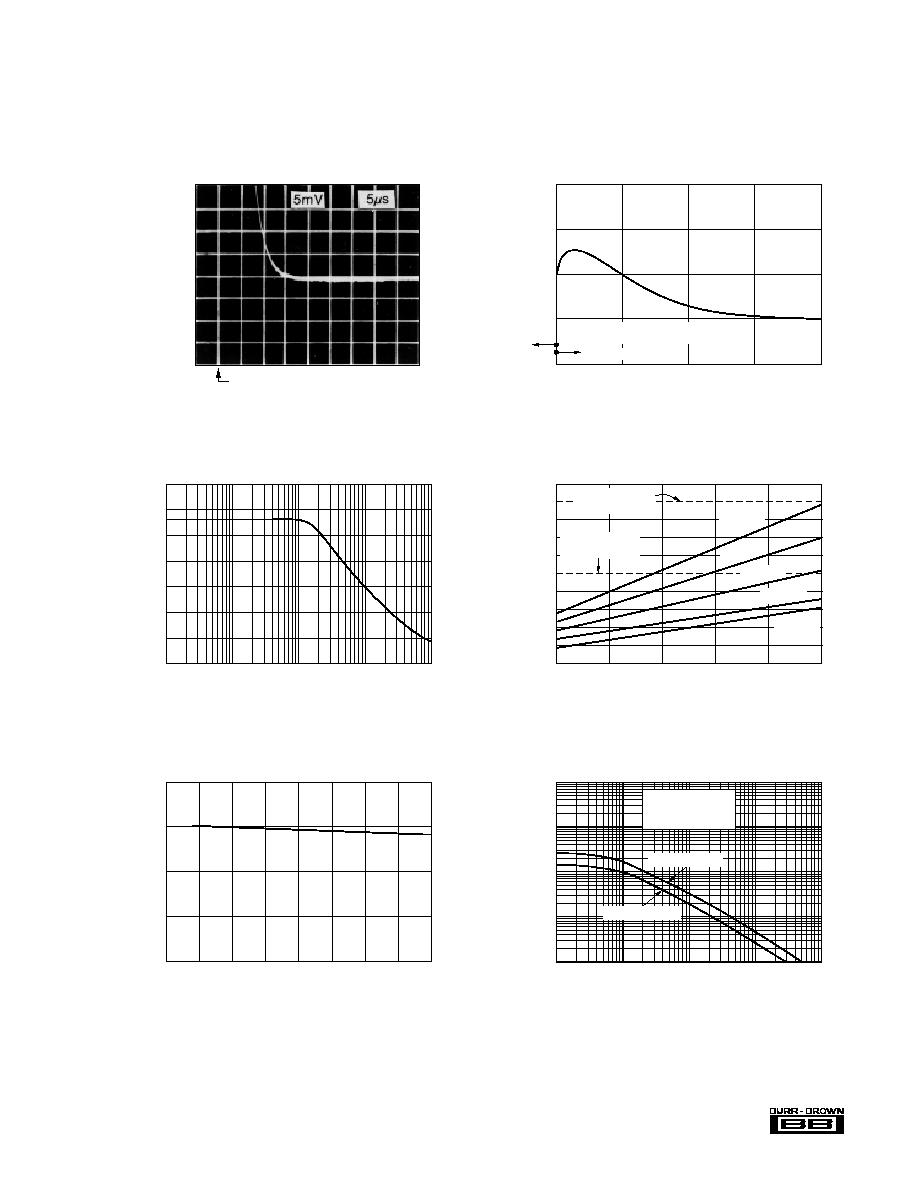
POWER TURN-ON RESPONSE
20
15
10
5
0
5
10
15
Power Turn-On
Error From Final Value (mV)
20
TYPICAL PERFORMANCE CURVES
T
A
= +25
°
C, and
±
15VDC power supply, unless otherwise noted.
400
200
0
200
400
T
A
=
+25°C
5
0
15
20
10
Time (µs)
Output Voltage
Cahnge (µV)
RESPONSE TO THERMAL SHOCK
T
A
= +70°C
Device Immersed in +70°C
Fluorinert Bath
100
90
80
70
60
50
40
30
100
0
10k
100k
1k
Frequency (Hz)
Power Supply Rejection (dB)
POWER SUPPLY REJECTION vs FREQUENCY
5
4
3
2
1
75
Temperature (°C)
Quiescent Current (mA)
QUIESCENT CURRENT vs TEMPERATURE
50
25
0
25
50
75
100
125
10k
1k
100
10
1
10k
R
S
(
)
Output Voltage Adjustment (mV)
OUTPUT VOLTAGE ADJUSTMENT vs R
S
100k
1M
10M
100M
See Optional Output
Voltage Fine Adjust,
Figure 4.
Voltage Increase
Voltage Decrease
100
80
60
40
20
0
2
0
6
8
4
Output Current (mA)
Junction Temperature Rise
Above Ambient (°C)
JUNCTION TEMPERATURE RISE
vs OUTPUT CURRENT
10
Max temp rise for
+85°C ambient
Max temp rise for
+125°C ambient
V
CC
= 35V
V
CC
= 25V
V
CC
= 20V
V
CC
= 15V
V
CC
= 30V
®
REF10
4
TYPICAL PERFORMANCE CURVES
(CONT)
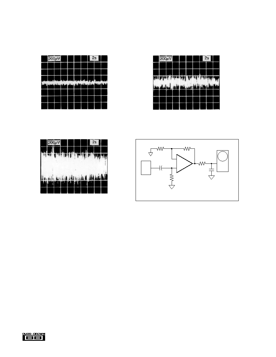
NOISE TEST CIRCUIT
T
A
= +25
°
C, and
±
15VDC power supply, unless otherwise noted.
+
OPA27
DUT
100µF
15.8k
20
2k
8K
2µF
Oscilloscope
Gain = 100V/V
f
3dB
= 0.1Hz and 10Hz
TYPICAL REF10 NOISE
Noise Voltage (
µ
V) (Referred to Input)
0
2
4
6
2
4
6
Low Frequency Noise
(see Noise Test Circuit)
TYPICAL BANDGAP REFERENCE NOISE
Noise Voltage (
µ
V) (Referred to Input)
0
2
4
6
2
4
6
Low Frequency Noise
(see Noise Test Circuit)
TYPICAL HEATED ZENER NOISE
Noise Voltage (
µ
V) (Referred to Input)
0
2
4
6
2
4
6
Low Frequency Noise
(see Noise Test Circuit)
®
REF10
5
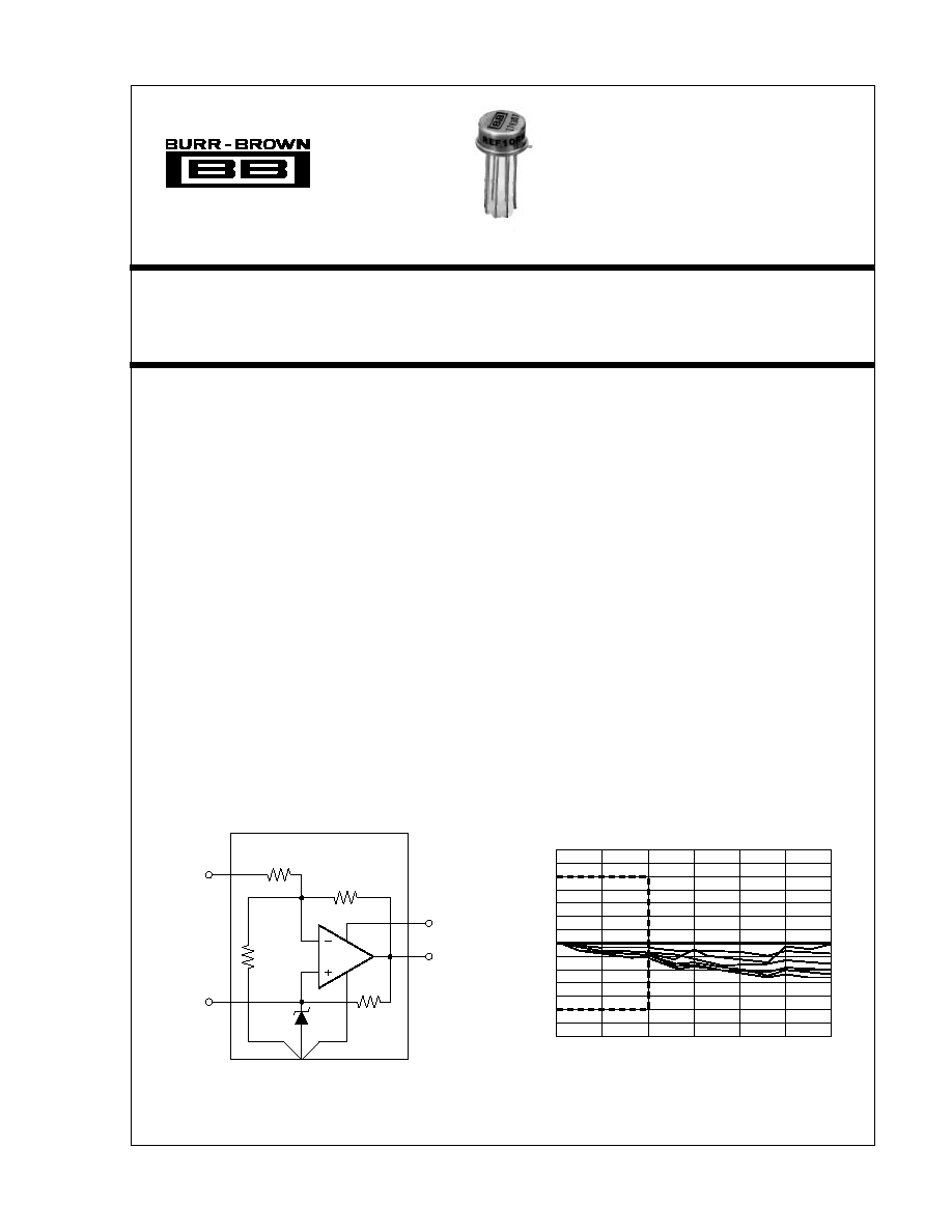
THEORY OF OPERATION
The following discussion refers to the diagram on the first
page.
In operation, approximately 6.3V is applied to the
noninverting input of op amp A
1
by zener diode D
Z1
. This
voltage is amplified by A
1
to produce the 10.00V output.
The gain is determined by R
1
and R
2
: G = (R
1
+ R
2
)/R
1
. R
1
and R
2
are actively laser-trimmed to produce an exact
10.00V output. The zener operating current is derived from
the regulated output voltage through R
3
. This feedback
arrangement provides closely regulated zener current. R
3
is
actively laser-trimmed to set the zener current to a level
which results in low drift at the output of A
1
. R
4
allows user-
trimming of the output voltage by providing for a small
external adjustment of amplifier gain. Since the TCR of R
4
closely matches the TCR of the gain setting resistors, the
voltage trim has minimal effect on the drift of the reference.
DISCUSSION OF
PERFORMANCE
The REF10 is designed for applications requiring a precision
voltage reference where both the initial value at room
temperature and the drift over temperature are of importance
to the user. Two basic methods of specifying voltage refer-
ence drift versus temperature are in common usage in the
industry--the "butterfly method" and the "box method."
The REF10 is specified with the more commonly used box
method. The "box" is formed by the high and low specifica-
tion temperatures and a diagonal, the slope of which is equal
to the maximum specified drift.
For the REF10, each J and K unit is tested at temperatures
of 0
°
C, +25
°
C, +50
°
C, and +70
°
C. Each R and S unit is
tested at 55
°
C, 25
°
C, 0
°
C, +25
°
C, +50
°
C, +75
°
C, +100
°
C
and +125
°
C. The minimum and maximum test voltages
must meet this condition:
This assures the user that the variations of output voltage
that occur as the temperature changes within the specifica-
tion range, T
LOW
to T
HIGH
, will be contained within a box
whose diagonal has a slope equal to the maximum specified
drift. Since the shape of the actual drift curve is not known,
the vertical position of the box is not exactly known either.
It is, however, bounded by V
UPPER BOUND
and V
LOWER BOUND
(see
Figure 1).
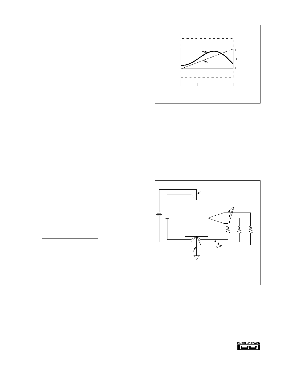
Figure 1 uses the REF10KM as an example. It has a drift
specification of 1ppm/
°
C maximum and a specification
temperature range of 0
°
C to +70
°
C. The "box" height (V
1
to
V
2
) is 700
µ
V, and upper bound and lower bound voltages
are a maximum of 700
µ
V away from the voltage at +25
°
C.
FIGURE 1. REF10KM Output Voltage Drift.
INSTALLATION AND
OPERATING INSTRUCTIONS
BASIC CIRCUIT CONNECTION
Figure 2 shows the proper connection of the REF10. To
achieve the specified performance, pay careful attention to
layout. A low resistance star configuration will reduce volt-
age errors, noise pickup, and noise coupled from the power
supply. Commons should be connected as indicated being
sure to minimize interconnection resistances.
REF10
2
6
4
1µF
Tantalum
+
R
L1
R
L2
R
L3
(2)
(2)
(1)
(1)
V
CC
FIGURE 2. REF10 Installation.
NOTES: (1) Lead resistances here of up to a few
have negligible effect on
performance. (2) A resistance of 0.1
in series with these leads will cause
a 1mV error when the load current is at its maximum of 10mA. This results
in a 0.01% error of 10V.
OPTIONAL OUTPUT VOLTAGE ADJUSTMENT
Optional output voltage adjustment circuits are shown in
Figures 3 and 4. Trimming the output voltage will change
the voltage drift by approximately 0.01ppm/
°
C per mV of
trimmed voltage. In the circuit in Figure 3, any mismatch in
TCR between the two sections of the potentiometer will also
V
UPPER BOUND
+10.0007
V
1
V
NOMINAL
+10.0000
V
2
+9.9993
0
25
70
Output Voltage (V)
Temperature (°C)
700µV
Worst-case
V
OUT
for REF10KM
V
UPPER BOUND
(T
HIGH
)
Typical Drift
Diagonal
1ppm/°C for REF10KM
(T
LOW
)
V
OUT MAX
V
OUT MIN
(
)
/ 10V
T
HIGH
T
LOW
X
10
6
Drift
Specification