REF3112
REF3120
REF3125
REF3130
REF3133
REF3140
SBVS046A ≠ DECEMBER 2003 ≠ REVISED JANUARY 2004
www.ti.com
DESCRIPTION
The REF31xx is a family of precision, low power, low dropout,
series voltage references available in the tiny SOT23-3 pack-
age.
The REF31xx's small size and low power consumption
(100
µ
A typ) make it ideal for portable and battery-powered
applications. The REF31xx does not require a load capacitor,
but is stable with any capacitive load and can sink/source up
to 10mA of output current.
Unloaded, the REF31xx can be operated on supplies down
to 5mV above the output voltage. All models are specified for
the wide temperature range of ≠40
∞
C to +125
∞
C.
FEATURES
q
MicroSIZE PACKAGE: SOT23-3
q
LOW DROPOUT: 5mV
q
HIGH OUTPUT CURRENT:
±
10mA
q
HIGH ACCURACY: 0.2% max
q
LOW I
Q
: 115
µ
A max
q
EXCELLENT SPECIFIED DRIFT PERFORMANCE:
15ppm/
∞
C (max) from 0
∞
C to +70
∞
C
20ppm/
∞
C (max) from ≠40
∞
C to +125
∞
C
Copyright © 2003-2004, Texas Instruments Incorporated
15ppm/
∞
C Max, 100
µ
A, SOT23-3
SERIES VOLTAGE REFERENCE
Please be aware that an important notice concerning availability, standard warranty, and use in critical applications of
Texas Instruments semiconductor products and disclaimers thereto appears at the end of this data sheet.
APPLICATIONS
q
PORTABLE, BATTERY-POWERED EQUIPMENT
q
DATA ACQUISITION SYSTEMS
q
MEDICAL EQUIPMENT
q
HAND-HELD TEST EQUIPMENT
PRODUCT
VOLTAGE (V)
REF3112
1.25
REF3120
2.048
REF3125
2.5
REF3130
3.0
REF3133
3.3
REF3140
4.096
1
IN
2
OUT
3
GND
REF3112
REF3120
REF3125
REF3130
REF3133
REF3140
SOT23-3
PRODUCTION DATA information is current as of publication date.
Products conform to specifications per the terms of Texas Instruments
standard warranty. Production processing does not necessarily include
testing of all parameters.
All trademarks are the property of their respective owners.

REF3112, 3120, 3125, 3130, 3133, 3140
2
SBVS046A
www.ti.com
ABSOLUTE MAXIMUM RATINGS
(1)
Supply Voltage, V+ to V≠ ................................................................... 7.0V
Output Short-Circuit ................................................................. Continuous
Operating Temperature .................................................. ≠55
∞
C to +135
∞
C
Storage Temperature ..................................................... ≠65
∞
C to +150
∞
C
Junction Temperature .................................................................... +150
∞
C
Lead Temperature (soldering, 10s) ............................................... +300
∞
C
NOTES: (1) Stresses above these ratings may cause permanent damage.
Exposure to absolute maximum conditions for extended periods may degrade
device reliability. These are stress ratings only, and functional operation of the
device at these, or any other conditions beyond those specified, is not implied.
SPECIFIED
PACKAGE
TEMPERATURE
PACKAGE
ORDERING
TRANSPORT
PRODUCT
PACKAGE-LEAD
DESIGNATOR
RANGE
MARKING
NUMBER
MEDIA, QUANTITY
REF3112
SO T23-3
DBZ
≠40
∞
C to +125
∞
C
R31A
REF3112AIDBZT
Tape and Reel, 250
"
"
"
"
"
REF3112AIDBZR
Tape and Reel, 3000
REF3120
SOT23-3
DBZ
≠40
∞
C to +125
∞
C
R31B
REF3120AIDBZT
Tape and Reel, 250
"
"
"
"
"
REF3120AIDBZR
Tape and Reel, 3000
REF3125
SOT23-3
DBZ
≠40
∞
C to +125
∞
C
R31C
REF3125AIDBZT
Tape and Reel, 250
"
"
"
"
"
REF3125AIDBZR
Tape and Reel, 3000
REF3130
SOT23-3
DBZ
≠40
∞
C to +125
∞
C
R31E
REF3130AIDBZT
Tape and Reel, 250
"
"
"
"
"
REF3130AIDBZR
Tape and Reel, 3000
REF3133
SOT23-3
DBZ
≠40
∞
C to +125
∞
C
R31F
REF3133AIDBZT
Tape and Reel, 250
"
"
"
"
"
REF3133AIDBZR
Tape and Reel, 3000
REF3140
SOT23-3
DBZ
≠40
∞
C to +125
∞
C
R31D
REF3140AIDBZT
Tape and Reel, 250
"
"
"
"
"
REF3140AIDBZR
Tape and Reel, 3000
NOTES: (1) For the most current package and ordering information, see the Package Option Addendum located at the end of this data sheet.
PACKAGE/ORDERING INFORMATION
(1)
ELECTRICAL CHARACTERISTICS
Boldface limits apply over the specified temperature range, T
A
= ≠40
∞
C to +125
∞
C.
At T
A
= +25
∞
C, I
LOAD
= 0mA, V
IN
= 5V, unless otherwise noted.
REF31xx
PARAMETER
CONDITIONS
MIN
TYP
MAX
UNITS
ELECTROSTATIC
DISCHARGE SENSITIVITY
This integrated circuit can be damaged by ESD. Texas Instru-
ments recommends that all integrated circuits be handled with
appropriate precautions. Failure to observe proper handling
and installation procedures can cause damage.
ESD damage can range from subtle performance degradation
to complete device failure. Precision integrated circuits may be
more susceptible to damage because very small parametric
changes could cause the device not to meet its published
specifications.
REF3112
(1)
- 1.25V
OUTPUT VOLTAGE
V
OUT
1.2475
1.25
1.2525
V
Initial Accuracy
≠0.2
0.2
%
NOISE
Output Voltage Noise
f = 0.1Hz to 10Hz
17
µ
V
PP
Voltage Noise
f = 10Hz to 10kHz
24
µ
Vrms
REF3120 ≠ 2.048
OUTPUT VOLTAGE
V
OUT
2.0439
2.048
2.0521
V
Initial Accuracy
≠0.2
0.2
%
NOISE
Output Voltage Noise
f = 0.1Hz to 10Hz
27
µ
V
PP
Voltage Noise
f = 10Hz to 10kHz
39
µ
Vrms
REF3125 ≠ 2.5V
OUTPUT VOLTAGE
V
OUT
2.4950
2.50
2.5050
V
Initial Accuracy
≠0.2
0.2
%
NOISE
Output Voltage Noise
f = 0.1Hz to 10Hz
33
µ
V
PP
Voltage Noise
f = 10Hz to 10kHz
48
µ
Vrms

REF3112, 3120, 3125, 3130, 3133, 3140
3
SBVS046A
www.ti.com
ELECTRICAL CHARACTERISTICS
Boldface limits apply over the specified temperature range, T
A
= ≠40
∞
C to +125
∞
C.
At T
A
= +25
∞
C, I
LOAD
= 0mA, V
IN
= +5V, unless otherwise noted.
REF31xx
PARAMETER
CONDITIONS
MIN
TYP
MAX
UNITS
REF3130 ≠ 3.0V
OUTPUT VOLTAGE
V
OUT
2.9940
3.0
3.0060
V
Initial Accuracy
≠0.2
0.2
%
NOISE
Output Voltage Noise
f = 0.1Hz to 10Hz
39
µ
V
PP
Voltage Noise
f = 10Hz to 10kHz
57
µ
Vrms
REF3133 ≠ 3.3V
OUTPUT VOLTAGE
V
OUT
3.2934
3.30
3.3066
V
Initial Accuracy
≠0.2
0.2
%
NOISE
Output Voltage Noise
f = 0.1Hz to 10Hz
43
µ
V
PP
Voltage Noise
f = 10Hz to 10kHz
63
µ
Vrms
REF3140 ≠ 4.096V
OUTPUT VOLTAGE
V
OUT
4.0878
4.096
4.1042
V
Initial Accuracy
≠0.2
0.2
%
NOISE
Output Voltage Noise
f = 0.1Hz to 10Hz
53
µ
V
PP
Voltage Noise
f = 10Hz to 10kHz
78
µ
Vrms
REF3112, REF3120, REF3125, REF3130, REF3133, REF3140
OUTPUT VOLTAGE TEMP DRIFT
(2)
dV
OUT
/dT
0
∞
C
T
A
+70
∞
C
5
15
ppm/
∞
C
≠40
∞
C
T
A
+125
∞
C
10
20
ppm/
∞
C
LONG-TERM STABILITY
0-1000h
70
ppm
LINE REGULATION
V
REF
+ 0.05
(1)
V
IN
5.5V
20
65
ppm/V
LOAD REGULATION
(3)
dV
OUT
/dI
LOAD
Sourcing
0mA < I
LOAD
< 10mA,
10
30
µ
V/mA
V
IN
= V
REF
+ 250mV
(1)
Sinking
≠10mA < I
LOAD
< 0mA,
20
50
µ
V/mA
V
IN
= V
REF
+ 100mV
(1)
THERMAL HYSTERESIS
(4)
dT
First Cycle
100
ppm
Additional Cycles
25
ppm
DROPOUT VOLTAGE
(1)
V
IN
≠ V
OUT
5
50
mV
OUTPUT CURRENT
I
LOAD
≠10
10
mA
SHORT-CIRCUIT CURRENT
I
SC
Sourcing
50
mA
Sinking
40
mA
TURN-ON SETTLING TIME
to 0.1% at V
IN
= +5V with C
L
= 0
400
µ
s
POWER SUPPLY
I
L
= 0
Voltage
V
S
V
REF
+ 0.05
(1)
5.5
V
Quiescent Current
I
Q
100
115
µ
A
Over Temperature
115
135
µ
A
TEMPERATURE RANGE
Specified Range
≠40
+125
∞
C
Operating Range
≠55
+135
∞
C
Storage Range
≠65
+150
∞
C
Thermal Resistance
SOT23-3 Surface-Mount
JA
336
∞
C/W
NOTES: (1) Minimum supply voltage for REF3112 is 1.8V.
(2) Box Method used to determine temperature drift.
(3) Typical value of load regulation reflects measurements using force and sense contacts, see section
Load Regulation.
(4) Thermal hysteresis is explained in more detail in Applications Information section of data sheet.
(5) For I
L
> 0, see Typical Characteristic curves.

REF3112, 3120, 3125, 3130, 3133, 3140
4
SBVS046A
www.ti.com
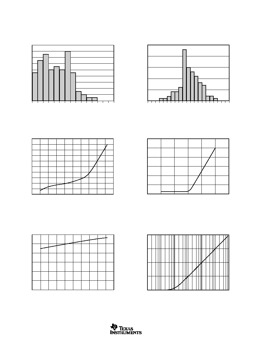
TYPICAL CHARACTERISTICS
At T
A
= +25
∞
C, V
IN
= +5V power supply, REF3125 is used for typical characteristics, unless otherwise noted.
TEMPERATURE DRIFT (0
∞
C to +70
∞
C)
18
16
14
12
10
8
6
4
2
0
Percentage of Units
1
0
Drift (ppm/
∞
C)
2
3
4
5
6
8
9
10 11 12 13 14 15 16
TEMPERATURE DRIFT (≠40
∞
C to +125
∞
C)
25
20
15
10
5
0
Percentage of Units
1
0
Drift (ppm/
∞
C)
2 3 4 5 6 7 8 9 10 11 12 13 14 15 16 17 18 19 20 21
OUTPUT VOLTAGE vs TEMPERATURE
0.16
0.14
0.12
0.10
0.08
0.06
0.04
0.02
0
-
0.02
-
0.04
Output Drift (%)
-
60
-
40
-
20
0
40
20
60
80
100
120
140
Temperature (
∞
C)
DROPOUT VOLTAGE vs LOAD CURRENT
120
100
80
60
40
20
0
Dropout Voltage (mV)
≠15
≠10
≠5
0
5
10
15
Load Current (mA)
QUIESCENT CURRENT vs TEMPERATURE
120
100
80
60
40
20
0
Quiescent Current (
µ
A)
≠60
≠40
≠20
0
20
40
60
100
120
80
140
Temperature (
∞
C)
OUTPUT IMPEDANCE vs FREQUENCY
100
10
1
0.1
0.01
Output Resistance (
)
1
10
100
1k
100k
10k
1M
Frequency (Hz)

REF3112, 3120, 3125, 3130, 3133, 3140
5
SBVS046A
www.ti.com
TYPICAL CHARACTERISTICS
(Cont.)
At T
A
= +25
∞
C, V
IN
= +5V power supply, REF3125 is used for typical characteristics, unless otherwise noted.
PSRR vs FREQUENCY
90
80
70
60
50
40
30
20
10
0
Power-Supply Rejection Ratio (dB)
1
10
100
1k
10k
100k
Frequency (Hz)
OUTPUT vs SUPPLY
2.505
2.504
2.503
2.502
2.501
2.500
2.499
2.498
Output (V)
2.0
2.5
3.0
3.5
4.0
4.5
5.5
6.0
5.0
6.5
Supply (V)
+125
∞
C
+25
∞
C
-
40
∞
C
OUTPUT VOLTAGE vs LOAD CURRENT
2.505
2.504
2.503
2.502
2.501
2.500
2.499
2.498
2.497
Output Voltage (V)
≠15
≠10
≠5
0
5
10
15
Load Current (mA)
+125
∞
C
+25
∞
C
-
40
∞
C
STEP RESPONSE, C
L
= 0, 5V STARTUP
100
µ
s/div
V
IN
V
OUT
5V/div
1V/div
0.1Hz TO 10Hz NOISE
10
µ
V/div
400ms/div
REF3112 LONG TERM STABILITY
20
0
≠20
≠40
≠60
≠80
≠100
≠120
Drift (ppm)
0
100
200
300 400
500
600
700
800 900 1000
Time (Hrs)

REF3112, 3120, 3125, 3130, 3133, 3140
6
SBVS046A
www.ti.com
TYPICAL CHARACTERISTICS
(Cont.)
At T
A
= +25
∞
C, V
IN
= +5V power supply, REF3125 is used for typical characteristics, unless otherwise noted.
LINE TRANSIENT
C
L
= 0pF
20mV/div
500mV/div
20
µ
s/div
V
IN
V
OUT
LINE TRANSIENT
C
L
= 10
µ
F
100
µ
s/div
20mV/div
500mV/div
V
IN
V
OUT
LOAD TRANSIENT
C
L
= 0pF,
±
10mA OUTPUT PULSE
40
µ
s/div
200mV/div
V
OUT
+10mA
≠10mA
+10mA
V
IN
40
µ
s/div
50mV/div
LOAD TRANSIENT
C
L
= 1
µ
F,
±
10mA OUTPUT PULSE
V
OUT
+10mA
+10mA
≠10mA
V
IN
40
µ
s/div
100mV/div
LOAD TRANSIENT
C
L
= 0pF,
±
1mA OUTPUT PULSE
V
OUT
+1mA
≠1mA
+1mA
V
IN
40
µ
s/div
20mV/div
LOAD TRANSIENT
C
L
= 1
µ
F,
±
1mA OUTPUT PULSE
V
OUT
+1mA
≠1mA
+1mA
V
IN

REF3112, 3120, 3125, 3130, 3133, 3140
7
SBVS046A
www.ti.com
THEORY OF OPERATION
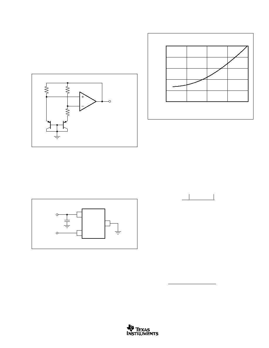
The REF31xx is a family of series, CMOS, precision bandgap
voltage references. The basic bandgap topology is shown in
Figure 1. Transistors Q
1
and Q
2
are biased such that the
current density of Q
1
is greater than that of Q
2
. The difference
of the two base-emitter voltages, Vbe
1
≠ Vbe
2
, has a positive
temperature coefficient and is forced across resistor R
1
. This
voltage is gained up and added to the base-emitter voltage
of Q
2
, which has a negative temperature coefficient. The
resulting output voltage is virtually independent of temperature.
100
µ
A, and the maximum quiescent current over temperature
is just 135
µ
A. The quiescent current typically changes less
than 2
µ
A over the entire supply range, as shown in Figure 3.
1
3
REF31xx
2
0.47
µ
F
V
IN
V
OUT
FIGURE 1. Simplified Schematic of Bandgap Reference.
FIGURE 2. Typical Connections for Operating REF31xx.
FIGURE 3. Supply Current vs Supply Voltage.
R
1
Q
2
Q
1
I
N
+
Vbe
1
≠
+
Vbe
2
≠
V
BANDGAP
APPLICATION INFORMATION
The REF31xx does not require a load capacitor and is stable
with any capacitive load. Figure 2 shows typical connections
required for operation of the REF31xx. A supply bypass
capacitor of 0.47
µ
F is recommended.
SUPPLY VOLTAGE
The REF31xx family of references features an extremely low
dropout voltage. With the exception of the REF3112, which
has a minimum supply requirement of 1.8V, these references
can be operated with a supply of only 5mV above the output
voltage in an unloaded condition. For loaded conditions, a
typical dropout voltage versus load is shown in the typical
curves.
The REF31xx features a low quiescent current, which is
extremely stable over changes in both temperature and
supply. The typical room temperature quiescent current is
Supply voltages below the specified levels can cause the
REF31xx to momentarily draw currents greater than the
typical quiescent current. This can be prevented by using a
power supply with a fast rising edge and low output impedance.
THERMAL HYSTERESIS
Thermal hysteresis for the REF31xx is defined as the change
in output voltage after operating the device at 25
∞
C, cycling
the device through the specified temperature range, and
returning to 25
∞
C. It can be expressed as:
V
abs V
V
V
ppm
HYST
PRE
POST
NOM
=
∑
(
)
≠
10
6
Where: V
HYST
=
Thermal hysteresis
V
PRE
= Output voltage measured at 25
∞
C pre-
temperature cycling
V
POST
= Output voltage measured after the device
has been cycled through the specified temperature
range of ≠40
∞
C to +125
∞
C and returned to 25
∞
C.
TEMPERATURE DRIFT
The REF31xx is designed to exhibit minimal drift error, defined
as the change in output voltage over varying temperature. The
drift is calculated using the "box" method which is described by
the following equation:
V
V
V
TemperatureRange
ppm
OUTMAX
OUTMIN
OUT
≠
∑
∑
10
6
The REF31xx features a typical drift coefficient of 5ppm from
0
∞
C to 70
∞
C--the primary temperature range for many
applications. For the industrial temperature range of ≠40
∞
C to
125
∞
C, the REF31xx family drift increases to a typical value of
10ppm.
QUIESCENT CURRENT vs POWER SUPPLY
100.5
100.0
99.5
99.0
98.5
98.0
Quiescent Current (
µ
A)
1.5
Power Supply (V)
2.5
3.5
4.5
5.5

REF3112, 3120, 3125, 3130, 3133, 3140
8
SBVS046A
www.ti.com
NOISE PERFORMANCE
Typical 0.1Hz to 10Hz voltage noise can be seen in the
Typical Characteristic Curve,
0.1 to 10Hz Voltage Noise. The
noise voltage of the REF31xx increases with output voltage
and operating temperature. Additional filtering may be used
to improve output noise levels, although care should be
taken to ensure the output impedance does not degrade the
AC performance.
LONG-TERM STABILITY
Long-term stability refers to the change of the output voltage
of a reference over a period of months or years. This effect
lessens as time progresses, as is shown by the long-term
stability curves. The typical drift value for the REF31xx is
70ppm from 0-1000 hours. This parameter is characterized
by measuring 30 units at regular intervals for a period of 1000
hours.
LOAD REGULATION
Load regulation is defined as the change in output voltage
due to changes in load current. The load regulation of the
REF31xx is measured using force and sense contacts as
pictured in Figure 4. The force and sense lines reduce the
impact of contact and trace resistance, resulting in accurate
measurement of the load regulation contributed solely by the
REF31xx. For applications requiring improved load regula-
tion, force and sense lines should be used.
Output Pin
Meter
V
OUT
+
≠
Sense Line
Force Line
Load
I
L
Contact and
Trace Resistance
FIGURE 4. Accurate Load Regulation of REF31xx.
APPLICATION CIRCUITS
Negative Reference Voltage
For applications requiring a negative and positive reference
voltage, the REF31xx and OPA703 can be used to provide
a dual supply reference from a
±
5V supply. Figure 5 shows
the REF3125 used to provide a
±
2.5V supply reference
voltage. The low drift performance of the REF31xx
complement the low offset voltage and low drift of the
OPA703 to provide an accurate solution for split-supply
applications.
OPA703
REF3125
+5V
≠5V
+5V
10k
10k
+2.5V
≠2.5V
FIGURE 5. REF3125 Combined with OPA703 to Create
Positive and Negative Reference Voltages.
DATA ACQUISITION
Data acquisition systems often require stable voltage
references to maintain accuracy. The REF31xx family features
stability and a wide range of voltages suitable for most micro-
controllers and data converters. Figure 6, Figure 7, and
Figure 8 show basic data acquisition systems.

REF3112, 3120, 3125, 3130, 3133, 3140
9
SBVS046A
www.ti.com
FIGURE 6. Basic Data Acquisition System 1.
FIGURE 7. Basic Data Acquisition System 2.
ADS7822
V
CC
CS
D
OUT
DCLOCK
V
REF
+In
≠In
GND
+
+
5
1
µ
F to 10
µ
F
1
µ
F to
10
µ
F
3.3V
0.1
µ
F
V
IN
V+
V
S
Microcontroller
REF3133
GND
ADS8324
V
CC
CS
D
OUT
DCLOCK
V
REF
+In
≠In
GND
+
+
5
1
µ
F to 10
µ
F
1
µ
F to 10
µ
F
0.1
µ
F
0V to 1.25V
Microcontroller
2.5V Supply
REF3112
GND
V
IN
2.5V
V
OUT
= 1.25V
V
S
FIGURE 8. REF3140 Provides an Accurate Reference for Driving the ADS8381.
ADS8381
REF3140
10
1k
1k
10
0.1
µ
F
1
µ
F
22
µ
F
V
OUT
=
4.096V
V
REF
5V
500
0.22
µ
F
THS4031
+5V
≠5V
V
IN
6800pF

MECHANICAL DATA
MPDS108 ≠ AUGUST 2001
POST OFFICE BOX 655303
∑
DALLAS, TEXAS 75265
DBZ (R-PDSO-G3)
PLASTIC SMALL-OUTLINE
0,55 REF
4203227/A 08/01
3,04
2,80
2,05
1,78
1,03
0,89
0,60
0,45
2,64
2,10
1,40
1,20
0,51
0,37
1,12
0,89
0,100
0,013
0,180
0,085
NOTES: A. All linear dimensions are in millimeters.
B. This drawing is subject to change without notice.
C. Dimensions are inclusive of plating.
D. Dimensions are exclusive of mold flash and metal burr.

IMPORTANT NOTICE
Texas Instruments Incorporated and its subsidiaries (TI) reserve the right to make corrections, modifications,
enhancements, improvements, and other changes to its products and services at any time and to discontinue
any product or service without notice. Customers should obtain the latest relevant information before placing
orders and should verify that such information is current and complete. All products are sold subject to TI's terms
and conditions of sale supplied at the time of order acknowledgment.
TI warrants performance of its hardware products to the specifications applicable at the time of sale in
accordance with TI's standard warranty. Testing and other quality control techniques are used to the extent TI
deems necessary to support this warranty. Except where mandated by government requirements, testing of all
parameters of each product is not necessarily performed.
TI assumes no liability for applications assistance or customer product design. Customers are responsible for
their products and applications using TI components. To minimize the risks associated with customer products
and applications, customers should provide adequate design and operating safeguards.
TI does not warrant or represent that any license, either express or implied, is granted under any TI patent right,
copyright, mask work right, or other TI intellectual property right relating to any combination, machine, or process
in which TI products or services are used. Information published by TI regarding third-party products or services
does not constitute a license from TI to use such products or services or a warranty or endorsement thereof.
Use of such information may require a license from a third party under the patents or other intellectual property
of the third party, or a license from TI under the patents or other intellectual property of TI.
Reproduction of information in TI data books or data sheets is permissible only if reproduction is without
alteration and is accompanied by all associated warranties, conditions, limitations, and notices. Reproduction
of this information with alteration is an unfair and deceptive business practice. TI is not responsible or liable for
such altered documentation.
Resale of TI products or services with statements different from or beyond the parameters stated by TI for that
product or service voids all express and any implied warranties for the associated TI product or service and
is an unfair and deceptive business practice. TI is not responsible or liable for any such statements.
Following are URLs where you can obtain information on other Texas Instruments products and application
solutions:
Products
Applications
Amplifiers
amplifier.ti.com
Audio
www.ti.com/audio
Data Converters
dataconverter.ti.com
Automotive
www.ti.com/automotive
DSP
dsp.ti.com
Broadband
www.ti.com/broadband
Interface
interface.ti.com
Digital Control
www.ti.com/digitalcontrol
Logic
logic.ti.com
Military
www.ti.com/military
Power Mgmt
power.ti.com
Optical Networking
www.ti.com/opticalnetwork
Microcontrollers
microcontroller.ti.com
Security
www.ti.com/security
Telephony
www.ti.com/telephony
Video & Imaging
www.ti.com/video
Wireless
www.ti.com/wireless
Mailing Address:
Texas Instruments
Post Office Box 655303 Dallas, Texas 75265
Copyright
2004, Texas Instruments Incorporated


