Document Outline
- FEATURES
- APPLICATIONS
- DESCRIPTION
- ABSOLUTE MAXIMUM RATINGS(
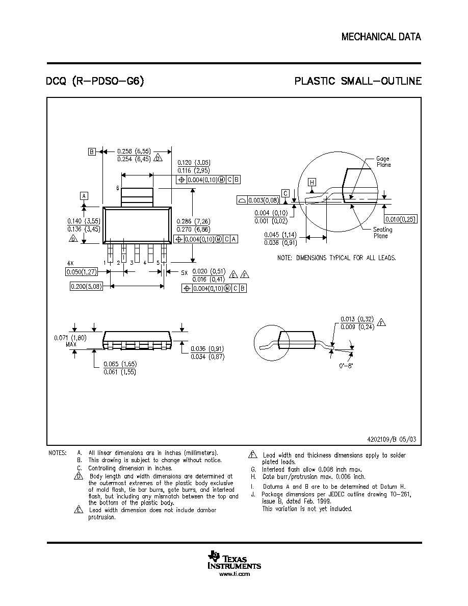
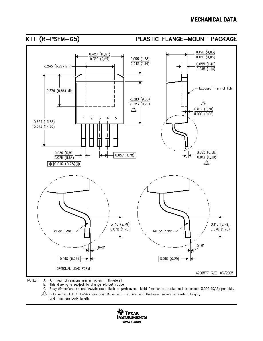
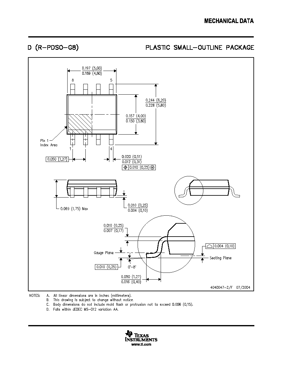
- PACKAGE/ORDERING INFORMATION(
- ELECTRICAL CHARACTERISTICS
- PIN CONFIGURATIONS
- TYPICAL CHARACTERISTICS
- BASIC OPERATION
- INTERNAL CURRENT LIMIT
- ENABLE
- ERROR\ FLAG
- OUTPUT NOISE
- DROP-OUT VOLTAGE
- TRANSIENT RESPONSE
- THERMAL PROTECTION
- POWER DISSIPATION
- REGULATOR MOUNTING

DMOS
500mA Low-Dropout Regulator
FEATURES
q
NEW DMOS TOPOLOGY:
Ultra Low Dropout Voltage:
115mV Typ at 500mA and 3.3V Output
Output Capacitor NOT Required for Stability
q
FAST TRANSIENT RESPONSE
q
VERY LOW NOISE: 33
µ
Vrms
q
HIGH ACCURACY:
±
2% max
q
HIGH EFFICIENCY:
I
GND
= 1mA at I
OUT
= 500mA
Not Enabled: I
GND
= 0.5
µ
A
q
2.5V, 2.7V, 3.0V, 3.3V, 5.0V, AND ADJUSTABLE
OUTPUT VERSIONS
q
FOLDBACK CURRENT LIMIT
q
THERMAL PROTECTION
q
OUTPUT VOLTAGE ERROR INDICATOR
(1)
q
SMALL SURFACE-MOUNT PACKAGES:
SOT223-5, DDPAK-5, SO-8
APPLICATIONS
q
PORTABLE COMMUNICATION DEVICES
q
BATTERY-POWERED EQUIPMENT
q
PERSONAL DIGITAL ASSISTANTS
q
MODEMS
q
BAR-CODE SCANNERS
q
BACKUP POWER SUPPLIES
DESCRIPTION
The REG103 is a family of low-noise, low-dropout, linear
regulators with low ground pin current. Its new DMOS
topology provides significant improvement over previous
designs, including low-dropout voltage (only 115mV typ at
full load), and better transient performance. In addition, no
output capacitor is required for stability, unlike conventional
low-dropout regulators that are difficult to compensate and
require expensive low ESR capacitors greater than 1
µ
F.
Typical ground pin current is only 1mA (at I
OUT
= 500mA)
and drops to 0.5
µ
A in not enabled mode. Unlike regulators
with PNP pass devices, quiescent current remains relatively
constant over load variations and under dropout conditions.
The REG103 has very low output noise (typically 33
µ
Vrms
for V
OUT
= 3.3V with C
NR
= 0.01
µ
F), making it ideal for use
in portable communications equipment. On-chip trimming
results in high output voltage accuracy. Accuracy is main-
tained over temperature, line, and load variations. Key
parameters are tested over the specified temperature range
(≠40
∞
C to +85
∞
C).
The SO-8 version of the REG103 has an ERROR pin that
provides a power good flag, indicating the regulator is in
regulation. The REG103 is well protected--internal cir-
cuitry provides a current limit that protects the load from
damage. Thermal protection circuitry keeps the chip from
being damaged by excessive temperature. In addition to the
SO-8 package, the REG103 is also available in the DDPAK
and the SOT223-5.
REG103
(Fixed Voltage
Versions)
ENABLE
Gnd
0.1
µ
F
C
OUT
(2)
+
+
V
OUT
V
IN
NR
NR = Noise Reduction
NOTE: (1) SO-8 Package Only. (2) Optional.
ERROR
(1)
ERROR
1)
REG103-A
Gnd
ENABLE
0.1
µ
F
+
C
OUT
(2)
+
V
OUT
V
IN
R
2
R
1
Adj
REG103
REG1
03
REG1
03
REG103
SBVS010B ≠ JANUARY 2000 ≠ REVISED FEBRUARY 2004
www.ti.com
PRODUCTION DATA information is current as of publication date.
Products conform to specifications per the terms of Texas Instruments
standard warranty. Production processing does not necessarily include
testing of all parameters.
Copyright © 2000-2004, Texas Instruments Incorporated
Please be aware that an important notice concerning availability, standard warranty, and use in critical applications of
Texas Instruments semiconductor products and disclaimers thereto appears at the end of this data sheet.
All trademarks are the property of their respective owners.
REG103
2
SBVS010B
ABSOLUTE MAXIMUM RATINGS
(1)
Supply Input Voltage, V
IN
....................................................... ≠0.3V to 16V
Enable Input ............................................................................ ≠0.3V to V
IN
Error Flag Output ..................................................................... ≠0.3V to 6V
Error Flag Current ............................................................................... 2mA
Output Short-Circuit Duration ...................................................... Indefinite
Operating Temperature Range ....................................... ≠55
∞
C to +125
∞
C
Storage Temperature Range .......................................... ≠65
∞
C to +150
∞
C
Junction Temperature ..................................................... ≠55
∞
C to +150
∞
C
Lead Temperature (soldering, 3s, SO-8, SOT, and DDPAK) ............... +240
∞
C
NOTE: (1) Stresses above these ratings may cause permanent damage.
Exposure to absolute maximum conditions for extended periods may degrade
device reliability.
ELECTROSTATIC
DISCHARGE SENSITIVITY
This integrated circuit can be damaged by ESD. Texas
Instruments recommends that all integrated circuits be handled
with appropriate precautions. Failure to observe proper han-
dling and installation procedures can cause damage.
ESD damage can range from subtle performance degrada-
tion to complete device failure. Precision integrated circuits
may be more susceptible to damage because very small
parametric changes could cause the device not to meet its
published specifications.
SPECIFIED
PACKAGE
TEMPERATURE
PACKAGE
ORDERING
TRANSPORT
PRODUCT
PACKAGE-LEAD
DESIGNATOR
RANGE
MARKING
NUMBER
MEDIA, QUANTITY
5V Output
REG103FA-5
DDPAK-5
KTT
≠40
∞
C to +85
∞
C
REG103FA-5.0
REG103FA-5KTTT
Tape and Reel, 50
"
"
"
"
"
REG103FA-5/500
Tape and Reel, 500
REG103UA-5
SO-8
D
≠40
∞
C to +85
∞
C
REG103U50
REG103UA-5
Rails, 100
"
"
"
"
"
REG103UA-5/2K5
Tape and Reel, 2500
REG103GA-5
SOT223-5
DCQ
≠40
∞
C to +85
∞
C
R103G50
REG103GA-5
Rails, 78
"
"
"
"
"
REG103GA-5/2K5
Tape and Reel, 2500
3.3V Output
REG103FA-3.3
DDPAK-5
KTT
≠40
∞
C to +85
∞
C
REG103FA-3.3
REG103FA-3.3KTTT
Tape and Reel, 50
"
"
"
"
"
REG103FA-3.3/500
Tape and Reel, 500
REG103UA-3.3
SO-8
D
≠40
∞
C to +85
∞
C
REG103UA4
REG103UA-3.3
Rails, 100
"
"
"
"
"
REG103UA-3.3/2K5
Tape and Reel, 2500
REG103GA-3.3
SOT223-5
DCQ
≠40
∞
C to +85
∞
C
R103G33
REG103GA-3.3
Rails, 78
"
"
"
"
"
REG103GA-3.3/2K5
Tape and Reel, 2500
3.0V Output
REG103FA-3
DDPAK-5
KTT
≠40
∞
C to +85
∞
C
REG103FA-3.0
REG103FA-3KTTT
Tape and Reel, 50
"
"
"
"
"
REG103FA-3/500
Tape and Reel, 500
REG103UA-3
SO-8
D
≠40
∞
C to +85
∞
C
REG103U30
REG103UA-3
Rails, 100
"
"
"
"
"
REG103UA-3/2K5
Tape and Reel, 2500
REG103GA-3
SOT223-5
DCQ
≠40
∞
C to +85
∞
C
R103G30
REG103GA-3
Rails, 78
"
"
"
"
"
REG103GA-3/2K5
Tape and Reel, 2500
2.7V Output
REG103FA-2.7
DDPAK-5
KTT
≠40
∞
C to +85
∞
C
REG103FA-2.7
REG103FA-2.7KTTT
Tape and Reel, 50
"
"
"
"
"
REG103FA-2.7/500
Tape and Reel, 500
REG103UA-2.7
SO-8
D
≠40
∞
C to +85
∞
C
REG103U27
REG103UA-2.7
Rails, 100
"
"
"
"
"
REG103UA-2.7/2K5
Tape and Reel, 2500
REG103GA-2.7
SOT223-5
DCQ
≠40
∞
C to +85
∞
C
R103G27
REG103GA-2.7
Rails, 78
"
"
"
"
"
REG103GA-2.7/2K5
Tape and Reel, 2500
2.5V Output
REG103FA-2.5
DDPAK-5
KTT
≠40
∞
C to +85
∞
C
REG103FA-2.5
REG103FA-2.5KTTT
Tape and Reel, 50
"
"
"
"
"
REG103FA-2.5/500
Tape and Reel, 500
REG103UA-2.5
SO-8
D
≠40
∞
C to +85
∞
C
REG103U25
REG103UA-2.5
Rails, 100
"
"
"
"
"
REG103UA-2.5/2K5
Tape and Reel, 2500
REG103GA-2.5
SOT223-5
DCQ
≠40
∞
C to +85
∞
C
R103G25
REG103GA-2.5
Rails, 78
"
"
"
"
"
REG103GA-2.5/2K5
Tape and Reel, 2500
Adjustable Output
REG103FA-A
DDPAK-5
KTT
≠40
∞
C to +85
∞
C
REG103FA-A
REG103FA-AKTTT
Tape and Reel, 50
"
"
"
"
"
REG103FA-A/500
Tape and Reel, 500
REG103UA-A
SO-8
D
≠40
∞
C to +85
∞
C
REG103UA
REG103UA-A
Rails, 100
"
"
"
"
"
REG103UA-A/2K5
Tape and Reel, 2500
REG103GA-A
SOT223-5
DCQ
≠40
∞
C to +85
∞
C
R103GA
REG103GA-A
Rails, 78
"
"
"
"
"
REG103GA-A/2K5
Tape and Reel, 2500
NOTE: (1) For the most current package and ordering information, refer to our web site at www.ti.com.
PACKAGE/ORDERING INFORMATION
(1)
REG103
3
SBVS010B
ELECTRICAL CHARACTERISTICS
Boldface limits apply over the specified temperature range, T
J
= ≠40
∞
C to +85
∞
C.
At T
J
= +25
∞
C, V
IN
= V
OUT
+ 1V (V
OUT
= 3.0V for REG103-A), V
ENABLE
= 2V, I
OUT
= 10mA, C
NR
= 0.01
µ
F, and C
OUT
= 0.1
µ
F
(1)
, unless otherwise noted.
REG103GA, UA, FA
PARAMETER
CONDITION
MIN
TYP
MAX
UNITS
OUTPUT VOLTAGE
Output Voltage Range
V
OUT
REG103-2.5
2.5
V
REG103-2.7
2.7
V
REG103-3.0
3.0
V
REG103-3.3
3.3
V
REG103-5
5
V
REG103-A
V
REF
5.5
V
Reference Voltage
V
REF
1.295
V
Adjust Pin Current
I
ADJ
0.2
1
µ
A
Accuracy
±
0.5
±
2
%
T
J
= ≠40
∞
C to +85
∞
C
±
2.8
%
vs Temperature
dV
OUT
/dT
T
J
= ≠40
∞
C to +85
∞
C
70
ppm/
∞
C
vs Line and Load
I
OUT
= 10mA to 500mA, V
IN
= (V
OUT
+ 0.7V) to 15V
±
0.5
±
2.5
%
T
J
= ≠40
∞
C to +85
∞
C
V
IN
= (V
OUT
+ 0.9V) to 15V
±
3.5
%
DC DROPOUT VOLTAGE
(2, 3)
V
DROP
I
OUT
= 10mA
3
25
mV
For all models except 5V
I
OUT
= 500mA
115
200
mV
For 5V model
I
OUT
= 500mA
160
250
mV
For all models except 5V
I
OUT
= 500mA
230
mV
T
J
= ≠40
∞
C to +85
∞
C
For 5V models
I
OUT
= 500mA
280
mV
T
J
= ≠40
∞
C to +85
∞
C
VOLTAGE NOISE
f = 10Hz to 100kHz
V
n
Without C
NR
(all models)
C
NR
= 0, C
OUT
= 0
30
µ
Vrms/V ∑ V
OUT
µ
Vrms
With C
NR
(all fixed voltage models)
C
NR
= 0.01
µ
F, C
OUT
= 10
µ
F
10
µ
Vrms/V ∑ V
OUT
µ
Vrms
OUTPUT CURRENT
Current Limit
(4)
I
CL
550
700
950
mA
T
J
= ≠40
∞
C to +85
∞
C
500
1000
mA
RIPPLE REJECTION
f = 120Hz
65
dB
ENABLE CONTROL
V
ENABLE
HIGH (output enabled)
V
ENABLE
2
V
IN
V
V
ENABLE
LOW (output disabled)
≠0.2
0.5
V
I
ENABLE
HIGH (output enabled)
I
ENABLE
V
ENABLE
= 2V to V
IN
, V
IN
= 2.1V to 6.5
(5)
1
100
nA
I
ENABLE
LOW (output disabled)
V
ENABLE
= 0V to 0.5V
2
100
nA
Output Disable Time
50
µ
s
Output Enable Soft Start Time
1.5
ms
ERROR FLAG
(6)
Current, Logic HIGH (open drain)--Normal Operation
V
IN
= V
ERROR
= V
OUT
+ 1V
0.1
10
µ
A
Voltage, Logic LOW--On Error
Sinking 500
µ
A
0.2
0.4
V
THERMAL SHUTDOWN
Junction Temperature
Shutdown
150
∞
C
Reset from Shutdown
130
∞
C
GROUND PIN CURRENT
Ground Pin Current
I
GND
I
OUT
= 10mA
0.5
0.7
mA
I
OUT
= 500mA
1
1.3
mA
ENABLE Pin LOW
V
ENABLE
0.5V
0.5
µ
A
INPUT VOLTAGE
V
IN
Operating Input Voltage Range
(7)
2.1
15
V
Specified Input Voltage Range
V
IN
> 2.7V
V
OUT
+ 0.7
15
V
T
J
= ≠40
∞
C to +85
∞
C
V
IN
> 2.9V
V
OUT
+ 0.9
15
V
TEMPERATURE RANGE
Specified Range
T
J
≠40
+85
∞
C
Operating Range
≠55
+125
∞
C
Storage Range
≠65
+150
∞
C
Thermal Resistance
DDPAK-5 Surface-Mount
JC
Junction-to-Case
4
∞
C/W
SO-8 Surface-Mount
JA
Junction-to-Ambient
150
∞
C/W
SOT223-5 Surface-Mount
JC
Junction-to-Case
15
∞
C/W
NOTES: (1) The REG103 does not require a minimum output capacitor for stability. However, transient response can be improved with proper capacitor selection.
(2) Dropout voltage is defined as the input voltage minus the output voltage that produces a 2% change in the output voltage from the value at V
IN
= V
OUT
+ 1V at fixed load.
(3) Not applicable for V
OUT
less than 2.7V. (4) Current limit is the output current that produces a 10% change in output voltage from V
IN
= V
OUT
+ 1V and I
OUT
= 10mA.
(4) For V
IN
> 6.5V, see typical characteristic "V
ENABLE
vs I
ENABLE
." (6) Logic low indicates out-of-regulation condition by approximately 10%, or thermal shutdown. (7) The
REG103 no longer regulates when V
IN
< V
OUT
+ V
DROP (MAX)
. In drop-out or when the input voltage is between 2.7V and 2.1V, the impedance from V
IN
to V
OUT
is typically
less than 1
at T
J
= +25
∞
C. See typical characteristic.
REG103
4
SBVS010B
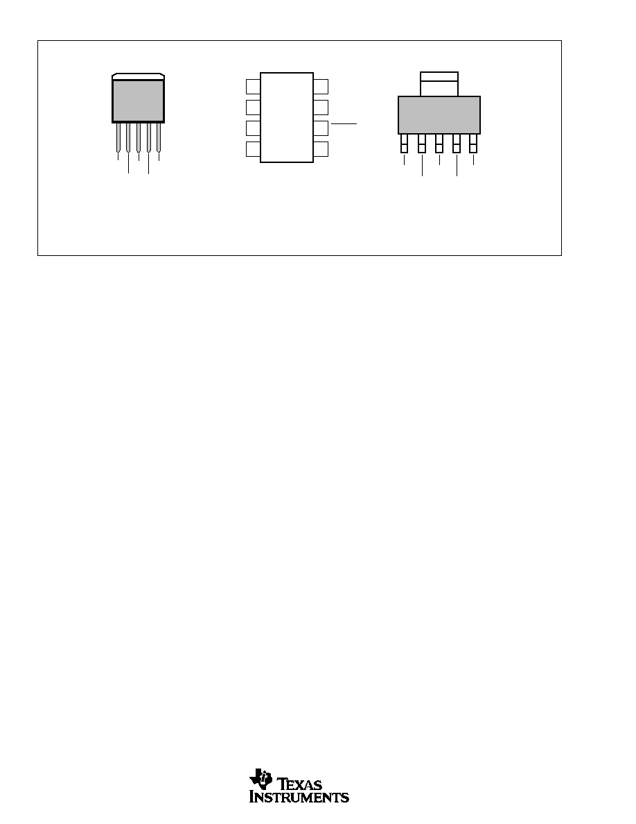
PIN CONFIGURATIONS
Top View
V
OUT
V
OUT
NR/Adjust
(1)
GND
V
IN
V
IN
ERROR
ENABLE
SO-8
1
2
3
4
8
7
6
5
NOTE: (1) For REG103A-A: voltage setting resistor pin.
All other models: noise reduction capacitor pin.
GND
ENABLE
V
IN
NR/Adjust
(1)
V
O
1 2 3 4 5
DDPAK-5
SOT223-5
(U Package)
(F Package)
(G Package)
Tab is GND
Tab is GND
ENABLE
NR/Adjust
(1)
GND
V
IN
1
2
3
4
5
V
OUT

REG103
5
SBVS010B
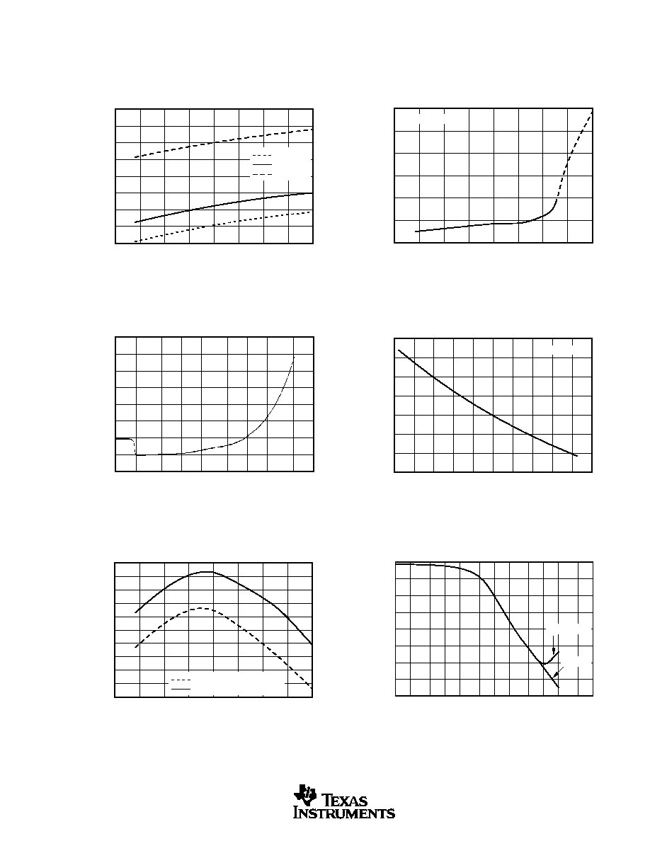
TYPICAL CHARACTERISTICS
For all models, at T
J
= +25
∞
C and V
ENABLE
= 2V, unless otherwise noted.
100
0
200
300
400
500
0.5
0
≠0.5
≠1.0
≠1.5
Output Voltage Change (%)
I
OUT
(mA)
OUTPUT VOLTAGE CHANGE vs I
OUT
(V
IN
= V
OUT
+ 1V, Output Voltage % Change
Refered to I
OUT
= 10mA at +25
∞
C)
= ≠55
∞
C
= +25
∞
C
= +125
∞
C
100
0
200
300
400
500
180
160
140
120
100
80
60
40
20
0
DC Dropout Voltage (mV)
Output Current (mA)
DC DROPOUT VOLTAGE vs OUTPUT CURRENT
= ≠55
∞
C
= +25
∞
C
= +125
∞
C
≠75
≠25
≠50
25
0
50
75
100
125
0.1
0.5
0
≠0.5
≠1
≠1.5
Output Voltage Change (%)
Temperature (
∞
C)
OUTPUT VOLTAGE vs TEMPERATURE
(Output Voltage % Change Referred to
I
OUT
= 10mA at +25
∞
C)
= 10mA
= 100mA
= 500mA
≠75
≠25
≠50
25
0
50
75
100
125
160
120
80
40
0
DC Dropout Voltage (mV)
Temperature (
∞
C)
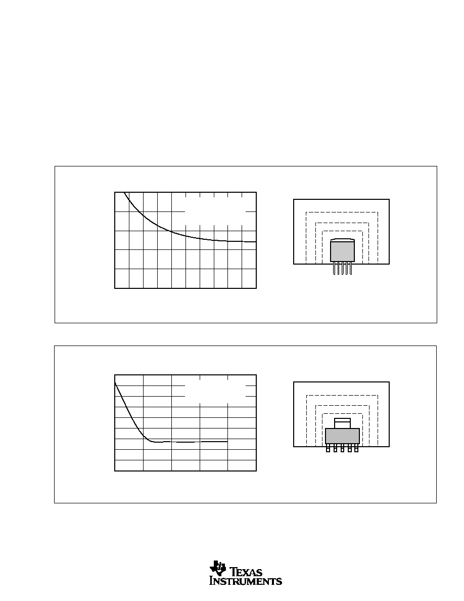
DC DROPOUT VOLTAGE vs TEMPERATURE
= 10mA
= 100mA
= 500mA
≠75
≠25
≠50
25
0
50
75
100
125
0.5
0.4
0.3
0.2
0.1
0
Output Voltage Change (%)
Temperature (
∞
C)
LINE REGULATION vs TEMPERATURE
(V
IN
= V
OUT
+ 1V to V
IN
= 15V )
= 10mA
= 100mA
0
2
4
6
10
8
0.5
0
≠0.5
≠1.0
≠1.5
Output Voltage Change (%)
Input Voltage Above V
OUT
OUTPUT VOLTAGE CHANGE vs V
IN
(Output Voltage % Change Refered
to V
IN
= V
OUT
+ 1V at I
OUT
= 10mA)
= 10mA
= 100mA
= 500mA
REG103
6
SBVS010B
TYPICAL CHARACTERISTICS
(Cont.)
For all models, at T
J
= +25
∞
C and V
ENABLE
= 2V, unless otherwise noted.
≠75
≠25
≠50
25
0
50
100
75
125
0.5
0.4
0.3
0.2
0.1
0
Output Voltage Change (%)
Temperature (
∞
C)
LOAD REGULATION vs TEMPERATURE
(V
IN
= V
OUT
+ 1V and 10mA < I
OUT
< 500mA)
10
100
1000
10000
100,000
10
1
0.1
0.01
Noise Density (
µ
V/
Hz)
Frequency (Hz)
OUTPUT NOISE DENSITY
C
NR
= 0
C
OUT
= 0
C
NR
= 0.01
µ
F
C
OUT
= 10
µ
F
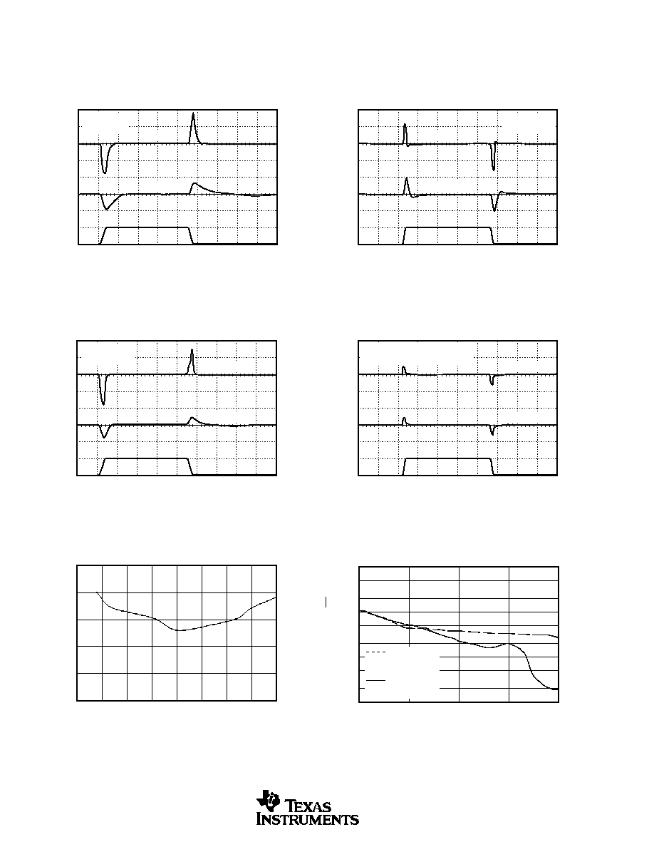
LOAD TRANSIENT RESPONSE
200mV/div
200mV/div
500mA
10mA
I
OUT
V
OUT
V
OUT
10
µ
s/div
REG103-3.3
V
IN
= 4.3V
C
OUT
= 0
C
OUT
= 10
µ
F
LINE TRANSIENT RESPONSE
50mV/div
50mV/div
6V
5V
V
IN
V
OUT
V
OUT
50
µ
s/div
REG103-3.3
Load = 100mA
C
OUT
= 0
C
OUT
= 10
µ
F
LOAD TRANSIENT RESPONSE
200mV/div
200mV/div
500mA
10mA
I
OUT
V
OUT
V
OUT
10
µ
s/div
REG103-Adj.
V
OUT
= 3.3V, V
IN
= 4.3V, C
FB
= 0.01
µ
F
C
OUT
= 0
C
OUT
= 10
µ
F
LINE TRANSIENT RESPONSE
50mV/div
50mV/div
6V
5V
V
IN
V
OUT
V
OUT
50
µ
s/div
REG103-Adj.
V
OUT
= 3.3V, C
FB
= 0.01
µ
F, I
OUT
= 100mA
C
OUT
= 0
C
OUT
= 10
µ
F
REG103
7
SBVS010B
TYPICAL CHARACTERISTICS
(Cont.)
For all models, at T
J
= +25
∞
C and V
ENABLE
= 2V, unless otherwise noted.
≠75
≠25
≠50
25
0
50
75
100
125
1.2
1.1
1
0.9
0.8
0.7
0.6
0.5
0.4
I
GND
(mA)
Temperature (
∞
C)
GROUND PIN CURRENT vs TEMPERATURE
= 10mA
= 100mA
= 500mA
≠75
≠50
≠25
0
25
50
75
100
125
3
2.5
2
1.5
1
0.5
0
I
GND
(
µ
A)
Temperature (
∞
C)
GROUND PIN CURRENT, NOT ENABLED
vs TEMPERATURE
V
ENABLE
= 0V
≠75
≠50
≠25
0
25
50
75
100
125
730
720
710
700
690
680
670
660
650
640
630
Current Limit (mA)
Temperature (
∞
C)
CURRENT LIMIT vs TEMPERATURE
V
OUT
= V
OUT-NOMINAL
∑ 0.90
V
OUT
= 1V
≠20
≠40
0
40
80
120
≠60
20
60
100
140
0.28
0.26
0.24
0.22
0.20
0.18
0.16
0.14
Adjust Pin Current (
µ
A)
Temperature (
∞
C)
I
ADJUST
vs TEMPERATURE
REG103-A
1
10
100
1000
1.2
1.1
1
0.9
0.8
0.7
0.6
0.5
0.4
I
GND
(mA)
I
OUT
(mA)
GROUND PIN CURRENT vs I
OUT
10
100
1000
10000
100000
70
60
50
40
30
20
Ripple Rejection (dB)
Frequency (Hz)
RIPPLE REJECTION vs FREQUENCY
C
OUT
= 10
µ
F
C
OUT
= 0

REG103
8
SBVS010B
TYPICAL CHARACTERISTICS
(Cont.)
For all models, at T
J
= +25
∞
C and V
ENABLE
= 2V, unless otherwise noted.
OUTPUT VOLTAGE DRIFT HISTOGRAM
Percent of Units (%)
V
OUT
Drift (ppm/
∞
C)
40
45
50
55
60
65
70
75
80
85
90
45
40
35
30
25
20
15
10
5
0
OUTPUT VOLTAGE ACCURACY HISTOGRAM
Percent of Units (%)
Error (%)
≠1
≠0.8 ≠0.6 ≠0.4 ≠0.2
0
0.2
0.4
0.6
0.8
1
60
50
40
30
20
10
0
0
100
200
300
400
500
75
70
65
60
55
50
45
40
Ripple Rejection (dB)
Load Current (mA)
RIPPLE REJECTION vs I
OUT
V
RIPPLE
= 3Vp-p, f = 120Hz
SOFT START
V
OUT
V
ENABLE
1V/div
2V
0
250
µ
s/div
No Load
R
LOAD
= 6.8
OUTPUT DISABLE TIME
V
OUT
V
ENABLE
1V/div
2V
0
10
µ
s/div
No Load
R
LOAD
= 6.8
R
LOAD
= 330
REG103
9
SBVS010B
BASIC OPERATION
The REG103 series is a family of LDO (Low Drop-Out)
linear regulators. The family includes five fixed output
versions (2.5V to 5.0V) and an adjustable output version. An
internal DMOS power device provides low dropout regula-
tion with near constant ground pin current (largely indepen-
dent of load and drop-out conditions) and very fast line and
load transient response. All versions include internal current
limit and thermal shutdown circuitry.
Figure 1 shows the basic circuit connections for the fixed
voltage models. Figure 2 gives the connections for the
adjustable output version (REG103A) and example resistor
values for some commonly used output voltages. Values for
other voltages can be calculated from the equation shown in
Figure 2. The SO-8 package provides two pins each for V
IN
and V
OUT
. Both sets of pins MUST be used and connected
adjacent to the device.
FIGURE 1. Fixed Voltage Nominal Circuit for REG103.
REG103
ENABLE
V
OUT
C
OUT
V
IN
0.1
µ
F
C
NR
0.01
µ
F
ERROR
Gnd
NR
In
Out
Optional
None of the versions require an output capacitor for regula-
tor stability. The REG103 will accept any output capacitor
type less than 1
µ
F. For capacitance values larger than 1
µ
F,
the effective ESR should be greater than 0.1
. This mini-
mum ESR value includes parasitics such as printed circuit
board traces, solder joints, and sockets. A minimum 0.1
µ
F
low ESR capacitor connected to the input supply voltage is
recommended.
INTERNAL CURRENT LIMIT
The REG103 internal current limit has a typical value of
700mA. A fold-back feature limits the short-circuit current
to a typical short-circuit value of 40mA. This circuit will
protect the regulator from damage under all load conditions.
A typical characteristic of V
OUT
versus I
OUT
is given in
Figure 3a.
Care should be taken in high current applications to avoid
ground currents flowing in the circuit board traces causing
voltage drops between points on the circuit. If voltage drops
occur on the circuit board ground that causes the load ground
voltage to be much lower than the ground voltage seen by
the ground pin on the REG103, the foldback current may
approach zero and the REG103 may not start up. In these
types of applications, a large value resistor can be placed
between V
IN
and V
OUT
to help "boost" up the output of the
REG103 during start-up, see Figure 3b. The value for the
"boost" resistor should be chosen so that the current through
the "boost" resistor is less than the minimum load current:
R
BOOST
> (V
IN
≠ V
OUT
)/I
LOAD
. Typically, a good value for a
"boost" resistor is 5k
.
FIGURE 2. Adjustable Voltage Circuit for REG103A.
V
OUT
= (1 + R
1
/R
2
) ∑ 1.295V
Pin numbers for SO-8 package.
REG103
V
IN
0.1
µ
F
4
7
8
Gnd
V
OUT
R
1
C
FB
0.01
µ
F
C
OUT
Adj
R
2
I
ADJ
Load
1
2
3
6
5
ERROR
ENABLE
To reduce current through divider, increase resistor
values (see table at right).
As the impedance of the resistor divider increases,
I
ADJ
(~200nA) may introduce an error.
C
FB
improves noise and transient response.
V
OUT
(V)
R
1
(
)
(1)
R
2
(
)
(1)
1.295
Short
Open
2.5
12.1k
13k
1.21k
1.3k
3
16.9k
13k
1.69k
1.3k
3.3
20k
13k
2.0k
1.3k
5
37.4k
13k
3.74k
1.3k
NOTE: (1) Resistors are standard 1% values.
EXAMPLE RESISTOR VALUES
Optional
REG103
10
SBVS010B
0
2
4
6
8
10
12
14
16
100
10
1
0.1
0.01
0.001
Enable Current (
µ
A)
Enable Voltage
FIGURE 5. ENABLE Pin Current versus Applied Voltage.
REG103
ERROR
+5V
10k
Pull-up
3
ENABLE
SO-8 Package
Only
6
Open
Drain
µ
P
FIGURE 6. ERROR Pin Typical Fault-Monitoring Circuit.
ENABLE
The ENABLE pin allows the regulator to be turned on and
off. This pin is active HIGH and compatible with standard
TTL-CMOS levels. Inputs below 0.5V (max) turn the regu-
lator off and all circuitry is disabled. Under this condition,
ground pin current drops to approximately 0.5
µ
A. When not
used, the ENABLE pin may be connected to V
IN
.
Internal to the part, the ENABLE pin is connected to an
input resistor-zener diode circuit, as shown in Figure 4,
creating a nonlinear input impedance. The ENABLE Pin
Current versus Applied Voltage relationship is shown in
Figure 5. When the ENABLE pin is connected to a voltage
greater than 10V, a series resistor may be used to limit the
current.
ENABLE
V
Z
= 10V
175k
FIGURE 4. ENABLE Pin Equivalent Input Circuit.
FIGURE 3. Foldback Current Limit and Boost Circuit.
0
100
200
300
400
500
600
700
800
3.5
3
2.5
2
1.5
1
0.5
0
Output Voltage (V)
Output Current (mA)
REG103
V
IN
0.1
µ
F
Gnd
R
BOOST
V
OUT
+
0.1
µ
F
(1)
Load
+
(1) Optional.
(a) Foldback Current Limit of the REG103-3.3 at 25
∞
C.
(b) Foldback Current Boost Circuit.
ERROR FLAG
The error indication pin, only available on the SO-8 package
version, provides a fault indication out-of-regulation condi-
tion. During a fault condition, ERROR is pulled LOW by an
open drain output device. The pin voltage, in the fault state,
is typically less than 0.2V at 500
µ
A.
A fault condition is indicated when the output voltage differs
(either above or below) from the specified value by approxi-
mately 10%. Figure 6 shows a typical fault-monitoring
application.
OUTPUT NOISE
A precision band-gap reference is used for the internal
reference voltage, V
REF
, for the REG103. This reference is
the dominant noise source within the REG103. It generates
approximately 45
µ
Vrms in the 10Hz to 100kHz bandwidth
at the reference output. The regulator control loop gains up
the reference noise, so that the noise voltage of the regulator
is approximately given by:
V
Vrms
R
R
R
Vrms
V
V
N
OUT
REF
= µ
+
= µ
∑
45
2
45
1
2
REG103
11
SBVS010B
Since the value of V
REF
is 1.295V, this relationship reduces to:
V
Vrms
V
V
N
OUT
=
µ
∑
35
Connecting a capacitor, C
NR
, from the Noise-Reduction
(NR) pin to ground, can reduce the output noise voltage.
Adding C
NR
, as shown in Figure 7, forms a low-pass filter
for the voltage reference. For C
NR
= 10nF, the total noise in
the 10Hz to 100kHz bandwidth is reduced by approximately
a factor of 3.5, as shown in Figure 8.
FIGURE 7. Block Diagram.
Over Current
Over Temp
Protection
V
REF
(1.295V)
Low Noise
Charge Pump
DMOS
Output
R
1
NOTE: R
1
and R
2
are internal
on fixed output versions.
V
OUT
Adj
(Adjustable
Versions)
R
2
NR
(fixed output
versions only)
ENABLE
REG103
V
IN
ERROR
C
NR
(optional)
FIGURE 8. Output Noise versus Noise-Reduction Capacitor.
0.001
0.01
0.1
1
45
35
25
Output Noise Voltage
(
µ
V
RMS
10Hz - 100kHz)
C
NR
(
µ
F)
C
OUT
= 0
C
OUT
= 10
µ
F
FIGURE 9. Output Noise Density on Adjustable Versions.
100
10
1000
10000
100000
10.0
1.0
0.1
nV/
Hz
Frequency
C
OUT
= 0, C
FB
= 0
C
OUT
= 0, C
FB
= 0.01
µ
F
C
OUT
= 10
µ
F, C
FB
= 0.01
µ
F
The REG103 adjustable version does not have the noise-
reduction pin available, however, the adjust pin is the sum-
ming junction of the error amplifier. A capacitor, C
FB
,
connected from the output to the adjust pin will reduce both
the output noise and the peak error from a load transient.
Figure 9 shows improved output noise performance for two
capacitor combinations.
The REG103 utilizes an internal charge pump to develop an
internal supply voltage sufficient to drive the gate of the
DMOS pass element above V
IN
. The charge-pump switch-
ing noise (nominal switching frequency = 2MHz) is not
measurable at the output of the regulator.
DROP-OUT VOLTAGE
The REG103 uses an N-channel DMOS as the "pass"
element. When the input voltage is within a few hundred
millivolts of the output voltage, the DMOS device behaves
like a resistor. Therefore, for low values of V
IN
to V
OUT
, the
regulator's input-to-output resistance is the Rds
ON
of the
DMOS pass element (typically 230m
)
. For static (DC)
loads, the REG103 will typically maintain regulation down
to V
IN
to V
OUT
voltage drop of 115mV at full-rated output
current. In Figure 10, the bottom line (DC dropout) shows
the minimum V
IN
to V
OUT
voltage drop required to prevent
drop-out under DC load conditions.

REG103
12
SBVS010B
FIGURE 11. Maximum Power Dissipation versus Ambient
Temperature for the Various Packages and
PCB Heat Sink Configurations.
6
5
4
3
2
1
0
Power Dissipation (Watts)
0
25
50
75
100
150
125
Ambient Temperature (
∞
C)
CONDITIONS
#1
#2
#3
#4
#5
CONDITION
PACKAGE
PCB AREA
THETA J-A
1
DDPAK
4in
2
Top Side Only
27
∞
C/W
2
SOT-223
4in
2
Top Side Only
53
∞
C/W
3
DDPAK
None
65
∞
C/W
4
SOT-223
0.5in
2
Top Side Only
110
∞
C/W
5
SO-8
None
150
∞
C/W
For large step changes in load current, the REG103 requires
a larger voltage drop across it to avoid degraded transient
response. The boundary of this "transient drop-out" region is
shown as the top line in Figure 10. Values of V
IN
to V
OUT
voltage drop above this line insure normal transient response.
250
200
150
100
50
0
Drop-Out Voltage (mV)
0
100
200
300
400
500
I
OUT
(mA)
REG103≠3.3 at 25
∞
C
DC
Transient
FIGURE 10. Transient and DC Dropout.
In the transient dropout region between "DC" and "Tran-
sient", transient response recovery time increases. The time
required to recover from a load transient is a function of both
the magnitude and rate of the step change in load current and
the available "headroom" V
IN
to V
OUT
voltage drop. Under
worst-case conditions (full-scale load change with V
IN
to
V
OUT
voltage drop close to DC dropout levels), the REG103
can take several hundred microseconds to re-enter the speci-
fied window of regulation.
TRANSIENT RESPONSE
The REG103 response to transient line and load conditions
improves at lower output voltages. The addition of a capaci-
tor (nominal value 10nF) from the output pin to ground may
improve the transient response. In the adjustable version, the
addition of a capacitor, C
FB
(nominal value 10nF), from the
output to the adjust pin will also improve the transient
response.
THERMAL PROTECTION
Power dissipated within the REG103 will cause the junction
temperature to rise. The REG103 has thermal shutdown
circuitry that protects the regulator from damage. The ther-
mal protection circuitry disables the output when the junc-
tion temperature reaches approximately 150
∞
C, allowing the
device to cool. When the junction temperature cools to
approximately 130
∞
C, the output circuitry is again enabled.
Depending on various conditions, the thermal protection
circuit may cycle on and off. This limits the dissipation of
the regulator, but may have an undesirable effect on the load.
Any tendency to activate the thermal protection circuit
indicates excessive power dissipation or an inadequate heat
sink. For reliable operation, junction temperature should be
limited to 125
∞
C, maximum. To estimate the margin of
safety in a complete design (including heat sink), increase
the ambient temperature until the thermal protection is
triggered. Use worst-case loads and signal conditions. For
good reliability, thermal protection should trigger more than
35
∞
C above the maximum expected ambient condition of
your application. This produces a worst-case junction tem-
perature of 125
∞
C at the highest expected ambient tempera-
ture and worst-case load.
The internal protection circuitry of the REG103 has been
designed to protect against overload conditions. It was not
intended to replace proper heat sinking. Continuously run-
ning the REG103 into thermal shutdown will degrade reli-
ability.
POWER DISSIPATION
The REG103 is available in three different package configu-
rations. The ability to remove heat from the die is different
for each package type and, therefore, presents different
considerations in the printed circuit-board layout. The PCB
area around the device that is free of other components
moves the heat from the device to the ambient air. While it
is difficult-to-impossible to quantify all of the variables in a
thermal design of this type, performance data for several
configurations are shown in Figure 11. In all cases, the PCB
copper area is bare copper, free of solder-resist mask, and
not solder plated. All examples are for 1-ounce copper.
Using heavier copper will increase the effectiveness in
moving the heat from the device. In those examples where
there is copper on both sides of the PCB, no connection has
been provided between the two sides. The addition of plated
through holes will improve the heat sink effectiveness.
REG103
13
SBVS010B
Power dissipation depends on input voltage and load condi-
tions. Power dissipation is equal to the product of the
average output current times the voltage across the output
element, V
IN
to V
OUT
voltage drop.
P
V
V
I
D
IN
OUT
OUT AVG
=
∑
(
≠
)
(
)
Power dissipation can be minimized by using the lowest
possible input voltage necessary to assure the required
output voltage.
REGULATOR MOUNTING
The tab of both packages is electrically connected to ground.
For best thermal performance, the tab of the DDPAK sur-
face-mount version should be soldered directly to a circuit-
board copper area. Increasing the copper area improves heat
dissipation. Figure 12 shows typical thermal resistance from
junction to ambient as a function of the copper area for the
DDPAK.
Although the tabs of the DDPAK and the SOT-223 are
electrically grounded, they are not intended to carry any
current. The copper pad that acts as a heat sink should be
isolated from the rest of the circuit to prevent current flow
through the device from the tab to the ground pin. Solder pad
footprint recommendations for the various REG103 devices
are presented in the Application Bulletin "Solder Pad Rec-
ommendations for Surface-Mount Devices" (SBFA015),
available from the Texas Instruments web site (www.ti.com).
FIGURE 12. Thermal Resistance versus PCB Area for the Five-Lead DDPAK.
FIGURE 13. Thermal Resistance versus PCB Area for the Five-Lead SOT-223.
50
40
30
20
10
0
0
1
2
3
4
5
Copper Area (Inches
2
)
REG103
Surface-Mount Package
1 oz. copper
Circuit-Board Copper Area
REG103
DDPAK Surface-Mount Package
THERMAL RESISTANCE vs PCB COPPER AREA
Thermal Resistance,
JA
(
∞
C/W)
THERMAL RESISTANCE vs PCB COPPER AREA
180
160
140
120
100
80
60
40
20
0
Thermal Resistance,
JA
(
∞
C/W)
0
1
2
3
4
5
Copper Area (Inches
2
)
Circuit-Board Copper Area
REG103
SOT-223 Surface-Mount Package
REG103
Surface-Mount Package
1 oz. copper

PACKAGING INFORMATION
Orderable Device
Status
(1)
Package
Type
Package
Drawing
Pins Package
Qty
Eco Plan
(2)
Lead/Ball Finish
MSL Peak Temp
(3)
REG103FA-2.5
OBSOLETE
DDPAK/
TO-263
KTT
5
None
Call TI
Call TI
REG103FA-2.5/500
NRND
DDPAK/
TO-263
KTT
5
500
None
Call TI
Level-3-220C-168 HR
REG103FA-2.5KTTT
NRND
DDPAK/
TO-263
KTT
5
50
None
Call TI
Level-3-220C-168 HR
REG103FA-2.7
OBSOLETE
DDPAK/
TO-263
KTT
5
None
Call TI
Call TI
REG103FA-2.7/500
NRND
DDPAK/
TO-263
KTT
5
500
None
Call TI
Level-3-220C-168 HR
REG103FA-2.7KTTT
NRND
DDPAK/
TO-263
KTT
5
50
None
Call TI
Level-3-220C-168 HR
REG103FA-3
OBSOLETE
DDPAK/
TO-263
KTT
5
None
Call TI
Call TI
REG103FA-3.3
OBSOLETE
DDPAK/
TO-263
KTT
5
None
Call TI
Call TI
REG103FA-3.3/500
NRND
DDPAK/
TO-263
KTT
5
500
None
Call TI
Level-3-220C-168 HR
REG103FA-3.3KTTT
NRND
DDPAK/
TO-263
KTT
5
50
None
Call TI
Level-3-220C-168 HR
REG103FA-3/500
NRND
DDPAK/
TO-263
KTT
5
500
None
Call TI
Level-3-220C-168 HR
REG103FA-3KTTT
NRND
DDPAK/
TO-263
KTT
5
50
None
Call TI
Level-3-220C-168 HR
REG103FA-5
OBSOLETE
DDPAK/
TO-263
KTT
5
None
Call TI
Call TI
REG103FA-5/500
NRND
DDPAK/
TO-263
KTT
5
500
None
Call TI
Level-3-220C-168 HR
REG103FA-5KTTT
NRND
DDPAK/
TO-263
KTT
5
50
None
Call TI
Level-3-220C-168 HR
REG103FA-A
OBSOLETE
DDPAK/
TO-263
KTT
5
None
Call TI
Call TI
REG103FA-A/500
NRND
DDPAK/
TO-263
KTT
5
500
None
Call TI
Level-3-220C-168 HR
REG103FA-AKTTT
NRND
DDPAK/
TO-263
KTT
5
50
None
Call TI
Level-3-220C-168 HR
REG103GA-2.5
NRND
SOP
DCQ
6
78
None
Call TI
Level-3-240C-168 HR
REG103GA-2.5/2K5
NRND
SOP
DCQ
6
2500
None
Call TI
Level-3-240C-168 HR
REG103GA-2.7
NRND
SOP
DCQ
6
78
None
Call TI
Level-3-240C-168 HR
REG103GA-2.7/2K5
NRND
SOP
DCQ
6
2500
None
Call TI
Level-3-240C-168 HR
REG103GA-3
NRND
SOP
DCQ
6
78
None
Call TI
Level-3-240C-168 HR
REG103GA-3.3
NRND
SOP
DCQ
6
78
None
Call TI
Level-3-240C-168 HR
REG103GA-3.3/2K5
NRND
SOP
DCQ
6
2500
None
Call TI
Level-3-240C-168 HR
REG103GA-3/2K5
NRND
SOP
DCQ
6
2500
None
Call TI
Level-3-240C-168 HR
REG103GA-5
NRND
SOP
DCQ
6
78
None
Call TI
Level-2-240C-1 YEAR
REG103GA-5/2K5
NRND
SOP
DCQ
6
2500
None
Call TI
Level-2-240C-1 YEAR
REG103GA-A
NRND
SOP
DCQ
6
78
None
Call TI
Level-3-240C-168 HR
PACKAGE OPTION ADDENDUM
www.ti.com
22-Feb-2005
Addendum-Page 1

Orderable Device
Status
(1)
Package
Type
Package
Drawing
Pins Package
Qty
Eco Plan
(2)
Lead/Ball Finish
MSL Peak Temp
(3)
REG103GA-A/2K5
NRND
SOP
DCQ
6
2500
None
Call TI
Level-3-240C-168 HR
REG103UA-2.5
NRND
SOIC
D
8
100
None
CU NIPDAU
Level-3-220C-168 HR
REG103UA-2.5/2K5
NRND
SOIC
D
8
2500
None
CU NIPDAU
Level-3-220C-168 HR
REG103UA-2.7
NRND
SOIC
D
8
100
None
CU NIPDAU
Level-3-220C-168 HR
REG103UA-2.7/2K5
NRND
SOIC
D
8
2500
None
CU NIPDAU
Level-3-220C-168 HR
REG103UA-3
NRND
SOIC
D
8
100
None
CU NIPDAU
Level-3-220C-168 HR
REG103UA-3.3
NRND
SOIC
D
8
100
None
CU NIPDAU
Level-3-220C-168 HR
REG103UA-3.3/2K5
NRND
SOIC
D
8
2500
None
CU NIPDAU
Level-3-220C-168 HR
REG103UA-3/2K5
NRND
SOIC
D
8
2500
None
CU NIPDAU
Level-3-220C-168 HR
REG103UA-5
NRND
SOIC
D
8
100
None
CU NIPDAU
Level-3-220C-168 HR
REG103UA-5/2K5
NRND
SOIC
D
8
2500
None
CU NIPDAU
Level-3-220C-168 HR
REG103UA-A
NRND
SOIC
D
8
100
None
CU NIPDAU
Level-3-220C-168 HR
REG103UA-A/2K5
NRND
SOIC
D
8
2500
None
CU NIPDAU
Level-3-220C-168 HR
(1)
The marketing status values are defined as follows:
ACTIVE: Product device recommended for new designs.
LIFEBUY: TI has announced that the device will be discontinued, and a lifetime-buy period is in effect.
NRND: Not recommended for new designs. Device is in production to support existing customers, but TI does not recommend using this part in
a new design.
PREVIEW: Device has been announced but is not in production. Samples may or may not be available.
OBSOLETE: TI has discontinued the production of the device.
(2)
Eco Plan - May not be currently available - please check
http://www.ti.com/productcontent
for the latest availability information and additional
product content details.
None: Not yet available Lead (Pb-Free).
Pb-Free (RoHS): TI's terms "Lead-Free" or "Pb-Free" mean semiconductor products that are compatible with the current RoHS requirements
for all 6 substances, including the requirement that lead not exceed 0.1% by weight in homogeneous materials. Where designed to be soldered
at high temperatures, TI Pb-Free products are suitable for use in specified lead-free processes.
Green (RoHS & no Sb/Br): TI defines "Green" to mean "Pb-Free" and in addition, uses package materials that do not contain halogens,
including bromine (Br) or antimony (Sb) above 0.1% of total product weight.
(3)
MSL, Peak Temp. -- The Moisture Sensitivity Level rating according to the JEDECindustry standard classifications, and peak solder
temperature.
Important Information and Disclaimer:The information provided on this page represents TI's knowledge and belief as of the date that it is
provided. TI bases its knowledge and belief on information provided by third parties, and makes no representation or warranty as to the
accuracy of such information. Efforts are underway to better integrate information from third parties. TI has taken and continues to take
reasonable steps to provide representative and accurate information but may not have conducted destructive testing or chemical analysis on
incoming materials and chemicals. TI and TI suppliers consider certain information to be proprietary, and thus CAS numbers and other limited
information may not be available for release.
In no event shall TI's liability arising out of such information exceed the total purchase price of the TI part(s) at issue in this document sold by TI
to Customer on an annual basis.
PACKAGE OPTION ADDENDUM
www.ti.com
22-Feb-2005
Addendum-Page 2

IMPORTANT NOTICE
Texas Instruments Incorporated and its subsidiaries (TI) reserve the right to make corrections, modifications,
enhancements, improvements, and other changes to its products and services at any time and to discontinue
any product or service without notice. Customers should obtain the latest relevant information before placing
orders and should verify that such information is current and complete. All products are sold subject to TI's terms
and conditions of sale supplied at the time of order acknowledgment.
TI warrants performance of its hardware products to the specifications applicable at the time of sale in
accordance with TI's standard warranty. Testing and other quality control techniques are used to the extent TI
deems necessary to support this warranty. Except where mandated by government requirements, testing of all
parameters of each product is not necessarily performed.
TI assumes no liability for applications assistance or customer product design. Customers are responsible for
their products and applications using TI components. To minimize the risks associated with customer products
and applications, customers should provide adequate design and operating safeguards.
TI does not warrant or represent that any license, either express or implied, is granted under any TI patent right,
copyright, mask work right, or other TI intellectual property right relating to any combination, machine, or process
in which TI products or services are used. Information published by TI regarding third-party products or services
does not constitute a license from TI to use such products or services or a warranty or endorsement thereof.
Use of such information may require a license from a third party under the patents or other intellectual property
of the third party, or a license from TI under the patents or other intellectual property of TI.
Reproduction of information in TI data books or data sheets is permissible only if reproduction is without
alteration and is accompanied by all associated warranties, conditions, limitations, and notices. Reproduction
of this information with alteration is an unfair and deceptive business practice. TI is not responsible or liable for
such altered documentation.
Resale of TI products or services with statements different from or beyond the parameters stated by TI for that
product or service voids all express and any implied warranties for the associated TI product or service and
is an unfair and deceptive business practice. TI is not responsible or liable for any such statements.
Following are URLs where you can obtain information on other Texas Instruments products and application
solutions:
Products
Applications
Amplifiers
amplifier.ti.com
Audio
www.ti.com/audio
Data Converters
dataconverter.ti.com
Automotive
www.ti.com/automotive
DSP
dsp.ti.com
Broadband
www.ti.com/broadband
Interface
interface.ti.com
Digital Control
www.ti.com/digitalcontrol
Logic
logic.ti.com
Military
www.ti.com/military
Power Mgmt
power.ti.com
Optical Networking
www.ti.com/opticalnetwork
Microcontrollers
microcontroller.ti.com
Security
www.ti.com/security
Telephony
www.ti.com/telephony
Video & Imaging
www.ti.com/video
Wireless
www.ti.com/wireless
Mailing Address:
Texas Instruments
Post Office Box 655303 Dallas, Texas 75265
Copyright
2005, Texas Instruments Incorporated