 | –≠–ª–µ–∫—Ç—Ä–æ–Ω–Ω—ã–π –∫–æ–º–ø–æ–Ω–µ–Ω—Ç: VFC121 | –°–∫–∞—á–∞—Ç—å:  PDF PDF  ZIP ZIP |
Precision Single Power Supply
VOLTAGE-TO-FREQUENCY CONVERTER
Æ
VFC121
International Airport Industrial Park ∑ Mailing Address: PO Box 11400 ∑ Tucson, AZ 85734 ∑ Street Address: 6730 S. Tucson Blvd. ∑ Tucson, AZ 85706
Tel: (520) 746-1111 ∑ Twx: 910-952-1111 ∑ Cable: BBRCORP ∑ Telex: 066-6491 ∑ FAX: (520) 889-1510 ∑ Immediate Product Info: (800) 548-6132
APPLICATIONS
q
INTEGRATING A/D CONVERSION
q
ANALOG SIGNAL TRANSMISSION
q
PHASE-LOCKED LOOP VCO
q
GALVANICALLY ISOLATED SYSTEMS
FEATURES
q
SINGLE SUPPLY OPERATION:
+4.5V to +36V
q
f
O
= 1.5MHz max
q
LOW NONLINEARITY: 0.03% max at
100kHz, 0.1% max at 1MHz
q
HIGH INPUT IMPEDANCE
q
VOLTAGE REFERENCE OUTPUT
q
THERMOMETER OUTPUT: 1mV/
∞
K
DESCRIPTION
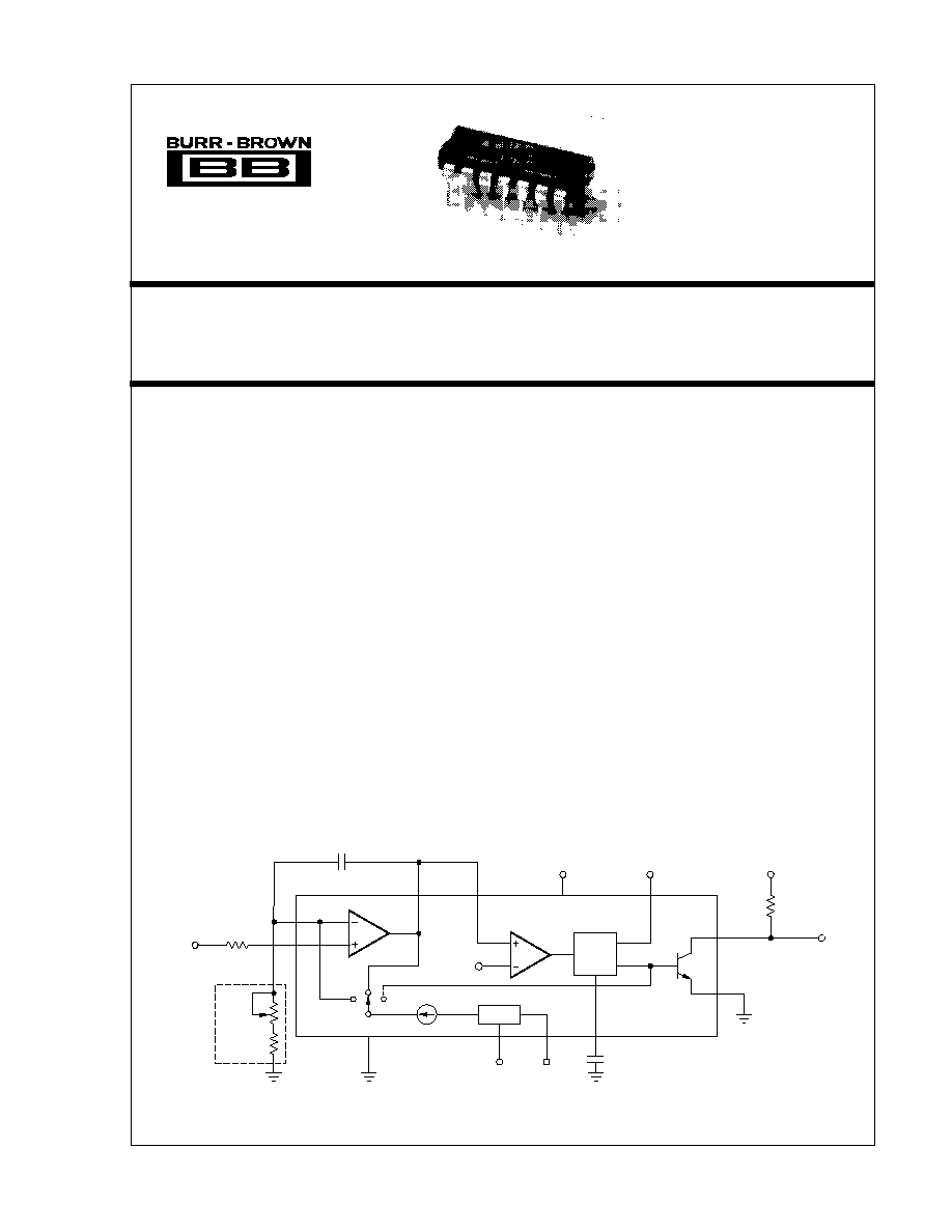
The VFC121 is a monolithic voltage-to-frequency
converter consisting of an integrating amplifier, volt-
age reference, and one-shot charge pump circuitry.
High-frequency complementary NPN/PNP circuitry is
used to implement the charge-balance technique,
achieving speed and accuracy far superior to previous
single power supply VFCs.
The high-impedance input accepts signals from ground
potential to V
S
≠ 2.5V. Power supplies from 4.5V to
36V may be used. A 2.6V reference voltage output
may be used to excite sensors or bias external cir-
cuitry. A thermometer output voltage proportional to
absolute temperature (
∞
K) may be used as a tempera-
ture sensor or for temperature compensation of appli-
cations circuits.
Frequency output is an open-collector transistor. A
disable pin forces the output to the high impedance
state, allowing multiple VFCs to share a common
transmission path.
2.6V
V
T
One
Shot
V
REF
V
REF
Comparator
Integrator
I
REF
12
11
10
9
13
2
14
8
6
3
5
4
R
TRIM
+V
S
+5V
Ground
(Optional)
R
PULL UP
V
PULL UP
C
INT
= 2700pF
V
IN
= 0 to +2V
R
BIAS
= 8k
(Optional)
R
IN
R
IN
= 8k
C
OS
= 1200pF
f
OUT
=
0 to 100kHz
© 1989 Burr-Brown Corporation
PDS-971A
Printed in U.S.A. March, 1992

Æ
VFC121
2
SPECIFICATIONS
ELECTRICAL
At T
A
= +25
∞
C, V
S
= +5V, and R
IN
= 8k
, unless otherwise noted.
VFC121AP
VFC121BP
PARAMETER
CONDITIONS
MIN
TYP
MAX
MIN
TYP
MAX
UNITS
ACCURACY
Nonlinearity: f
FS
= 100kHz
C
OS
1200pF, C
INT
= 2700pF
0.05
0.03
%FS
f
FS
= 1MHz
C
OS
68pF, C
INT
= 270pF
0.1
0.1
%FS
Gain Error:
f
FS
= 100kHz
C
OS
1200pF, C
INT
= 2700pF
10
*
%FS
Gain Drift:
f
FS
= 100kHz
T
MIN
to T
MAX
80
40
ppm/
∞
C
Relative to V
REF
+V
S
= +5V to +36V
100
40
ppm/
∞
C
PSRR
0.025
*
%/V
INPUT
Minimum Input Voltage
0
*
V
Maximum Input Voltage
V
S
≠ 2.5
V
S
≠ 2
*
*
V
Impedance
10
100
*
*
M
I
BIAS
150
300
*
*
nA
V
OS
300
800
100
400
µ
V
V
OS
Drift
T
MIN
to T
MAX
10
*
µ
V/
∞
C
OPEN COLLECTOR OUTPUT
V
SAT
I
PULL UP
= 10mA
0.4
*
V
I
LEAKAGE
V
PULL UP
= 5V
1
*
µ
A
V
PULL UP
= 36V
10
*
µ
A
Fall Time
100
*
ns
Delay to Rise
R
PULL UP
= 470
100
*
ns
Settling Time
To Specified Linearity for
(1)
Full Scale Input Step
REFERENCE VOLTAGE
Voltage
2.59
2.6
2.61
*
*
*
V
Voltage Drift
100
50
ppm/
∞
C
Load Regulation
I
O
= 0 to 10mA
10
*
mV
PSRR
V
S
= +5V to +36V
10
*
mV
Current Limit
Short Circuit Protected
INTEGRATOR AMPLIFIER OUTPUT
Output Voltage Range
R
L
= 100k
0.8
2.9
*
*
V
COMPARATOR INPUT
I
BIAS
+1
*
µ
A
Trigger Voltage
2.6
*
V
Input Voltage Range
0
2.9
*
*
V
THERMOMETER
V
T
T
A
= +25
∞
C
298
*
mV
V
T
Slope
T
MIN
to T
MAX
1
*
mV/
∞
K
DISABLE INPUT
V
HIGH
(Disabled)
2
*
V
V
LOW
0.8
*
V
I
HIGH
(Disabled)
V
HIGH
= 2V
10
*
µ
A
I
LOW
V
LOW
= 0.8V
10
*
µ
A
POWER SUPPLY
Voltage
4.5
5
36
*
*
*
V
Current
7.5
10
*
*
mA
TEMPERATURE RANGE
Specified
≠25
+85
*
*
∞
C
Storage
≠40
+125
*
*
∞
C
* Same specification as VFC121AP.
NOTE: (1) One pulse of new frequency plus 1
µ
s.
The information provided herein is believed to be reliable; however, BURR-BROWN assumes no responsibility for inaccuracies or omissions. BURR-BROWN assumes
no responsibility for the use of this information, and all use of such information shall be entirely at the user's own risk. Prices and specifications are subject to change
without notice. No patent rights or licenses to any of the circuits described herein are implied or granted to any third party. BURR-BROWN does not authorize or warrant
any BURR-BROWN product for use in life support devices and/or systems.
ORDERING INFORMATION
LINEARITY
ERROR, MAX
TEMPERATURE
MODEL
PACKAGE
(f
S
= 100kHz)
RANGE
1≠24
25≠99
100+
VFC121AP
Plastic DIP
0.05%
≠25
∞
C to +85
∞
C
VFC121BP
Plastic DIP
0.03%
≠25
∞
C to +85
∞
C
Æ
VFC121
3
PIN CONFIGURATION
PIN CONFIGURATION
PIN #
NAME
DESCRIPTION
1
NC
Not Connected
2
Disable
Input logic Low for normal operation. Input logic
High to disable the VFC121. Has internal pull-
down, for normal operation if not connected.
3
V
T
Temperature compensation voltage proportional
to absolute temperature. Typically 298mV at
room temperature (298
∞
K), with a change of
1mV per
∞
C (
∞
K).
4
Gnd Sense
Defines ground for the internal voltage reference.
5
C
OS
One-shot capacitor is connected between here
and ground to set full scale output frequency.
6
V
REF
Output from the internal band-gap voltage
reference, typically 2.6V. Can be used
externally to set levels or excite sensors.
7
NC
Not Connected
8
Gnd
Ground
9
Comp In
Comparator In
10
Int Out
Integrator Out
11
+V
IN
Non-inverting input of the integrating op amp.
The input signal is applied here.
12
≠V
IN
Inverting input of the integrating op amp. C
INT
is
connected between here and the integrator
output (pin 10), and R
IN
is connected between
here and ground.
13
+V
S
Supply voltage connected here. Range is +4.5V
to +36V.
14
f
OUT
Frequency output pin. This is the output of an
open-collector transistor, and an external pull-
up circuit should be used to generate the appro-
priate logic levels.
ABSOLUTE MAXIMUM RATINGS
Power Supply Voltage (+V
S
) ................................................................ 40V
f
OUT
Sink Current ............................................................................... 20mA
Comparator In Voltage .......................................................... ≠0.5V to +3V
Enable Input ........................................................................... ≠0.3V to +V
S
Integrator Common-Mode Voltage ..................................... 0V to +V
S
≠ 2V
Integrator Differential Input Voltage ................................... ≠0.3V to +0.3V
V
REF
Out (short-circuit) ................................................................. Indefinite
Operating Temperature Range ......................................... ≠40
∞
C to +85
∞
C
Storage Temperature ...................................................... ≠40
∞
C to +125
∞
C
Lead Temperature (soldering, 10s) ................................................ +300
∞
C
Stresses above these ratings may permanently damage the device. Expo-
sure to absolute maximum rating conditions for extended periods may affect
device reliability.
Top View
PACKAGE INFORMATION
PACKAGE DRAWING
MODEL
PACKAGE
NUMBER
(1)
VFC121AP
14-Pin Plastic DIP
010
VFC121BP
14-Pin Plastic DIP
010
NOTE: (1) For detailed drawing and dimension table, please see end of data
sheet, or Appendix D of Burr-Brown IC Data Book.
f
+V
≠V
+V
Int Out
Comp In
Gnd
NC
Disable
Gnd Sense
NC
T
1
2
3
4
5
6
7
14
13
12
11
10
9
8
OS
REF
V
C
V
IN
IN
S
OUT
Æ
VFC121
4
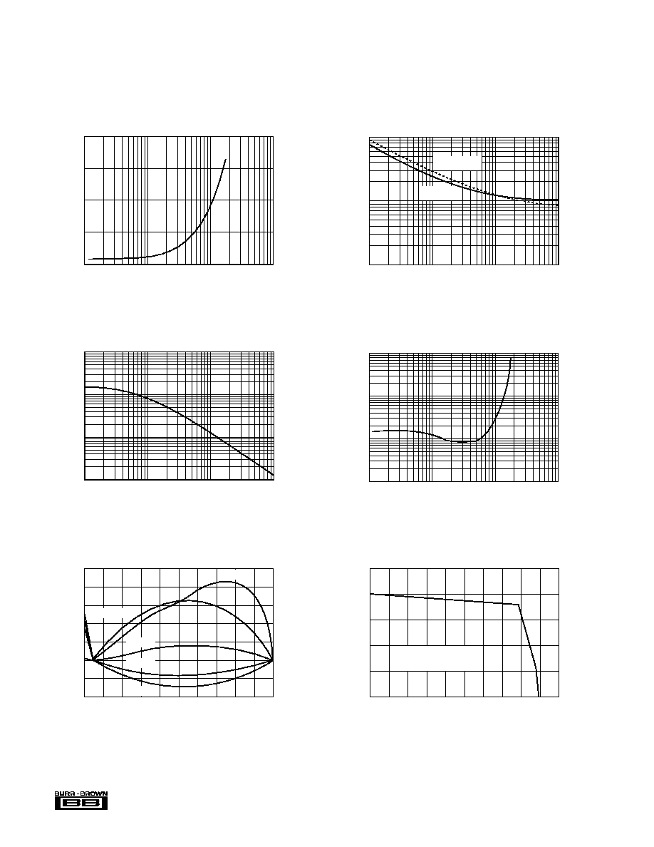
REFERENCE VOLTAGE
vs REFERENCE LOAD CURRENT
2.62
2.6
2.58
2.56
2.54
2.52
0
2
4
6
8
10
12
14
16
18
20
Output Current (mA)
V (V)
REF
NOTE: The V output is
short-circuit protected.
REF
NON-LINEARITY vs INPUT VOLTAGE
0
0.2
0.4
0.6
0.8
1
1.2
1.4
1.6
1.8
2
Input Voltage (V)
Linearity Error (% of FSR)
0.04
0.02
0
≠0.02
0.2
0.1
0
≠0.1
1.5MHz
1MHz
500kHz
250kHz
10kHz
Linearity Error (% of FSR) for
1.5MHz Full Scale Frequency
NON-LINEARITY
vs FULL-SCALE FREQUENCY
1
0.1
0.01
0.001
10
4
10
5
10
6
10
7
Full-Scale Frequency (Hz)
Non-Linearity (% of FSR)
FULL SCALE FREQUENCY
vs EXTERNAL ONE-SHOT CAPACITOR
10
7
10
6
10
5
4
10
10
100
1000
10000
External One-Shot Capacitor (pF)
Full Scale Frequency (Hz)
700
600
500
400
300
JITTER vs FULL SCALE FREQUENCY
10
10
10
10
4
5
6
7
Full Scale Frequency (Hz)
Jitter (ppm)
TYPICAL PERFORMANCE CURVES
At T
A
= +25
∞
C, V
S
= +5V, and R
IN
= 8k
, unless otherwise noted.
0.001%
0.0001%
0.00001%
1
10
100
1000
FREQUENCY COUNT REPEATABILITY
vs COUNTER GATE TIME
Time (ms)
Frequency Repeatability (%)
f = 100kHz
FS
f = 1MHz
FS
Æ
VFC121
5
FULL SCALE GAIN DRIFT vs TEMPERATURE
≠25
Ambient Temperature (∞C)
Change (%)
0
25
50
75
100
f = 1.5MHz
FS
f =
FS
f =
FS
f =
FS
f =
FS
f =
FS
1MHz
500kHz
200kHz
100kHz
10kHz
6
5
4
3
2
1
0
QUIESCENT CURRENT vs TEMPERATURE
≠50
≠25
0
25
50
75
100
125
Ambient Temperature (∞C)
Quiescent Current (mA)
V = +36V
S
V = +12V
S
V = +5V
S
10
9.5
9
8.5
8
7.5
7
TYPICAL PERFORMANCE CURVES
(CONT)
At T
A
= +25
∞
C, V
S
= +5V, and R
IN
= 8k
, unless otherwise noted.
THEORY OF OPERATION
The VFC121 uses a charge-balance technique to achieve
high accuracy. The basic architecture is shown in Figure 1.
An analog integrator at the front end, consisting of a preci-
sion op amp and a feedback capacitor, C
INT
, provides a true
integrating approach for improved noise immunity. Use of
the non-inverting input of the op amp for the analog input
provides a high input impedance to the user.
The integrator's output is proportional to the charge stored
on C
INT
plus the analog input voltage. An input voltage, V
IN
,
forces a current through R
IN
of V
IN
/R
IN
, which also flows
through C
INT
. This current through C
INT
causes the integra-
tor output to ramp positive. (Refer to the timing diagram in
Figure 2.)
When the output of the integrator ramps to V
REF
, the com-
parator trips, driving the output of the VFC121 Low, and
triggering the one-shot. The tripping of the comparator also
connects the reference current, I
REF
, to the integrator input
for the duration of the one-shot period, T
OS
. This switched
current causes the output of the integrator to ramp negative.
When the one-shot times out, the output of the VFC121 is
reset High, the one-shot is reset, and I
REF
is switched to the
output of the integrating op amp. (This causes the output of
FIGURE 2. Timing Diagram.
FIGURE 1. VFC121 Architecture.
V
IN
V
REF
V
T
One
Shot
V
REF
V
REF
C
OS
Comparator
Integrator
I
REF
12
11
10
9
13
2
14
8
6
3
5
4
R
IN
f
OUT
+V
S
C
INT
V (2.6V)
REF
Effect of
a smaller
C
INT
Integrator
Output
(pin 10)
f
(pin 14)
OUT
1/ f
OUT