 | ÐлекÑÑоннÑй компоненÑ: XTR101 | СкаÑаÑÑ:  PDF PDF  ZIP ZIP |
Äîêóìåíòàöèÿ è îïèñàíèÿ www.docs.chipfind.ru
©
1986 Burr-Brown Corporation
PDS-627G
Printed in U.S.A. October, 1993
International Airport Industrial Park · Mailing Address: PO Box 11400, Tucson, AZ 85734 · Street Address: 6730 S. Tucson Blvd., Tucson, AZ 85706 · Tel: (520) 746-1111 · Twx: 910-952-1111
Internet: http://www.burr-brown.com/ · FAXLine: (800) 548-6133 (US/Canada Only) · Cable: BBRCORP · Telex: 066-6491 · FAX: (520) 889-1510 · Immediate Product Info: (800) 548-6132
XTR101
Precision, Low Drift
4-20mA TWO-WIRE TRANSMITTER
FEATURES
q
INSTRUMENTATION AMPLIFIER INPUT
Low Offset Voltage, 30
µ
V max
Low Voltage Drift, 0.75
µ
V/
°
C max
Low Nonlinearity, 0.01% max
q
TRUE TWO-WIRE OPERATION
Power and Signal on One Wire Pair
Current Mode Signal Transmission
High Noise Immunity
q
DUAL MATCHED CURRENT SOURCES
q
WIDE SUPPLY RANGE: 11.6V to 40V
q
40
°
C to +85
°
C SPECIFICATION RANGE
q
SMALL 14-PIN DIP PACKAGE, CERAMIC
AND PLASTIC
APPLICATIONS
q
INDUSTRIAL PROCESS CONTROL
Pressure Transmitters
Temperature Transmitters
Millivolt Transmitters
q
RESISTANCE BRIDGE INPUTS
q
THERMOCOUPLE INPUTS
q
RTD INPUTS
q
CURRENT SHUNT (mV) INPUTS
q
PRECISION DUAL CURRENT SOURCES
q
AUTOMATED MANUFACTURING
q
POWER/PLANT ENERGY SYSTEM
MONITORING
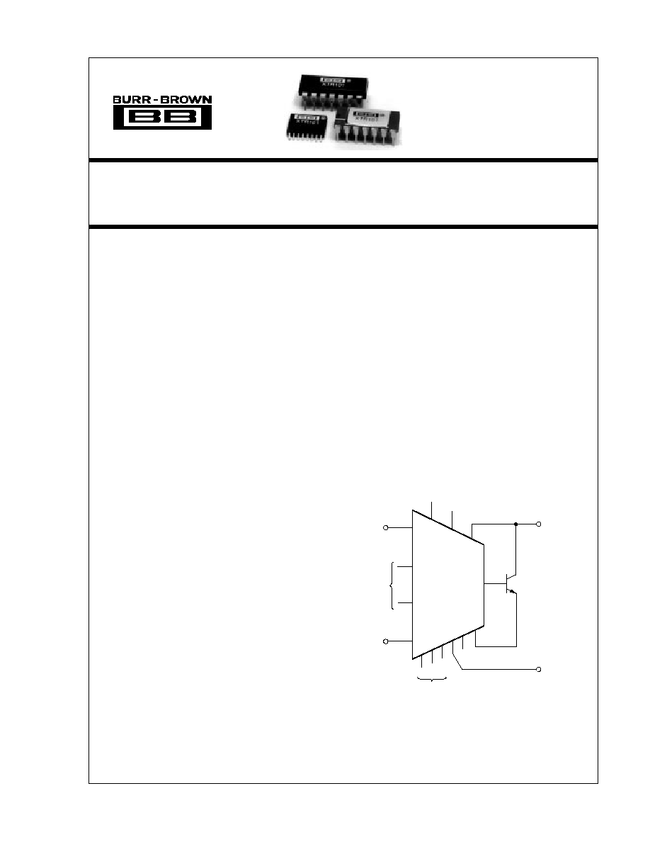
DESCRIPTION
The XTR101 is a microcircuit, 4-20mA, two-wire
transmitter containing a high accuracy instrumenta-
tion amplifier (IA), a voltage-controlled output current
source, and dual-matched precision current reference.
This combination is ideally suited for remote signal
conditioning of a wide variety of transducers such as
thermocouples, RTDs, thermistors, and strain gauge
bridges. State-of-the-art design and laser-trimming,
wide temperature range operation and small size make
it very suitable for industrial process control applica-
tions. In addition, the optional external transistor al-
lows even higher precision.
The two-wire transmitter allows signal and power to
be supplied on a single wire-pair by modulating the
power supply current with the input signal source. The
transmitter is immune to voltage drops from long runs
and noise from motors, relays, actuators, switches,
transformers, and industrial equipment. It can be used
by OEMs producing transmitter modules or by data
acquisition system manufacturers.
2
B
14
9
1
8
11
10
3
5
6
4
XTR101
e
1
12
Optional
Offset Null
Optional
External
Transistor
REF1
I
REF2
I
I
OUT
7
13
E
(1)
(1)
e
2
Span
NOTE: (1) Pins 12 and 13 are used for optional BW control.
+
+V
CC
®

®
XTR101
2
SPECIFICATIONS
ELECTRICAL
At T
A
= +25
°
C, +V
CC
= 24VDC, and R
L
= 100
with external transistor connected, unless otherwise noted
T
Same as XTR101AG.
NOTES: (1) See Typical Performance Curves. (2) Span error shown is untrimmed and may be adjusted to zero. (3) e
1
and e
2
are signals on the In and +In terminals
with respect to the output, pin 7. While the maximum permissible
e is 1V, it is primarily intended for much lower input signal levels, e.g., 10mV or 50mV full scale
for the XTR101A and XTR101B grades respectively. 2mV FS is also possible with the B grade, but accuracy will degrade due to possible errors in the low value
span resistance and very high amplification of offset, drift, and noise. (4) Offset voltage is trimmed with the application of a 5V common-mode voltage. Thus the
associated common-mode error is removed. See Application Information section.
The information provided herein is believed to be reliable; however, BURR-BROWN assumes no responsibility for inaccuracies or omissions. BURR-BROWN assumes
no responsibility for the use of this information, and all use of such information shall be entirely at the user's own risk. Prices and specifications are subject to change
without notice. No patent rights or licenses to any of the circuits described herein are implied or granted to any third party. BURR-BROWN does not authorize or warrant
any BURR-BROWN product for use in life support devices and/or systems.
XTR101AG
XTR101BG
XTR101AP
XTR101AU
PARAMETER
CONDITIONS
MIN
TYP
MAX
MIN
TYP
MAX
MIN
TYP
MAX
MIN
TYP
MAX
UNITS
OUTPUT AND LOAD CHARACTERISTICS
Current
Linear Operating Region
4
20
T
T
T
T
T
T
mA
Derated Performance
3.8
22
T
T
T
T
T
T
mA
Current Limit
28
38
T
T
31
T
31
T
mA
Offset Current Error
I
OS
, I
O
= 4mA
±
3.9
±
10
±
2.5
±
6
±
8.5
±
19
±
8.5
±
19
µ
A
vs Temperature
I
OS
/
T
±
10.5
±
20
±
8
±
15
±
10.5
±
20
T
ppm, FS/
°
C
Full Scale Output Current Error
Full Scale = 20mA
±
20
±
40
±
15
±
30
±
30
±
60
±
30
±
60
µ
A
Power Supply Voltage
V
CC
, Pins 7 and 8,
+11.6
±
40
T
T
T
T
T
T
VDC
Compliance
(1)
Load Resistance
At V
CC
= +24V, I
O
= 20mA
600
T
600
T
At V
CC
= +40V, I
O
= 20mA
1400
T
1400
T
SPAN
Output Current Equation
R
S
in
, e
1
and e
2
in V
i
O
= 4mA + [0.016
+ (40/R
S
)] (e
2
e
1
)
Span Equation
R
S
in
S = [0.016
+ (40/R
S
)]
A/V
vs Temperature
Excluding TCR of R
S
±
30
±
100
T
T
T
T
T
T
ppm/
°
C
Untrimmed Error
(2)
SPAN
5
2.5
0
T
T
T
T
T
T
T
T
T
%
Nonlinearity
NONLINEARITY
0.01
T
T
T
%
Hysteresis
0
T
T
T
%
Dead Band
0
T
T
T
%
INPUT CHARACTERISTICS
Impedance: Differential
0.4 || 3
T
T
T
G
|| pF
Common -Mode
10 || 3
T
T
T
G
|| pF
Voltage Range, Full Scale
e = (e
2
e
1
)
(3)
0
1
T
T
T
T
T
T
V
Offset Voltage
V
OS
±
30
±
60
±
20
±
30
T
±
100
T
±
100
µ
V
vs Temperature
V
OS
/
T
±
0.75
±
1.5
±
0.35
±
0.75
T
T
T
T
µ
V/
°
C
Power Supply Rejection
V
CC
/PSRR = V
OS
Error
110
125
T
T
T
122
110
122
dB
Bias Current
I
B
60
150
T
T
T
T
T
T
nA
vs Temperature
I
B
/
T
0.30
1
T
T
T
T
T
T
nA/
°
C
Offset Current
I
OSI
10
±
30
T
±
20
T
T
T
T
nA
vs Temperature
I
OSI
/
T
0.1
0.3
T
T
T
T
T
T
nA/
°
C
Common-Mode Rejection
(4)
DC
90
100
T
T
T
T
T
T
dB
Common-Mode Range
e
1
and e
2
with Respect
to Pin 7
4
6
T
T
T
T
T
T
V
CURRENT SOURCES
Magnitude
1
T
T
T
mA
Accuracy
V
CC
= 24V,
V
PIN 8
V
PIN 10
,
11
= 19V
R
2
= 5k
, Fig. 5
±
0.06
±
0.17
±
0.025
±
0.075
±
0.2
±
0.37
±
0.2
±
0.37
%
vs Temperature
±
50
±
80
±
30
±
50
T
T
T
T
ppm/
°
C
vs V
CC
±
3
T
T
T
ppm/V
vs Time
±
8
T
T
T
ppm/month
Compliance Voltage
With Respect to Pin 7
0
V
CC
3.5
T
T
T
T
T
T
V
Ratio Match
Tracking
Accuracy
(1 I
REF1
/I
REF2
)
X
100%
±
0.014
±
0.06
±
0.009
±
0.04
±
0.031
±
0.088
±
0.031
±
0.088
%
vs Tempeature
±
15
10
T
T
ppm/
°
C
vs V
CC
±
10
T
T
T
ppm/V
vs Time
±
1
T
T
T
ppm/month
Output Impedance
10
20
T
T
T
15
T
15
M
TEMPERATURE RANGE
Specification
40
+85
T
T
40
+85
T
T
°
C
Operating
55
+125
T
T
40
+85
40
+85
°
C
Storage
55
+165
T
T
55
+125
55
+125
°
C
®
XTR101
3
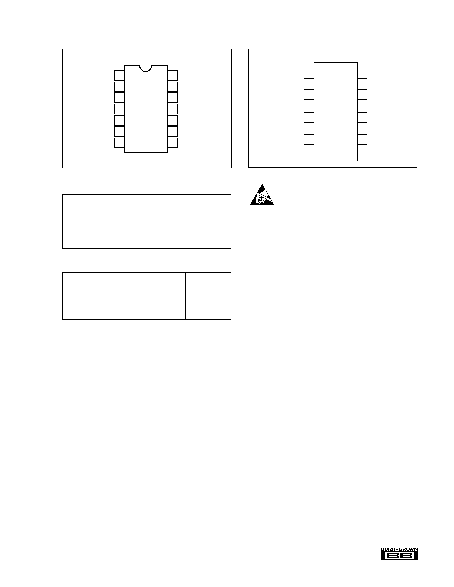
PIN CONFIGURATION
Top View
DIP
Top View
SOIC
Zero Adjust
Zero Adjust
In
+In
Span
Span
Out
NC
Zero Adjust
Bandwidth
B Control
I
REF2
I
REF1
E
+V
CC
NC
1
2
3
4
5
6
7
8
16
15
14
13
12
11
10
9
SOL-16
Surface-Mount
Zero Adjust
Zero Adjust
In
+In
Span
Span
Out
Zero Adjust
Bandwidth
B Control
I
REF2
I
REF1
E
+V
CC
1
2
3
4
5
6
7
14
13
12
11
10
9
8
DIP
PACKAGE
DRAWING
TEMPERATURE
PRODUCT
PACKAGE
NUMBER
(1)
RANGE
XTR101AG
14-Pin Ceramic DIP
169
40
°
C to +85
°
C
XTR101BG
14-Pin Ceramic DIP
169
40
°
C to +85
°
C
XTR101AP
14-Pin Plastic DIP
010
40
°
C to +85
°
C
XTR101AU
16-Lead SOIC
211
40
°
C to +85
°
C
NOTE: (1) For detailed drawing and dimension table, please see end of data
sheet, or Appendix C of Burr-Brown IC Data Book.
ABSOLUTE MAXIMUM RATINGS
Power Supply, +V
CC
........................................................................... 40V
Input Voltage, e
1
or e
2
........................................................
V
OUT
,
+V
CC
Storage Temperature Range, Ceramic ........................ 55
°
C to +165
°
C
Plastic ............. 55
°
C to +125
°
C
Lead Temperature (soldering 10s) G, P ...................................... +300
°
C
(wave soldering, 3s) U .......................... +260
°
C
Output Short-Circuit Duration ........................... Continuous +V
CC
to I
OUT
Junction Temperature ................................................................... +165
°
C
PACKAGE/ORDERING INFORMATION
ELECTROSTATIC
DISCHARGE SENSITIVITY
This integrated circuit can be damaged by ESD. Burr-Brown
recommends that all integrated circuits be handled with
appropriate precautions. Failure to observe proper handling
and installation procedures can cause damage.
ESD damage can range from subtle performance degrada-
tion to complete device failure. Precision integrated circuits
may be more susceptible to damage because very small
parametric changes could cause the device not to meet its
published specifications.
®
XTR101
4
TYPICAL PERFORMANCE CURVES
At T
A
= +25
°
C, +V
CC
= 24VDC, unless otherwise noted.
100
1k
10k
100k
0
Frequency (Hz)
SPAN vs FREQUENCY
1M
80
60
40
20
Transconductance (20 Log m
)
R
S
= 25
R
S
= 100
R
S
= 400
R
S
= 2k
R
S
=
C
C
= 0
0
Time (µs)
STEP RESPONSE
25
20
15
10
5
Output Current (mA)
0
200
400
600
800
1000
R
S
= 25
R
S
=
0
100
200
300
0
R
S
(
)
FULL SCALE INPUT VOLTAGE vs R
S
400
0.08
0.06
0.04
0.02
e
IN
Full Scale (V)
0 to 800mV and
0 to 8k
scale
0
0.8
0.6
0.4
0.2
e
IN
Full Scale (V)
0
2
4
6
8
R
S
(k
)
0 to 80mV (low level signals)
and 0 to 400
scale
0
0.1
1
10
100
1k
10k
Frequency (Hz)
CMR (dB)
COMMON-MODE REJECTION vs FREQUENCY
100k
120
100
80
60
40
20
120
100
80
60
40
20
0.1
0
Frequency (Hz)
Power Supply Rejection (dB)
POWER SUPPLY REJECTION vs FREQUENCY
140
10
100
1k
100k
1M
10M
10k
0.1
1
10
100
1k
10k
100k
Bandwidth Control, C
C
(pF)
Bandwidth (Hz)
BANDWIDTH vs PHASE COMPENSATION
1M
100k
10k
1k
100
10
1
R
S
= 25
R
S
= 100
R
S
= 400
R
S
=
®
XTR101
5
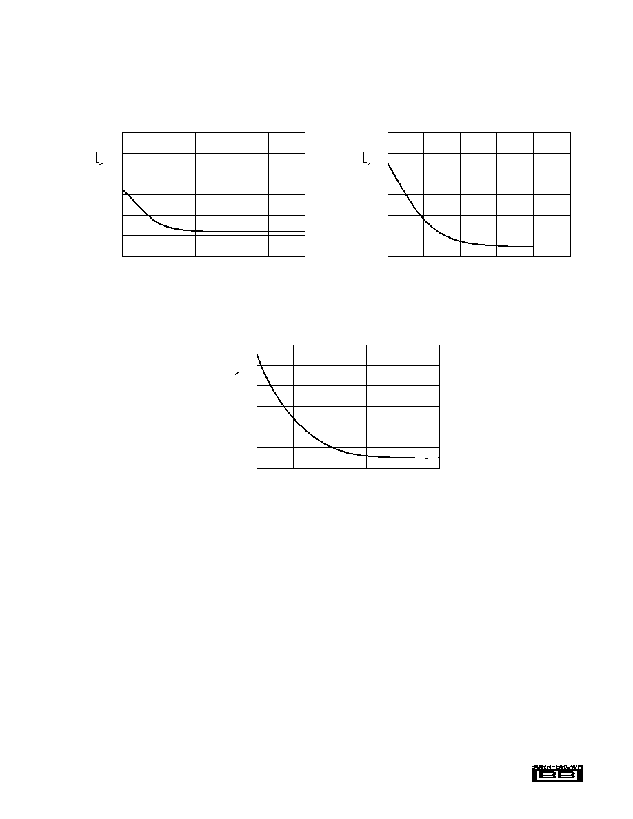
TYPICAL PERFORMANCE CURVES
(CONT)
At T
A
= +25
°
C, +V
CC
= 24VDC, unless otherwise noted.
10
1
10
100
1k
10k
0
Frequency (Hz)
INPUT VOLTAGE NOISE DENSITY vs FREQUENCY
100k
60
50
40
30
20
Input Noise Voltage (nV/ Hz
)
0
Frequency (Hz)
INPUT CURRENT NOISE DENSITY vs FREQUENCY
6
5
4
3
2
1
Input Noise Current (pA/ Hz
)
1
10
100
1k
10k
100k
0
Frequency (Hz)
OUTPUT CURRENT NOISE DENSITY vs FREQUENCY
6
5
4
3
2
1
Output Noise Current (nA/ Hz
)
1
10
100
1k
10k
100k
THEORY OF OPERATION
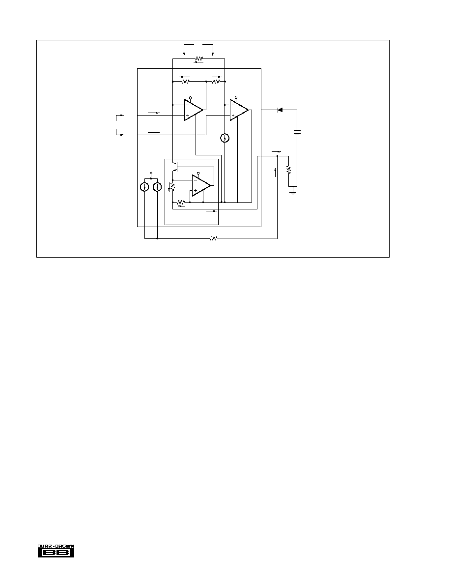
A simplified schematic of the XTR101 is shown in Figure 1.
Basically the amplifiers, A
1
and A
2
, act as a single power
supply instrumentation amplifier controlling a current source,
A
3
and Q
1
. Operation is determined by an internal feedback
loop. e
1
applied to pin 3 will also appear at pin 5 and
similarly e
2
will appear at pin 6. Therefore the current in R
S
,
the span setting resistor, will be I
S
= (e
2
e
1
)/R
S
= e
IN
/R
S
.
This current combines with the current, I
3
, to form I
1
. The
circuit is configured such that I
2
is 19 times I
1
. From this
point the derivation of the transfer function is straightfor-
ward but lengthy. The result is shown in Figure 1.
Examination of the transfer function shows that I
O
has a
lower range-limit of 4mA when e
IN
= e
2
e
1
= 0V. This 4mA
is composed of 2mA quiescent current exiting pin 7 plus
2mA from the current sources. The upper range limit of I
O
is
set to 20mA by the proper selection of R
S
based on the upper
range limit of e
IN
. Specifically R
S
is chosen for a 16mA
output current span for the given full scale input voltage
span; i.e., (0.016
+ 40/R
S
)(e
IN
full scale) = 16mA. Note that
since I
O
is unipolar e
2
must be kept larger than e
1
; i.e., e
2
e
1
or e
IN
0. Also note that in order not to exceed the output
upper range limit of 20mA, e
IN
must be kept less than 1V
when R
S
=
and proportionately less as R
S
is reduced.
INSTALLATION AND
OPERATING INSTRUCTIONS
BASIC CONNECTION
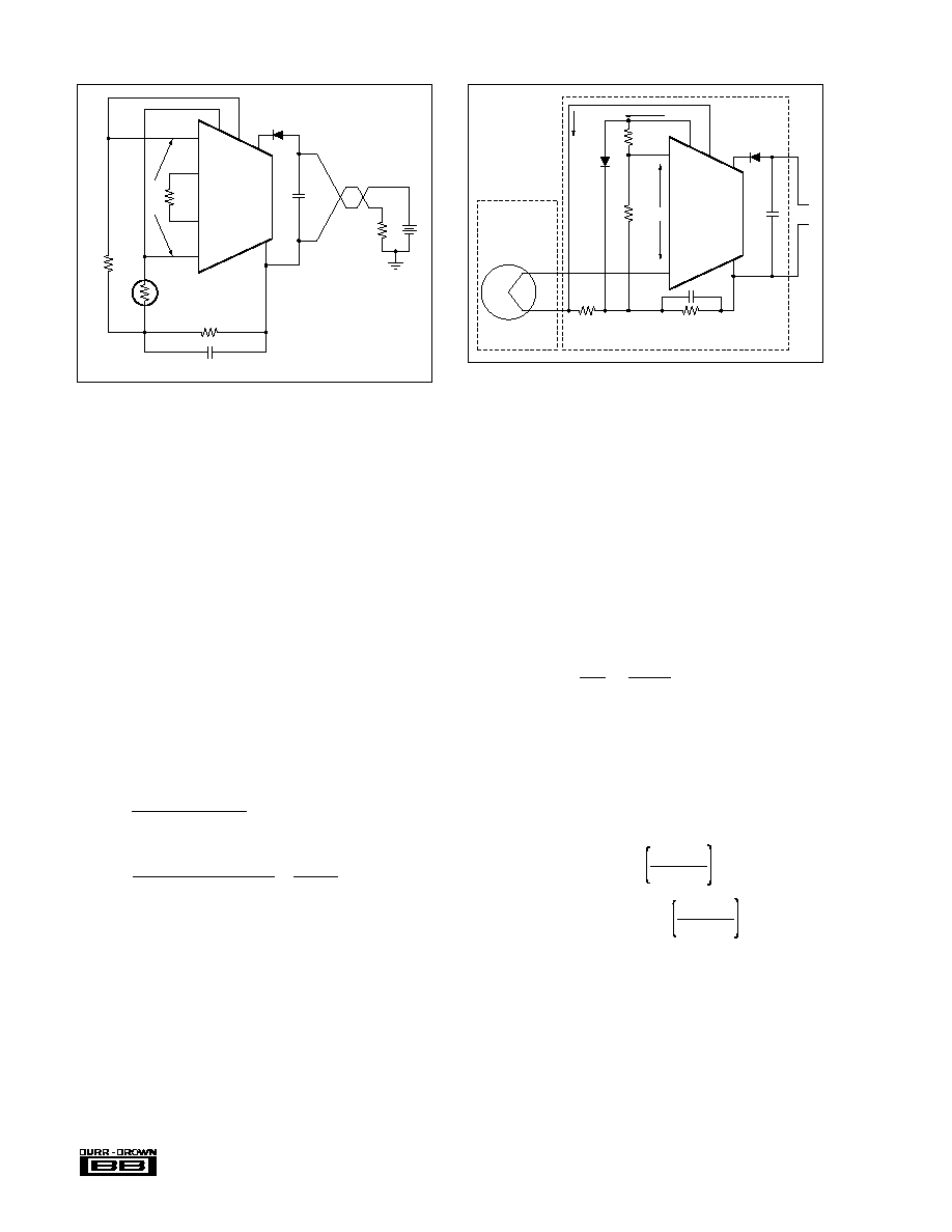
The basic connection of the XTR101 is shown in Figure 1.
A difference voltage applied between input pins 3 and 4 will
cause a current of 4-20mA to circulate in the two-wire
output loop (through R
L
, V
PS
, and D
1
). For applications
requiring moderate accuracy, the XTR101 operates very
cost-effectively with just its internal drive transistor. For
more demanding applications (high accuracy in high gain)
an external NPN transistor can be added in parallel with the
internal one. This keeps the heat out of the XTR101 package
®
XTR101
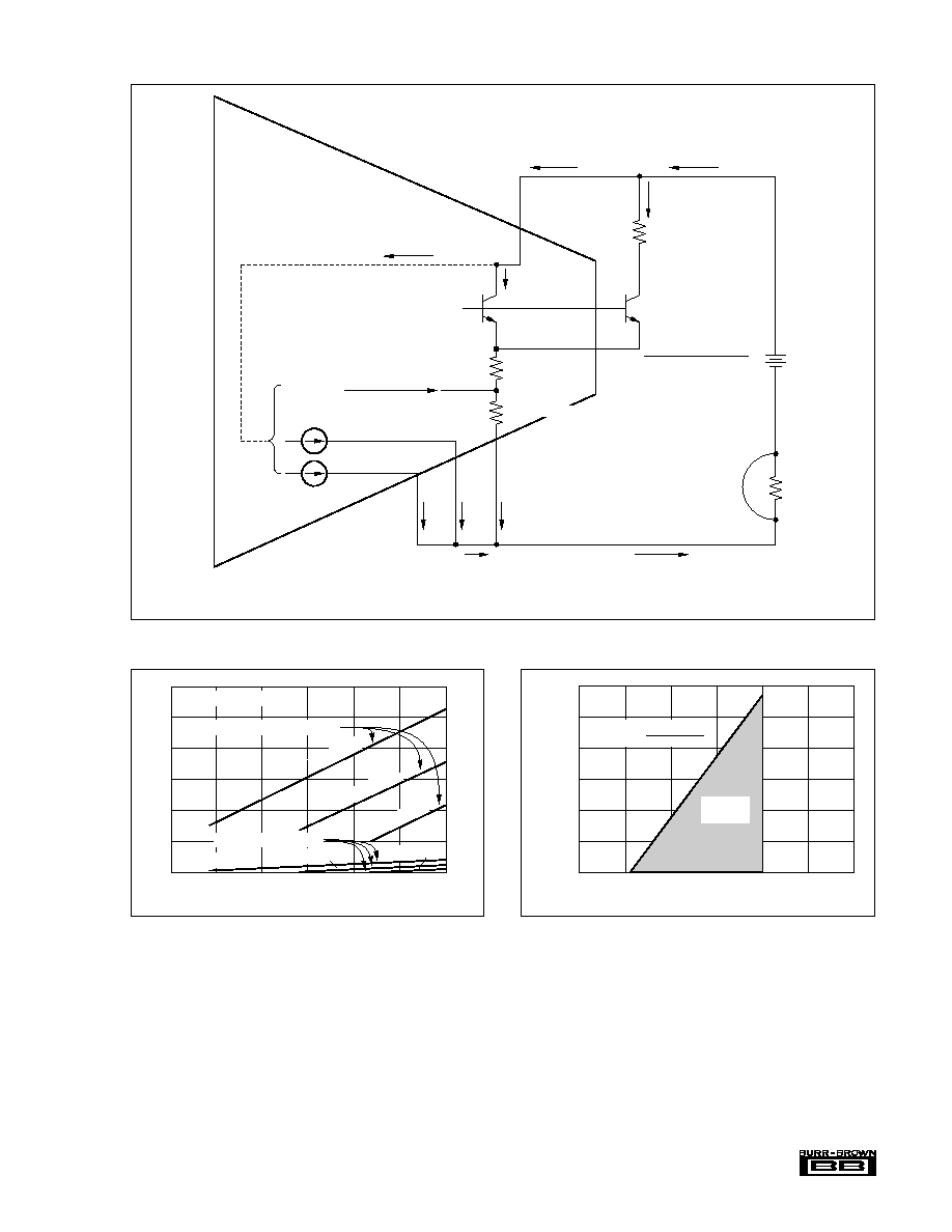
6
+V
CC
A
1
+V
CC
D
1
V
PS
I
O
7
e
L
10
11
Q
1
R1
Voltage Controlled
Current Source
2.5k
100µA
1.25k
8
5
6
2mA
R2
52.6
(e
2
)
I
B1
I
B2
I
2
I
REF1
1k
e
IN
I
S
(e
2
)
(e
1
)
I
3
I
4
R
3
+
I
1
+
A
3
I
O
= 4mA + (0.016 + 40/R
S
) e
IN
, e
IN
= e
2
e
1
(e
1
)
R
S
In
3
+In
4
e
IN
I
REF2
I
O
+V
CC
1.25k
R
4
+V
CC
+V
CC
R
L
A
2
FIGURE 1. Simplified Schematic of the XTR101.
and minimizes thermal feedback to the input stage. Also in
such applications where e
IN
full scale is small (<50mV) and
R
SPAN
is small (<150
), caution should be taken to consider
errors from the external span circuit plus high amplification
of offset drift and noise.
OPTIONAL EXTERNAL TRANSISTOR
The optional external transistor, when used, is connected in
parallel with the XTR101's internal transistor. The purpose
is to increase accuracy by reducing heat change inside the
XTR101 package as the output current spans from 4-20mA.
Under normal operating conditions, the internal transistor is
never completely turned off as shown in Figure 2. This
maintains frequency stability with varying external transis-
tor characteristics and wiring capacitance. The actual "cur-
rent sharing" between internal and external transistors is
dependent on two factors: (1) relative geometry of emitter
areas and (2) relative package dissipation (case size and
thermal conductivity). For best results, the external device
should have a larger base-emitter area and smaller package.
It will, upon turn on, take about [0.95 (I
O
3.3mA)]mA.
However, it will heat faster and take a greater share after a
few seconds.
Although any NPN of suitable power rating will operate
with the XTR101, two readily available transistors are
recommended.
1. 2N2222 in the TO-18 package. For power supply volt-
ages above 24V, a 750
, 1/2W resistor should be con-
nected in series with the collector. This will limit the
power dissipation to 377mW under the worst-case condi-
tions shown in Figure 2. Thus the 2N2222 will safely
operate below its 400mW rating at the upper temperature
of +85
°
C. Heat sinking the 2N2222 will result in greatly
reduced accuracy improvement and is not recommended.
2. TIP29B in the TO-220 package. This transistor will
operate over the specified temperature and output voltage
range without a series collector resistor. Heat sinking the
TIP29B will result in slightly less accuracy improvement.
It can be done, however, when mechanical constraints
require it.
ACCURACY WITH AND
WITHOUT EXTERNAL TRANSISTOR
The XTR101 has been tested in a circuit using an external
transistor. The relative difference in accuracy with and
without an external transistor is shown in Figure 3. Notice
that a dramatic improvement in offset voltage change with
supply voltage is evident for any value of load resistor.
MAJOR POINTS TO
CONSIDER WHEN USING THE XTR101
1. The leads to R
S
should be kept as short as possible to
reduce noise pick-up and parasitic resistance.
2. +V
CC
should be bypassed with a 0.01
µ
F capacitor as close
to the unit as possible (pin 8 to 7).
3. Always keep the input voltages within their range of
linear operation, +4V to +6V (e
1
and e
2
measured with
respect to pin 7).
®
XTR101
7
1mA
10
7
1mA
11
Q
EXT
23.6V, 377mW
12
B
210
52.6
1.5mA
Quiescent
18mA
20mA
R
L
250
Short Circuit
Worst Case
V
PS
40V
20mA
4mA
16mA
750
12V, 200mW
Q
INT
18mW
+V
CC
8
I
OUT
NOTES: (1) An external transistor is used in the maufacturing test circuit for testing electrical specifications.
(2) This resistor is required for the 2N2222 with V
PS
> 24V to limit power dissipation.
3.47V, 60mW
XTR101
3.5mA
0.95V, 17mW
E
(2)
2N2222
(1)
2mA
9
0.5mA
Type
2N4922
TIP29B
TIP31B
Package
TO-225
TO-220
TO-220
Other Suitable Types
FIGURE 2. Power Calculation of XTR101 with External Transistor.
FIGURE 3. Thermal Feedback Due to Change in Output
Current.
FIGURE 4. Power Supply Operating Range.
4. The maximum input signal level (e
INFS
) is 1V with R
S
=
and proportionally less as R
S
decreases.
5. Always return the current references (pins 10 and 11) to
the output (pin 7) through an appropriate resistor. If the
references are not used for biasing or excitation, connect
them together to pin 7. Each reference must have between
0V and +(V
CC
4V) with respect to pin 7.
6. Always choose R
L
(including line resistance) so that the
voltage between pins 7 and 8 (+V
CC
) remains within the
11.6V to 40V range as the output changes between the
4-20mA range (see Figure 4).
7. It is recommended that a reverse polarity protection diode
(D
1
in Figure 1) be used. This will prevent damage to the
XTR101 caused by a momentary (e.g., transient) or long
term application of the wrong polarity of voltage between
pins 7 and 8.
V
CC
(V)
Self-Heating
Temperature (°C)
V
OS
(µV)
30
25
20
15
10
5
0
10
20
30
40
60
50
40
30
20
10
0
With external transistor
R
L
= 100
R
L
= 600
R
L
= 1k
R
L
= 100
R
L
= 600
R
L
= 1k
Without external transistor
Span =
I
O
= 16mA
1500
1250
1000
750
500
250
0
10
20
30
40
50
60
0
Power Supply Voltage, V
PS
(V)
Load Resistance, R
L
(
)
R
L
max =
V
PS
11.6V
20mA
Operating
Region
®
XTR101
8
8. Consider PC board layout which minimizes parasitic
capacitance, especially in high gain.
SELECTING R
S
R
SPAN
is chosen to that a given full scale input span e
INFS
will result in the desired full scale output span of
I
OFS
,
[(0.016 ) + (40/R
S
)]
e
IN
=
I
O
= 16mA.
Solving for R
S
:
R
S
=
For example, if
e
INFS
= 100mV for
I
OFS
= 16mA,
R
S
=
=
=
= 278
See Typical Performance Curves for a plot of R
S
vs
e
INFS
.
Note that in order not to exceed the 20mA upper range limit,
e
IN
must be less than 1V when R
S
=
and proportionately
smaller as R
S
decreases.
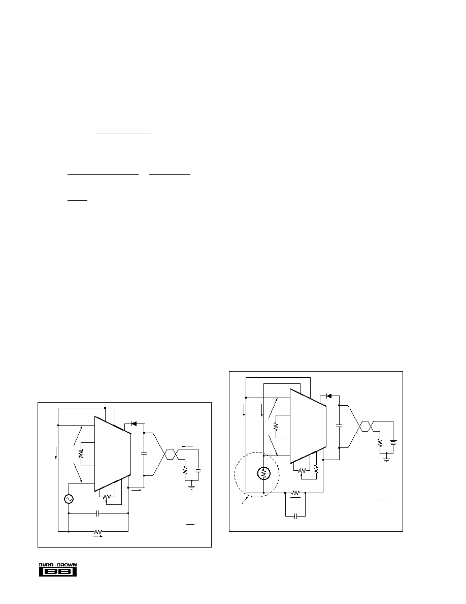
BIASING THE INPUTS
Because the XTR operates from a single supply both e
1
and
e
2
must be biased approximately 5V above the voltage at pin
7 to assure linear response. This is easily done by using one
or both current sources and an external resistor R
2
. Figure 5
shows the simplest case-- a floating voltage source e'
2
. The
2mA from the current sources flows through the 2.5k
value of R
2
and both e
1
and e
2
are raised by the required 5V
with respect to pin 7. For linear operation the constraint is
+4V
e
1
+6V
+4V
e
2
+6V
The offset adjustment is used to remove the offset voltage of
the input amplifier. When the input differential voltage (e
IN
)
equals zero, adjust for 4mA output.
Figure 6 shows a similar connection for a resistive trans-
ducer. The transducer could be excited either by one (as
shown) or both current sources. Also, the offset adjustment
has higher resolution compared to Figure 5.
CMV AND CMR
The XTR101 is designed to operate with a nominal 5V
common-mode voltage at the input and will function prop-
erly with either input operating over the range of 4V to 6V
with respect to pin 7. The error caused by the 5V CMV is
already included in the accuracy specifications.
If the inputs are biased at some other CMV then an input
offset error term is (CMV 5)/CMRR; CMR is in dB,
CMRR is in V/V.
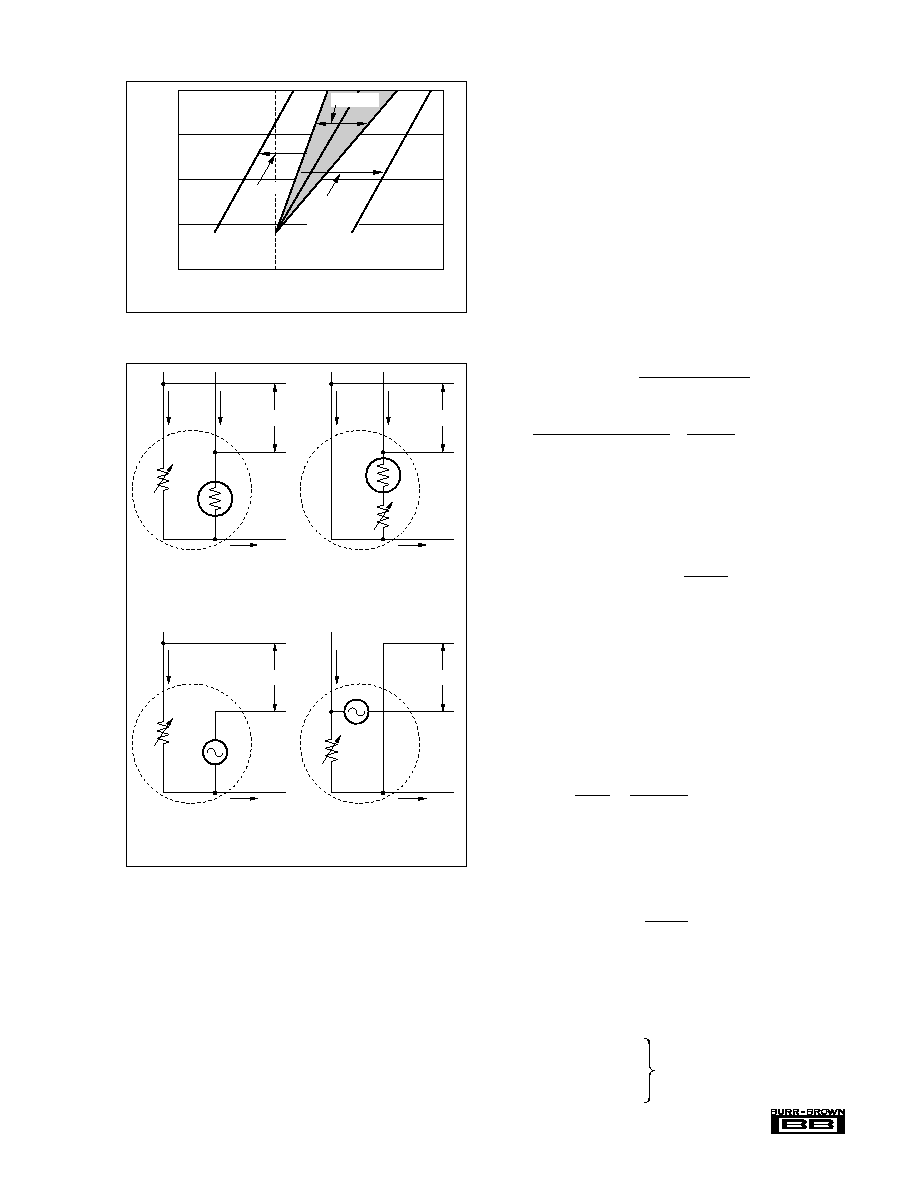
SIGNAL SUPPRESSION AND ELEVATION
In some applications it is desired to have suppressed zero
range (input signal elevation) or elevated zero range (input
signal suppression). This is easily accomplished with the
XTR101 by using the current sources to create the suppres-
sion/elevation voltage. The basic concept is shown in Fig-
ures 7 and 8(a). In this example the sensor voltage is derived
from R
T
(a thermistor, RTD, or other variable resistance
element) excited by one of the 1mA current sources. The
other current source is used to create the elevated zero range
voltage. Figures 8(b), (c) and (d) show some of the possible
circuit variations. These circuits have the desirable feature
of noninteractive span and suppression/elevation adjust-
ments. Note: It is not recommended to use the optional offset
voltage null (pins 1, 2 and 14) for elevation/suppression.
This trim capability is used only to null the amplifier's input
offset voltage. In many applications the already low offset
voltage (typically 20
µ
V) will not need to be nulled at all.
Adjusting the offset voltage to nonzero values will disturb
the voltage drift by
±
0.3
µ
V/
°
C per 100
µ
V or induced offset.
16mA/100mV) 0.016
40
0.144
40
0.16 0.016
40
40
I
O
/
e
IN
0.016
(1)
FIGURE 5. Basic Connection for Floating Voltage Source.
FIGURE 6. Basic Connection for Resistive Source.
+
8
10
11
3
5
6
4
R
S
e
IN
+
XTR101
R
2
2.5k
7
2mA
0.01µF
0.01µF
D
1
I
O
2
1
4-20 mA
e
1
e
2
R
L
Offset
Adjust
1M
e'
2
Adj.
2mA
+5V
I
O
= 4mA + (0.016 + )e
IN
R
S
40
e
IN
= e
2
+
14
e
L
+
24V
+
+
8
10
3
5
6
4
R
S
e
IN
+
XTR101
R
2
2.5k
7
1mA
0.01µF
D
1
2
1
e
1
e
2
Offset
Adjust
100k
e
2
2mA
+5V
I
O
= 4mA + (0.016 + )e
IN
R
S
40
e
IN
= e'
2
= 1mA
X
R
T
+
0.01µF
1mA
R
T
1M
11
Alternate circuitry
shown in Figure 8.
14
+
24V
+
R
L
e
L
®
XTR101
9
40
e
IN
e'
2
+
1mA
1mA
+
R
4
V
4
2mA
+
+
+
+
+
+
2mA
+
+
+
+
R
T
e'
2
R
T
e
IN
1mA
1mA
R
4
V
4
2mA
e'
2
R
4
V
4
e
IN
2mA
e
IN
2mA
2mA
e'
2
R
4
V
4
e
IN
= (e'
2
+V
4
)
V
4
= 1mA
X
R
4
e'
2
= 1mA
X
R
T
(b) Suppressed Zero Range
e
IN
= (e'
2
V
4
)
V
4
= 1mA
X
R
4
e'
2
= 1mA
X
R
T
(a) Elevated Zero Range
e
IN
= (e'
2
V
4
)
V
4
= 2mA
X
R
4
(c) Elevated Zero Range
e
IN
= (e'
2
+V
4
)
V
4
= 2mA
X
R
4
(d) Suppressed Zero Range
FIGURE 8. Elevation and Suppression Circuits.
APPLICATION INFORMATION
The small size, low offset voltage and drift, excellent linear-
ity, and internal precision current sources, make the XTR101
ideal for a variety of two-wire transmitter applications. It can
be used by OEMs producing different types of transducer
transmitter modules and by data acquisition systems manu-
facturers who gather transducer data. Current mode trans-
mission greatly reduces noise interference. The two-wire
nature of the device allows economical signal conditioning
at the transducer. Thus the XTR101 is, in general, very
suitable for individualized and special purpose applications.
EXAMPLE 1
RTD Transducer shown in Figure 9.
Given a process with temperature limits of +25
°
C and
+150
°
C, configure the XTR101 to measure the temperature
with a platinum RTD which produces 100
at 0
°
C and
200
at +266
°
C (obtained from standard RTD tables).
Transmit 4mA for +25
°
C and 20mA for +150
°
C.
COMPUTING R
S
:
The sensitivity of the RTD is
R/
T = 100
/266
°
C. When
excited with a 1mA current source for a 25
°
C to 150
°
C range
(i.e., 125
°
C span), the span of e
IN
is 1mA X (100
/266
°
C)
X 125
°
C = 47mV =
e
IN
.
From equation 1, R
S
=
R
S
=
=
= 123.3
Span adjustment (calibration) is accomplished by trimming
R
S
.
COMPUTING R
4
:
At +25
°
C, e'
2
= 1mA (R
T
+
R
T
)
= 1mA [100
+ X 25
°
C]
= 1mA (109.4
) = 109.4mV
In order to make the lower range limit of 25
°
C correspond
to the output lower range limit of 4mA, the input circuitry
shown in Figure 9 is used.
e
IN
, the XTR101 differential input, is made 0 at 25
°
C or
e'
2 25
°
C
V
4
= 0
thus, V
4
= e'
2 25
°
C
= 109.4mV
R
4
= = = 109.4
COMPUTING R
2
AND CHECKING CMV:
At +25
°
C, e'
2
= 109.4mV
At +150
°
C, e'
2
= 1mA (R
T
+
R
T
)
= 1mA [100
+( X 150
°
C)]
= 156.4mV
Since both e'
2
and V
4
are small relative to the desired 5V
common-mode voltage, they may be ignored in computing
R
2
as long as the CMV is met.
R
2
= 5V/2mA = 2.5k
e
2
min = 5V + 0.1094V
e
2
max = 5V + 0.1564V
e
1
= 5V + 0.1094V
I
O
/
e
IN
0.016
40
40
16mA/47mV 0.016
266
°
C
100
1mA
109.4mV
1mA
V
4
0.3244
266
°
C
100
The +4V to +6V CMV
requirement is met.
0 +
i
0
(mA)
20
15
10
5
0
Elevated
Zero
Range
Suppressed
Zero
Range
Span Adjust
e
IN
(V)
FIGURE 7. Elevation and Suppression Graph.
®
XTR101
10
FIGURE 10. Thermocouple Input Circuit with Two
Temperature Regions and Diode (D) Cold
Junction Compensation.
FIGURE 9. Circuit for Example 1.
EXAMPLE 2
Thermocouple Transducer shown in Figure 10.
Given a process with temperature (T
1
) limits of 0
°
C and
+1000
°
C, configure the XTR101 to measure the temperature
with a type J thermocouple that produces a 58mV change for
1000
°
C change. Use a semiconductor diode for a cold
junction compensation to make the measurement relative to
0
°
C. This is accomplished by supplying a compensating
voltage, V
R6
, equal to that normally produced by the thermo-
couple with its "cold junction" (T
2
) at ambient. At a typical
ambient of +25
°
C this is 1.28mV (obtained from standard
thermocouple tables with reference junction of 0
°
C). Trans-
mit 4mA for T
1
= 0
°
C and 20mA for T
1
= +1000
°
C. Note:
e
IN
= e
2
e
1
indicates that T
1
is relative to T
2
.
ESTABLISHING R
S
:
The input full scale span is 58mV (
e
INFS
= 58mV).
R
S
is found from equation (1)
R
S
=
=
= = 153.9
SELECTING R
4
:
R
4
is chosen to make the output 4mA at T
TC
= 0
°
C (V
TC
=
1.28mV) and T
D
= +25
°
C (V
D
= 0.6V). A circuit is shown
in Figure 10.
V
TC
will be 1.28mV when T
TC
= 0
°
C and the reference
junction is at +25
°
C. e
1
must be computed for the condition
of T
D
= +25
°
C to make e
IN
= 0V.
V
D 25
°
C
= 600mV
e
1 25
°
C
= 600mV (51/2051) = 14.9mV
e
IN
= e
2
e
1
= V
TC
+ V
4
e
1
40
40
40
16mA/58mV 0.016
I
O
/
e
IN
0.016
0.2599
q
KT
R
5
+ R
6
R
6
(2)
With e
IN
= 0 and V
TC
= 1.28mV,
V
4
= e
1
+ e
IN
V
TC
= 14.9mV + 0V (1.28mV)
1mA (R
4
) = 16.18mV
R
4
= 16.18
COLD JUNCTION COMPENSATION:
The temperature reference circuit is shown in Figure 11.
The diode voltage has the form
V
D
= ln
Typically at T
2
= +25
°
C, V
D
= 0.6V and
V
D
/
T =
2mV/
°
C. R
5
and R
6
form a voltage divider for the diode
voltage V
D
. The divider values are selected so that the
gradient
V
D/
T equals the gradient of the thermocouple at
the reference temperature. At +25
°
C this is approximately
52
µ
V/
°
C (obtained from standard thermocouple table);
therefore,
T
C
/
T =
V
D/
T
52
µ
V/
°
C = 2000
µ
V/
°
C
R
5
is chosen as 2k
to be much larger than the resistance of
the diode. Solving for R
6
yields 51
.
THERMOCOUPLE BURN-OUT INDICATION
In process control applications it is desirable to detect when
a thermocouple has burned out. This is typically done by
forcing the two-wire transmitter current to either limit when
I
DIODE
I
SAT
+
XTR101
1mA
1mA
R
6
51
+
2.5k
e
1
e
2
3
11
10
8
7
4
R
4
V
4
0.01µF
V
TC
Thermocouple
T
TC
Temperature T
1
Temperature T
2
= T
D
+
+
D
R
5
2k
e
IN
+
8
10
3
5
6
4
R
S
e
IN
+
XTR101
R
2
7
0.01µF
D
1
e
1
e
2
e'
2
+
0.01µF
R
T
11
V
4
R
4
+
+
24V
+
R
L
e
L
R
5
+ R
6
R
6
®
XTR101
11
FIGURE 11. Cold Junction Compensation Circuit.
V
5
1mA
R
5
+
V
6
R
6
+
V
D
+
D
FIGURE 12. Optional Filtering.
the thermocouple impedance goes very high. The circuits of
Figures 16 and 17 inherently have down scale indication.
When the impedance of the thermocouple gets very large
(open) the bias current flowing into the + input (large
impedance) will cause I
O
to go to its lower range limit value
(about 3.8mA). If up scale indication is desired the circuit of
Figure 18 should be used. When the T
C
opens the output will
go to its upper range limit value (about 25mA or higher).
OPTIONAL INPUT OFFSET VOLTAGE TRIM
The XTR101 has provisions for nulling the input offset
voltage associated with the input amplifiers. In many appli-
cations the already low offset voltages (30
µ
V max for the B
grade, 60
µ
V max for the A grade) will not need to be nulled
at all. The null adjustment can be done with a potentiometer
at pins 1, 2 and 14 as shown in Figures 5 and 6. Either of
these two circuits may be used. NOTE: It is not recom-
mended to use this input offset voltage nulling
capability for
elevation or suppression. See the Signal Suppression and
Elevation section for the proper techniques.
OPTIONAL BANDWIDTH CONTROL
Low-pass filtering is recommended where possible and can
be done by either one of two techniques shown in Figure 12.
C
2
connected to pins 3 and 4 will reduce the bandwidth with
a cutoff frequency given by,
f
CO
=
This method has the disadvantage of having f
CO
vary with
R
1
, R
2
, R
3
, R
4
, and it may require large values of R
3
and R
4
.
The other method, using C
1
, will use smaller values of
capacitance and is not a function of the input resistors. It is,
however, more subject to nonlinear distortion caused by
slew rate limiting. This is normally not a problem with the
slow signals associated with most process control transduc-
ers. The relationship between C
1
and f
CO
is shown in the
Typical Performance Curves.
(R
1
+ R
2
+ R
3
+ R
4
) (C
2
+ 3pF)
15.9
FIGURE 13. 0-20mA Output Converter.
APPLICATION CIRCUITS
3
4
+
XTR101
1mA
13
12
NOTE: (1) R
3
and R
4
should be equal if used.
1mA
R
2
11
0.0047µF
C
1
R
4
(1)
R
3
(1)
C
2
R
1
Gain
e
2
OUTPUT STAGE
Internally e
NOISE RTI
= e
2
INPUT STAGE
+
2
XTR101
R
2
500
100pF
MC1403A
OPA27
V
R
= 2.5V
+
V
V+
I
O
(4-20mA)
I
O
(1)
(0-20mA)
R
1
125
NOTE: (1) I
O
=
1 + I
O
= 1.25 I
O
5mA
R
1
R
2
V
R
R
2
Other conversions are readily achievable by
changing the reference and ratio of R
1
to R
2
.
Voltage
Reference
®
XTR101
12
FIGURE 14. Bridge Input, Voltage Excitation.
FIGURE 15. Bridge Input, Current Excitation.
FIGURE 16. Thermocouple Input with RTD Cold Junction
Compensation.
FIGURE 17. Thermocouple Input with Diode Cold Junction
Compensation.
FIGURE 18. Thermocouple Input with RTD Cold Junction
Compensation.
+
R
S
+
XTR101
2.5k
1mA
20
51
Zero
Adjust
1mA
This circuit has down
scale burn-out indication.
Type J
2k
R
S
+
XTR101
2.5k
1mA
RTD
100
20
15
+
1mA
This circuit has up
scale burn-out indication.
Zero
Adjust
2mA
XTR101
R
R
R
R
S
300
2.2k
R
J
+
+
R
S
+
XTR101
2.5k
1mA
RTD
100
20
Zero
Adjust
15
1mA
This circuit has down
scale burn-out indication.
Type J
2mA
+
XTR101
0.9852mA
1.0147mA
R
R
R
R
S
1.8k
300
4.7k
0.01µF
LM129
6.9V
Voltage
Ref
R
®
XTR101
13
FIGURE 19. Dual Precision Current Sources Operated From One Supply.
FIGURE 20. Isolated Two-Wire Current Loop.
7
+
XTR101
4-20mA
8
7
+
10
12
18
16
+V
2
722
V
2
C
2
C
1
V
1
+V
1
P+
E
V+
V
2
4 3
8
ISO100
I
REF2
1M
1M
250
1k
Isolation
Barrier
1µF
1µF
+15V
15V
V
OUT
(1)
+1V to +5V
NOTE: (1) Can be shifted and amplified
using ISO100 current sources.
I
REF1
30V
+
e
IN
+15V
9
17
15
R
1
+
2.5k
11
10
OPA21
8
7
3
4
0.01µF
15V
+V
CC
R
2
I
1
I
2
+V
CC
V
REF
= ImA R
2
XTR101
V
REF
Out

®
XTR101
14
(9)
20.40
µ
A
16mA
(10)
40
R
S
123.3
40
3.16 X 10
5
2120mV
3.16 X 10
3
0.1092V
CMRR
(
e
1
+ e
2
)/2 5V
V
CC
PSRR
DETAILED ERROR ANALYSIS
The ideal output current is
i
O IDEAL
= 4mA + K e
IN
K is the span (gain) term, (0.016
+ (40/R
S
)) (3)
In the XTR101 there are three major components of error:
1.
O
= errors associated with the output stage.
2.
S
= errors associated with span adjustment.
3.
I
= errors associated with the input stage.
The transfer function including these errors is
i
O
ACTUAL
= (4mA +
O
) + K (1 +
S
)(e
IN
+
I
) (4)
When this expression is expanded, second order terms
(
S
1
) dropped, and terms collected, the result is
i
O
ACTUAL
= (4mA +
O
) + K e
IN
+ K
I
+ K
S
e
IN
(5)
The error in the output current is i
O
ACTUAL
i
O IDEAL
and
can be found by subtracting equations (5) and (3).
i
O ERROR
=
O
+ K
1
+ K
S
e
IN
(6)
This is a general error expression. The composition of each
component of error depends on the circuitry inside the
XTR101 and the particular circuit in which it is applied. The
circuit of Figure 9 will be used to illustrate the principles.
1.
O
= I
OS RTO
(7)
2.
S
=
NONLINEARITY
+
SPAN
(8)
3.
I
= V
OSI
+ (I
B1
+ R
4
I
B2
R
T
) +
+
The term in parentheses may be written in terms of offset
current and resistor mismatches as I
B1
R + I
OS
' R
4
.
V
OSI
* = input offset voltage
I
B1
*, I
B2
* = input bias current
I
OSI
* = input offset current
I
OS RTO
* = output offset current error
R = R
T
R
4
= mismatch in resistor
V
CC
= change supply voltage between
pins 7 and 8 away from 24V nominal
PSRR* = power supply rejection ratio
CMRR* = common-mode rejection ratio
NONLIN
* = span nonlinearity
SPAN
* = span equation error. Untrimmed error
= 5% max. May be trimmed to zero.
Items marked with an asterisk (*) can be found in the
Electrical Specifications.
EXAMPLE 3
The circuit in Figure 9 with the XTR101BG specifications
and the following conditions: R
T
= 109.4
at 25
°
C, R
T
=
156.4
at 150
°
C, I
O
= 4mA at 25
°
C, I
O
= 20mA at 150
°
C,
R
S
= 123.3
, R
4
= 109
, R
L
= 250
, R
LINE
= 100
, V
DI
=
0.6V, V
PS
= 24V
±
0.5%. Determine the % error at the upper
and lower range values.
(
e
1
+ e
2
)/2 5V
CMRR
A. AT THE LOWER RANGE VALUE (T = +25
°
C).
O
= I
OS RTO
=
±
6
µ
A
I
= V
OSI
+ (I
B1
R + I
OS1
R
4
) +
+
R = R
T 25
°
C
R
4
= 109.4 109
0
V
CC
= (24 X 0.005) + 4mA (250
+ 100
) + 0.6V
= 120mV + 1400mV + 600mV
= 2120mV
e
1
= (2mA X 2.5k
) + (1mA X 109
) = 5.109V
e
2
= (2mA X 2.5k
) + (1mA X 109.4
)
= 5.1094V
(e
1
+ e
2
)/2 5 = 0.1092V
PSRR = 3.16 X 10
5
for 110dB
CMRR = 31.6 X 10
3
for 90dB
1
= 30
µ
V + (150nA X 0 + 20nA X 109
)
+ +
= 30
µ
V + 2.18
µ
V + 6.7
µ
V + 3.46
µ
V
= 42.34
µ
V
S
=
NONLIN
+
SPAN
= 0.0001 + 0 (assumes trim of R
S
)
I
O
error =
O
+ K
I
+ K
S
e
IN
K = 0.016 + = 0.016 + = 0.340
e
IN
= e
2
V
4
= I
REF1
R
T 25
°
C
I
REF2
R
4
since R
T 25
°
C
= R
4
,
e
IN
= (I
REF1
I
REF2
) R
4
= 0.4
µ
A X 109
= 43.6
µ
V
Since the maximum mismatch of the current references is
0.04% of 1mA = 0.4
µ
A,
I
O
error = 6
µ
A + (0.34 X 42.34
µ
V) + (0.34 X
0.0001 X 43.6
µ
V) = 6
µ
A + 14.40
µ
A + 0.0015
µ
A
= 20.40
µ
A
% error = X 100%
0.13% of span at lower range value.
B. AT THE UPPER RANGE VALUE (T = +150
°
C).
R = R
T 150
°
C
R
4
= 156.4 109.4 = 47
V
CC
= (24 X 0.005) + 20mA (250
+ 100
) +
0.6V = 7720mV
e
1
= 5.109V
e
2
= (2mA X 2.5k
) + (1mA X 156.4
) = 5.156V
(e
1
+ e
2
)/2 5V = 0.1325V
V
CC
PSRR

®
XTR101
15
0.1325V
3.16 X 10
5
7720mV
3.16 X 10
3
30.52
µ
A
16mA
O
= 6
µ
A
1
= 30
µ
V + (150nA X 47
+ 20nA X 190
)
+ +
= 30
µ
V + 9.23
µ
V + 24
µ
V + 4.19
µ
V
= 67.42
µ
V
S
= 0.0001
e
IN
= e'
2
V
4
= I
REF1
R
T 150
°
C
I
REF2
R
4
= (1mA X 156.4
) (1mA X 109
) = 47mV
I
O
error =
O
+ K
I
+ K
S
e
IN
= 6
µ
A +
(0.34
X 67.42
µ
V) + (0.34
X 0.0001
X 47000
µ
V) = 6
µ
A + 22.92
µ
A + 1.60
µ
A
= 30.52
µ
A
% error = X 100%
= 0.19% of span at upper range value.
CONCLUSIONS
Lower Range: From equation (10) it is observed that the
predominant error term is the input offset voltage (30
µ
V for
the B grade). This is of little consequence in many applica-
tions. V
OS
RTI
can, however, be nulled using the pot shown
in Figures 5 and 6. The result is an error of 0.06% of span
instead of 0.13% if span.
Upper Range: From equation (11), the predominant errors
are I
OS
RTO
(6
µ
A), V
OS RTI
(30
µ
V), and I
B
(150nA), max, B
grade. Both I
OS
and V
OS
can be trimmed to zero; however,
the result is an error of 0.09% of span instead of 0.19% span.
RECOMMENDED HANDLING
PROCEDURES FOR INTEGRATED CIRCUITS
All semiconductor devices are vulnerable, in varying
degrees, to damage from the discharge of electrostatic
energy. Such damage can cause performance degradation or
failure, either immediate or latent. As a general practice, we
recommend the following handling procedures to reduce the
risk of electrostatic damage.
1. Remove the static-generating materials, such as untreated
plastic, from all areas that handle microcircuits.
2. Ground all operators, equipment, and work stations.
3. Transport and ship microcircuits, or products incorporat
ing microcircuits, in static-free, shielded containers.
4. Connect together all leads of each device by means of a
conductive material, when the device is not connected
into a circuit.
5. Control relative humidity to as high a value as practical
(50% recommended).