A
11 to 17 Watt SD Single Series DC/DC Converters
Manufacturing Company, Inc. ∑ Concord, California 94520 ∑ Ph: 925/687-4411 or 800/542-3355 ∑ Fax: 925/687-3333 ∑ www.calex.com ∑ Email: sales@calex.com
1
eco# 041007-1
Features
Power Density of up to 25 Watts
Per Cubic Inch
Only 1 Square Inch of PCB Area Required
Efficiencies to >90%
Low Noise Outputs, 60 mV P-P Typical
Water Washable Case
Surface Mount Package Available
Five Year Warranty
Description
The SD single series breaks new ground on several fronts.
First is their power density of up to 25 watts per cubic inch. The
second is the operating efficiency that can exceed 90%.
The outputs are 3.3 and 5 volts with 5 volt or 6-15.5 volt
inputs respectively. This makes these converters ideal for
logic powered 3.3 volt down conversion or battery operation
of the more traditional 5 volt logic powered systems.
Coupled with this is the very low output noise of typically
less than 60 mV peak to peak. The noise is also fully specified
for RMS value and if even these impressive noise figures
aren't enough, our applications section shows a simple add
on circuit that can reduce the output noise to less than 20 mV
P-P.
The traditional flat package design has been stood on end
so that it takes up only 1 square inch of PCB area. No extra
heatsinking is required for most applications saving you
design time and valuable PCB space.
What all this means to you is a tighter, more compact
overall system. Full application information is provided to
make integrating this supply in your system a snap.
A remote ON/OFF function is included that places the
converter in a very low power state.
As with all CALEX converters the SD Single series is
covered by our 5 Year Warranty.
11-17 Watt SD Single Series Block Diagram
t
r
a
h
C
n
o
i
t
c
e
l
e
S
l
e
d
o
M
e
g
n
a
R
t
u
p
n
I
C
D
V
t
u
p
t
u
O
C
D
V
t
u
p
t
u
O
A
m
n
i
M
x
a
M
D
S
0
0
5
3
.
3
S
5
5
.
4
6
3
3
.
3
0
0
5
3
D
S
0
0
5
3
.
5
S
2
1
5
.
6
5
.
5
1
0
0
.
5
0
0
5
3

A
11 to 17 Watt SD Single Series DC/DC Converters
Manufacturing Company, Inc. ∑ Concord, California 94520 ∑ Ph: 925/687-4411 or 800/542-3355 ∑ Fax: 925/687-3333 ∑ www.calex.com ∑ Email: sales@calex.com
2
eco# 041007-1
NOTES
*
All parameters measured at Tc = 25∞C, nominal input voltage
and full rated load unless otherwise noted. Refer to the
CALEX Application Notes for the definition of terms,
measurement circuits and other information.
(1)
Noise is measured per CALEX application notes. Measurement
bandwidth is 0-20 MHz. RMS noise is measured over a 0.01-1
MHz bandwidth. To simulate standard PCB decoupling practices,
output noise is measured with a 1uF tantalum and 0.01µF
ceramic capacitor located 1 inch away from the converter.
(2)
See our application note for picking the correct fuse size.
(3)
The worst case output voltage includes line, load and temperature
effects.
(4)
Dynamic response of the converter will degrade when the SD
series is operated with less than 25% load.
(5)
Short term stability is defined as the drift over 24 hours with
constant line, load and ambient temperature conditions.
(6)
Transient response is specified for a 50 to 75% step load
change. Rise time of step is 2 microseconds.
(7)
Dynamic response is the peak overshoot for a transient as
described in note 6.
(8)
The functional temperature range is intended to give an additional
data point for use in evaluating this power supply. At the
low functional temperature the power supply will function with
no side effects, however, sustained operation at the high
functional temperature will reduce expected operational life.
The data sheet specifications are not guaranteed over the
functional temperature range.
(9)
The case thermal impedance is specified as the case temperature
rise over ambient per package watt dissipated.
(10) Water Washability - Calex DC/DC converters are designed to
withstand most solder/wash processes. Careful attention should
be used when assessing the applicability in your specific
manufacturing process. Converters are not hermetically sealed.
*
s
r
e
t
e
m
a
r
a
P
t
u
p
n
I
l
e
d
o
M
D
S
0
0
5
3
.
3
S
5
D
S
0
0
5
3
.
5
S
2
1
s
t
i
n
U
e
g
n
a
R
e
g
a
t
l
o
V
N
I
M
X
A
M
5
.
4
0
.
6
5
.
6
5
.
5
1
C
D
V
d
a
o
L
ll
u
F
t
n
e
r
r
u
C
t
u
p
n
I
d
a
o
L
o
N
P
Y
T
P
Y
T
5
1
6
2
1
5
3
6
1
1
A
m
y
c
n
e
i
c
i
f
f
E
P
Y
T
6
8
8
8
%
y
c
n
e
u
q
e
r
F
g
n
i
h
c
t
i
w
S
P
Y
T
0
0
1
z
H
k
,
e
g
a
t
l
o
v
r
e
v
O
t
u
p
n
I
m
u
m
i
x
a
M
m
u
m
i
x
a
M
s
m
0
0
2
X
A
M
5
.
7
0
.
7
1
C
D
V
,
e
m
i
T
n
o
-
n
r
u
T
r
o
r
r
E
t
u
p
t
u
O
%
1
P
Y
T
0
0
2
0
1
s
m
e
s
u
F
d
e
d
n
e
m
m
o
c
e
R
)
2
(
S
P
M
A
*
s
r
e
t
e
m
a
r
a
P
t
u
p
t
u
O
l
e
d
o
M
D
S
0
0
5
3
.
3
S
5
D
S
0
0
5
3
.
5
S
2
1
s
t
i
n
U
e
g
a
t
l
o
V
t
u
p
t
u
O
3
3
.
3
0
0
.
5
C
D
V
)
3
(
y
c
a
r
u
c
c
A
e
g
a
t
l
o
V
t
u
p
t
u
O
e
s
a
C
t
s
r
o
W
N
I
M
P
Y
T
X
A
M
0
0
2
.
3
0
3
3
.
3
0
9
3
.
3
0
0
8
.
4
0
0
0
.
5
0
5
2
.
5
C
D
V
)
4
(
e
g
n
a
R
d
a
o
L
d
e
t
a
R
N
I
M
X
A
M
0
0
0
5
3
A
m
n
o
i
t
a
l
u
g
e
R
d
a
o
L
d
a
o
L
x
a
M
-
d
a
o
L
x
a
M
%
5
2
P
Y
T
X
A
M
7
.
1
5
.
2
%
n
o
i
t
a
l
u
g
e
R
e
n
i
L
C
D
V
x
a
M
-
n
i
M
=
n
i
V
P
Y
T
X
A
M
2
.
0
0
.
1
4
.
0
0
.
1
%
)
5
(
y
t
il
i
b
a
t
S
m
r
e
T
t
r
o
h
S
P
Y
T
1
0
.
0
<
s
r
H
4
2
/
%
y
t
il
i
b
a
t
S
m
r
e
T
g
n
o
L
P
Y
T
1
.
0
<
5
0
.
0
<
s
r
H
k
/
%
)
6
(
e
s
n
o
p
s
e
R
t
n
e
i
s
n
a
r
T
P
Y
T
0
0
1
0
0
2
s
µ
)
7
(
e
s
n
o
p
s
e
R
c
i
m
a
n
y
D
P
Y
T
0
5
5
7
k
a
e
p
V
m
)
1
(
k
a
e
P
-
k
a
e
P
,
e
s
i
o
N
P
Y
T
0
4
0
6
P
-
P
V
m
e
s
i
o
N
S
M
R
P
Y
T
5
8
S
M
R
V
m
t
n
e
i
c
i
f
f
e
o
C
e
r
u
t
a
r
e
p
m
e
T
P
Y
T
X
A
M
0
5
0
5
1
C
∞
/
m
p
p
n
o
m
m
o
C
o
t
n
o
i
t
c
e
t
o
r
P
t
i
u
c
r
i
C
t
r
o
h
S
t
i
m
i
L
t
n
e
r
r
u
C
s
u
o
u
n
i
t
n
o
C

A
11 to 17 Watt SD Single Series DC/DC Converters
Manufacturing Company, Inc. ∑ Concord, California 94520 ∑ Ph: 925/687-4411 or 800/542-3355 ∑ Fax: 925/687-3333 ∑ www.calex.com ∑ Email: sales@calex.com
3
eco# 041007-1
n
i
P
n
o
i
t
c
n
u
F
n
i
P
n
o
i
t
c
n
u
F
1
F
F
O
/
N
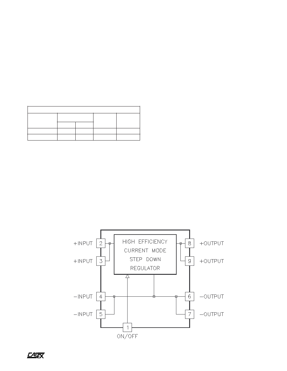
O
6
T
U
P
T
U
O
-
2
T
U
P
N
I
+
7
T
U
P
T
U
O
-
3
T
U
P
N
I
+
8
T
U
P
T
U
O
+
4
T
U
P
N
I
-
9
T
U
P
T
U
O
+
5
T
U
P
N
I
-
FRONT VIEW
RIGHT VIEW
Applications Information
You truly get what you pay for in a CALEX converter, a
complete system oriented and specified DC/DC converter -
no surprises, no component selection problems, no heatsinking
problems, just "plug and play".
The SD Single series like all CALEX converters carries the
full 5 year CALEX no hassle warranty. We can offer a five year
warranty where others can't because with CALEX it's rarely
needed.
Keep reading, you'll find out why.
General Information
The 100 kHz operating frequency of the SD Single series
allows an increased power density of up 25 watts per cubic
inch while still including adequate heat sinking and full filtering
on both the input and output. This prevents the need for
additional filtering and heatsinking in most applications.
The series is also mindful of battery operation for industrial,
medical control and remote data collection applications. The
remote ON/OFF pin places the converter in a very low power
mode that draws typically less than 5 µA from the input source.
Noise has also achieved new lows in this single design,
while the industry standard is to specify output noise as 1 to
5% peak to peak typical with no mention of measurement
bandwidth. The SD converters achieve 60 mV peak to peak
typical and are fully specified and tested to a wide bandwidth
of 0-20 MHz.
Full overload protection is provided by independent pulse-
by-pulse current limiting. This protection scheme assures you
that our SD single will provide you with zero failure rate
operation.
A non-conductive / water washable case is standard along
with specified operation over the full industrial temperature
range of -40 to +85∞C case temperature.
Applying The Input
Figure 1 shows the recommended input connections for the
SD Single DC/DC converter. A fuse is recommended to
protect the input circuit and should not be omitted. The fuse
serves to prevent unlimited current from flowing in the case of
a catastrophic system failure.
Figure 1.
Standard connections for the SD single input. The ON/OFF pin must
be connected to common for proper operation. The input protection
fuse should not be omitted. See the text for suggestions regarding
C1 and C2.
Mechanical tolerances unless
otherwise noted:
X.XX dimensions: ±0.020 inches
X.XXX dimensions: ±0.005 inches
*
s
n
o
i
t
a
c
i
f
i
c
e
p
S
l
a
r
e
n
e
G
s
l
e
d
o
M
l
l
A
s
t
i
n
U
n
o
i
t
c
n
u
F
F
F
O
/
N
O
l
e
v
e
L
c
i
g
o
L
F
F
O
n
e
p
O
n
i
P
e
v
a
e
L
r
o
N
I
M
0
.
2
>
C
D
V
l
e
v
e
L
c
i
g
o
L
N
O
t
u
p
n
I
-
o
t
n
i
P
e
i
T
r
o
X
A
M
5
.
0
<
C
D
V
e
g
a
t
l
o
V
m
u
m
i
x
a
M
X
A
M
3
.
0
+
n
i
V
C
D
V
t
n
e
r
r
u
C
e
l
d
I
r
e
t
r
e
v
n
o
C
h
g
i
H
n
i
P
F
F
O
/
N
O
P
Y
T
5
A
µ
l
a
t
n
e
m
n
o
r
i
v
n
E
e
g
n
a
R
g
n
i
t
a
r
e
p
O
e
s
a
C
g
n
i
t
a
r
e
D
o
N
N
I
M
X
A
M
0
4
-
5
8
C
∞
)
8
(
e
g
n
a
R
l
a
n
o
i
t
c
n
u
F
e
s
a
C
N
I
M
X
A
M
0
5
-
5
9
C
∞
e
g
n
a
R
e
g
a
r
o
t
S
N
I
M
X
A
M
5
5
-
5
0
1
C
∞
)
9
(
e
c
n
a
d
e
p
m
I
l
a
m
r
e
h
T
P
Y
T
0
2
t
t
a
W
/
C
∞
t
h
g
i
e
W
t
i
n
U
P
Y
T
0
.
1
z
o

A
11 to 17 Watt SD Single Series DC/DC Converters
Manufacturing Company, Inc. ∑ Concord, California 94520 ∑ Ph: 925/687-4411 or 800/542-3355 ∑ Fax: 925/687-3333 ∑ www.calex.com ∑ Email: sales@calex.com
4
eco# 041007-1
When using the SD Single be sure that the impedance at
the input to the converter is less than about 0.075 ohms from
DC to about 100 kHz, this is usually not a problem in battery
powered systems when the converter is connected directly to
the battery. If the converter is located more than about 2
inches from the input source an added capacitor may be
required directly at the input pins for proper operation.
The maximum source impedance is a function of output
power and line voltage. The impedance can be higher when
operating at less than full power. The required impedance
reduces as the input voltage is raised or the power is reduced.
In general you should keep the voltage measured across the
input pins less than 0.2 volts peak to peak (not including any
high frequency spikes) for maximum converter performance
and life.
There is no lower limit on the allowed source impedance,
it can be any physically realizable value, even approaching
zero.
If the source impedance is too large in your system you
should choose an external input capacitor as detailed below.
Picking An External Input Capacitor
Several system tradeoffs must be made for each particular
system application to correctly size the input capacitor.
The probable result of undersizing the capacitor is increased
self heating, shortening it's life. Oversizing the capacitor can
have a negative effect on your products cost and size,
although this kind of overdesign does not result in shorter life
of any components.
There is no one optimum value for the input capacitor. The
size and capacity depend on the following factors:
1) Expected ambient temperature and your derating
guidelines.
2) The maximum anticipated load on the converter.
3) The input operating voltage, both nominal and excursions.
4) The statistical probability that your system will spend a
significant time at any worst case extreme.
Factor 1 depends on your system design guidelines.
These can range from 50 to 100% of the manufacturers listed
maximum rating, although the usual derating factor applied is
about 70%.
Factors 2 and 3 realistically determine the worst case ripple
current rating required for the capacitor.
Factor 4 is not easy to quantify. At CALEX we can make no
assumptions about a customers system so we leave to you
the decision of how you define how big is big enough.
Suggested Input Capacitor Sources
These capacitors may be used to lower your sources input
impedance at the input of the converter. These capacitors will
work for 100% load, worst case input voltage and ambient
temperature extremes. They however, may be oversized for
your exact usage. You may also use several smaller capacitors
in parallel to achieve the same ripple current rating. This may
save space in some systems.
Lowest Cost:
United Chemi-Con
SXE, RXC, RZ and RZA series
Suggested Part:
SXE016VB681M12.5X15LL
680µF, 16V, 105∞C RATED
ESR=0.12 OHMS
Allowable Ripple at 85∞C = 1.7 A
Panasonic
HFG and HFQ Series
Suggested Part:
ECA1CFG102
1000µF, 16V, 105∞C RATED
ESR=0.076 OHMS
Allowable Ripple at 85∞C = 1.6 A
Smallest Size:
Sprague/Vishay
195D Series (SMT)
Suggested Part:
195D686X0016R2T
68µF, 16V, 125∞C RATED
ESR=0.2 OHMS (maximum)
Allowable Ripple at 85∞C = 1.1 A
Applying The Output
Figure 1 shows typical output connections for the SD single.
The specified capacitor should be used for improved dynamic
performance. The capacitance can be a low cost aluminum
electrolytic type and can be broken up or "Distributed" around
your circuit.
The ESR requirements of the output capacitance are not
particularly stringent. Any capacitor with an ESR of less than
about 0.7 ohms will work well. Use the low cost / general
purpose types for maximum cost effectiveness. The use of a
high performance / low ESR type will help to reduce the high
frequency noise and add extra stability at light loads.
Suggested Output Capacitor Sources
These capacitors will work for 100% load, worst case input
voltage and ambient temperature extremes. They however,
may be oversized for your exact usage. You may also use
several smaller capacitors in parallel to achieve the same
capacitance rating. This may save space in some systems.
United Chemi-Con
KME, KMC and KRG series
Suggested Part:
KRG6.3VB102M12.5X12.5LL
1000µF, 6.3V, 105∞C Rated
Nichicon
VZ and VX series
Suggested Part:
UVZ0J102MPH
1000µF, 6.3V, 105∞C Rated
Panasonic
NHE and NXS Series
Suggested Part:
ECEA0JGE102
1000µF, 6.3V, 105∞C Rated

A
11 to 17 Watt SD Single Series DC/DC Converters
Manufacturing Company, Inc. ∑ Concord, California 94520 ∑ Ph: 925/687-4411 or 800/542-3355 ∑ Fax: 925/687-3333 ∑ www.calex.com ∑ Email: sales@calex.com
5
eco# 041007-1
Remote ON/OFF Pin Operation
The remote ON/OFF pin should be tied to -Input if this function
is not used. The best way to drive this pin is with a CMOS or
TTL gate. An open collector or relay contact may also be used
in conjunction with a 2.2 to 50 kohm resistor tied to +Input.
When the ON/OFF pin is high with respect to the -Input, the
converter is placed in a low power drain state. The ON/OFF
pin turns the converter off while keeping the input bulk
capacitor fully charged. This prevents the large inrush current
spike that occurs when the +input pin is opened and closed.
The OFF state current is typically less than 5 µA. Leakage
in external components may increase this value.
Temperature Derating
The SD Single series can operate up to 85∞C case temperature
without derating. Case temperature may be roughly calculated
from ambient by knowing that the SD Singles case temperature
rise is approximately 20∞C per package watt dissipated.
For example: If a 12S5.3500SD converter is outputting 10
Watts, at what ambient could it expect to run with no moving
air and no extra heatsinking?
Efficiency is approximately 90%, this leads to an input
power of 11 watts. The case temperature rise would be 1 watt
◊ 20 = 20∞C. This number is subtracted from the maximum
case temperature of 85∞C to get: 65∞C.
This example calculation is for an SD single without any
extra heat sinking or appreciable air flow. Both of these factors
can greatly effect the maximum ambient temperature (see
below). Exact efficiency depends on input line and load
conditions, check the efficiency curves for exact information.
This is a rough approximation to the maximum ambient
temperature. Because of the difficulty of defining ambient
temperature and the possibility that the loads dissipation may
actually increase the local ambient temperature significantly,
these calculations should be verified by actual measurement
before committing to a production design.
Heat sinking action can be improved by forced air over the
length of the converter or by using the SMT package and
placing the SD flat against a copper ground plane. The use of
a thin structural adhesive or thermal epoxy can increase the
heat conduction into the ground plane.
A heat sink can also be clamped or thermally glued to the
length of the SD. Suitable heat sinks made for DIL IC packages
can reduce the thermal impedance by 50% or more with
forced air.
Ultra Low Noise Output Circuit
The circuit shown in figure 2 can be used to reduce the output
noise to below 20 mV P-P over a 20 MHz bandwidth. Size
inductor L1 appropriately for the maximum expected load
current. C1 and C2 are United Chemi-Con 1200µF, 6.3 volt
SXE types or equivalent.
Figure 2.
For very low noise applications this circuit will reduce the output
noise to less than 20 mV P-P over a 0-20 MHz bandwidth. Be sure
to size the inductor appropriately for the maximum expected load
current.
Operation With Very Light Loads
At output loads less than about 25% of rated load, the SD
single will operate in a "Burst Mode". That is the SD will cease
PWM operation and instead operate in more of a burst mode.
This mode significantly increases the light load efficiency of
the SD single. Under these conditions the output of the SD will
contain a larger than normal (compared to full load) output
noise, but at a lower frequency.
If this is a problem in your application the SD single may be
used with a dummy load resistor to keep the static output
current above about 25% load (check the exact value required
by your circuit). Another alternative is to connect an inexpensive
1000 to 10,000 µF output capacitor with an ESR of 0.075 to 1
ohm to the output. This will help to dampen the low frequency
output ripple without upsetting the dynamic operation of the
SD.
Perhaps the best solution to the "No Load" condition is to
use the ON/OFF pin to control no load operation and shut the
converter down totally.
Dynamic response of the SD single will degrade when the
unit is operated with less than 25% of full rated power.
Grounding
The input and output sections are connected together internally
(not isolated). The best way to operate the converter is by
using the -Input and -Output pins independently. That is the
input source to output circuit connections should be through
the converter itself. This is shown in figure 1. The converter
may also be operated with the -Input and -Output pins
connected to a common ground plane. This can create an
"Extra" ground loop and may increase the output noise
depending on the impedance of the extra loop.
L1
= 30µH / 3.5 AMP INDUCTOR
C1, C2
= SEE TEXT

A
11 to 17 Watt SD Single Series DC/DC Converters
Manufacturing Company, Inc. ∑ Concord, California 94520 ∑ Ph: 925/687-4411 or 800/542-3355 ∑ Fax: 925/687-3333 ∑ www.calex.com ∑ Email: sales@calex.com
6
eco# 041007-1
Typical Performance (Tc=25∞C, Vin=Nom VDC, Rated Load).
4.0
4.5
5.0
5.5
6.0
LINE INPUT(VOLTS)
70
75
80
85
90
95
EFFICIENCY(%)
3.3 VOLT EFFICIENCY Vs. LINE INPUT VOLTAGE
100% FULL LOAD
50% FULL LOAD
0
10
20
30
40
50
60
70
80
90
100
LOAD (%)
70
75
80
85
90
95
EFFICIENCY (%)
3.3 VOLT EFFICIENCY Vs. LOAD
0
1
2
3
4
5
6
LINE INPUT (VOLTS)
0.0
0.5
1.0
1.5
2.0
2.5
3.0
3.5
INPUT CURRENT (AMPS)
3.3 VOLT INPUT CURRENT Vs. LINE INPUT VOLTAGE
100% LOAD
50% LOAD
0
10
20
30
40
50
60
70
80
90
100
LOAD (%)
70
75
80
85
90
95
EFFICIENCY (%)
5.0 VOLT EFFICIENCY Vs. LOAD
6
7
8
9
10
11
12
13
14
15
LINE INPUT(VOLTS)
70
75
80
85
90
95
EFFICIENCY(%)
5.0 VOLT EFFICIENCY Vs. LINE INPUT VOLTAGE
100% FULL LOAD
50% FULL LOAD
0
2
4
6
8
10
12
14
16
LINE INPUT (VOLTS)
0.0
0.5
1.0
1.5
2.0
2.5
3.0
3.5
INPUT CURRENT (AMPS)
5.0 VOLT INPUT CURRENT Vs. LINE INPUT VOLTAGE
100% LOAD
50% LOAD