 | –≠–ª–µ–∫—Ç—Ä–æ–Ω–Ω—ã–π –∫–æ–º–ø–æ–Ω–µ–Ω—Ç: 12T5.15LE | –°–∫–∞—á–∞—Ç—å:  PDF PDF  ZIP ZIP |
A
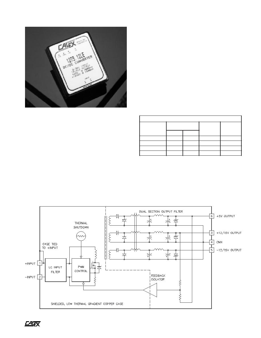
27 to 30 Watt LE Triple Series DC/DC Converters
2401 Stanwell Drive ∑ Concord, California 94520 ∑ Ph: 925/687-4411 or 800/542-3355 ∑ Fax: 925/687-3333 ∑ www.calex.com ∑ Email: sales@calex.com
1
3/2001, eco# 041007-1
Features
Triple Output
Wide 4:1 Input Voltage Range
(9-36 or 18-72 VDC)
High Efficiency, up to 85%
No Derating to 85∞C Case Temperature
LC Input Filter, Dual Section Output Filters
PCB Mounting With Optional Heat Sink and
Chassis Mounting Kit
Five Year Warranty
Description
The 4:1 input range of the LE Triple Series makes them ideal
for a wide variety of power requirements including battery and
unregulated input applications. Each converter's +5V is
tightly regulated and useful for driving standard logic circuits.
These 27-30 Watt converters have dual output filters. They
provide a low output noise of 50 mV P-P typical and are fully
specified and tested to the maximum specifications. Input
filtering significantly reduces the reflected ripple noise.
Unlike comparable converters, all inputs and outputs are
protected from transient overvoltage conditions. Overload
protection is provided by current sensing of the primary
switching current and an independent thermal sensor. The
27-30 Watt Triple Series, like all CALEX converters, carries
the full 5 Year CALEX Warranty.
27-30 Watt Triple Series Block Diagram
t
r
a
h
C
n
o
i
t
c
e
l
e
S
l
e
d
o
M
e
g
n
a
R
t
u
p
n
I
C
D
V
s
t
u
p
t
u
O
C
D
V
s
t
u
p
t
u
O
A
m
n
i
M
x
a
M
E
L
2
1
.
5
T
2
1
9
6
3
2
1
±
,
5
0
0
5
±
,
0
0
0
3
E
L
5
1
.
5
T
2
1
9
6
3
5
1
±
,
5
0
0
4
±
,
0
0
0
3
E
L
2
1
.
5
T
8
4
8
1
2
7
2
1
±
,
5
5
2
6
±
,
0
0
0
3
E
L
5
1
.
5
T
8
4
8
1
2
7
5
1
±
,
5
0
0
5
±
,
0
0
0
3

A
27 to 30 Watt LE Triple Series DC/DC Converters
2401 Stanwell Drive ∑ Concord, California 94520 ∑ Ph: 925/687-4411 or 800/542-3355 ∑ Fax: 925/687-3333 ∑ www.calex.com ∑ Email: sales@calex.com
2
3/2001, eco# 041007-1
NOTES
*
All parameters measured at Tc=25∞C, nominal input voltage
and full rated load unless otherwise noted. Refer to the
CALEX Application Notes for the definition of terms,
measurement circuits and other information.
(2)
Noise is measured per CALEX Application Notes found in the
CALEX Power Conversion Design Guide & Catalog.
Measurement bandwidth is 0 - 20 MHz. See the applications
section of this note for more information. Input reflected ripple is
measured with a 3.3 to 33µF, 0.5 to 5 ohm ESR, 100 Volt
aluminum electrolytic capacitor connected directly across the
input pins.
(3)
Refer to the CALEX Application Notes for information on fusing.
(4)
Optimum performance is obtained when this power supply is
operated within the minimum to maximum load specifications.
With other load currents the output voltage may be outside of the
specification limits. Tests should be run for the specific
application.
(5)
Dual output regulation is specified by simultaneously changing
both ±12V or ±15V outputs from minimum to maximum load and
noting the change in each output.
(6)
Cross regulation is defined as the change in one output when
only one of the other outputs is changed from maximum to
minimum load.
*
s
r
e
t
e
m
a
r
a
P
t
u
p
n
I
l
e
d
o
M
E
L
2
1
.
5
T
2
1
E
L
5
1
.
5
T
2
1
E
L
2
1
.
5
T
8
4
E
L
5
1
.
5
T
8
4
s
t
i
n
U
e
g
n
a
R
e
g
a
t
l
o
V
N
I
M
X
A
M
0
.
9
0
.
6
3
0
.
8
1
0
.
2
7
C
D
V
w
b
z
H
M
0
2
-
0
,
)
2
(
e
l
p
p
i
R
d
e
t
c
e
l
f
e
R
P
Y
T
0
0
2
5
6
1
P
-
P
A
m
d
a
o
L
ll
u
F
t
n
e
r
r
u
C
t
u
p
n
I
d
a
o
L
o
N
P
Y
T
P
Y
T
5
1
7
2
2
1
5
3
7
4
1
A
m
y
c
n
e
i
c
i
f
f
E
P
Y
T
3
8
5
8
%
y
c
n
e
u
q
e
r
F
g
n
i
h
c
t
i
w
S
P
Y
T
0
0
1
z
H
k
,
e
g
a
t
l
o
v
r
e
v
O
t
u
p
n
I
m
u
m
i
x
a
M
e
g
a
m
a
D
o
N
s
m
0
0
1
X
A
M
5
4
5
8
C
D
V
e
m
i
T
n
o
-
n
r
u
T
P
Y
T
0
6
5
4
c
e
S
m
e
s
u
F
d
e
d
n
e
m
m
o
c
e
R
)
3
(
S
P
M
A
*
s
r
e
t
e
m
a
r
a
P
t
u
p
t
u
O
l
e
d
o
M
E
L
5
1
.
5
T
2
1
E
L
2
1
.
5
T
2
1
E
L
5
1
.
5
T
8
4
E
L
2
1
.
5
T
8
4
E
L
2
1
.
5
T
2
1
E
L
2
1
.
5
T
8
4
E
L
5
1
.
5
T
2
1
E
L
5
1
.
5
T
8
4
s
t
i
n
U
e
g
a
t
l
o
V
t
u
p
t
u
O
5
+
2
1
±
5
1
±
C
D
V
)
4
(
d
a
o
L
d
e
t
a
R
N
I
M
X
A
M
0
5
7
0
0
0
3
5
2
1
0
0
5
0
6
1
5
2
6
0
0
1
0
0
4
5
2
1
0
0
5
A
m
e
g
n
a
R
e
g
a
t
l
o
V
d
a
o
L
%
0
0
1
N
I
M
P
Y
T
X
A
M
0
5
9
.
4
0
0
0
.
5
0
5
0
.
5
0
0
6
.
1
1
0
0
0
.
2
1
0
0
4
.
2
1
0
0
5
.
4
1
0
0
0
.
5
1
0
0
5
.
5
1
C
D
V
e
c
n
a
l
a
B
t
u
p
t
u
O
)
d
a
o
L
ll
u
F
,
t
u
p
t
u
O
s
u
n
i
M
o
t
s
u
l
P
(
P
Y
T
A
/
N
3
.
0
3
.
0
%
)
5
(
x
a
M
-
n
i
M
n
o
i
t
a
l
u
g
e
R
d
a
o
L
P
Y
T
X
A
M
2
.
1
0
.
2
5
.
1
0
.
3
1
.
1
0
.
3
%
)
6
(
n
o
i
t
a
l
u
g
e
R
s
s
o
r
C
P
Y
T
3
.
0
1
.
3
1
.
3
%
n
o
i
t
a
l
u
g
e
R
e
n
i
L
C
D
V
x
a
M
-
n
i
M
=
n
i
V
P
Y
T
X
A
M
1
.
0
5
.
0
3
.
0
0
.
1
3
.
0
0
.
1
%
)
7
(
y
t
il
i
b
a
t
S
m
r
e
T
t
r
o
h
S
P
Y
T
2
0
.
0
<
1
.
0
<
1
.
0
<
%
y
t
il
i
b
a
t
S
m
r
e
T
g
n
o
L
P
Y
T
2
.
0
<
3
.
0
<
3
.
0
<
s
r
H
k
/
%
)
8
(
e
s
n
o
p
s
e
R
t
n
e
i
s
n
a
r
T
P
Y
T
0
5
3
%
1
s
d
e
e
c
x
E
r
e
v
e
N
%
1
s
d
e
e
c
x
E
r
e
v
e
N
c
e
S
µ
)
9
(
e
s
n
o
p
s
e
R
c
i
m
a
n
y
D
P
Y
T
0
3
1
0
6
0
6
k
a
e
p
V
m
)
0
1
(
w
b
z
H
M
0
2
-
0
,
e
s
i
o
N
P
Y
T
X
A
M
0
5
0
0
1
5
3
0
7
5
3
0
7
P
-
P
V
m
t
n
e
i
c
i
f
f
e
o
C
e
r
u
t
a
r
e
p
m
e
T
P
Y
T
X
A
M
0
5
0
5
1
0
5
0
0
2
0
5
0
0
2
C
∞
/
m
p
p
)
1
1
(
p
m
a
l
C
e
g
a
t
l
o
v
r
e
v
O
P
Y
T
8
.
6
5
1
8
1
C
D
V
o
t
n
o
i
t
c
e
t
o
r
P
t
i
u
c
r
i
C
t
r
o
h
S
s
t
u
p
t
u
O
ll
a
r
o
f
N
M
C
d
n
a
g
n
i
t
i
m
il
t
n
e
r
r
u
c
h
t
i
w
n
o
i
t
c
e
t
o
r
p
s
u
o
u
n
i
t
n
o
c
s
e
d
i
v
o
r
P
s
e
u
q
i
n
h
c
e
t
d
a
o
l
r
e
v
o
l
a
m
r
e
h
t
(7)
Short term stability is specified after a 30 minute warm up at full
load, constant line, load and ambient conditions.
(8)
Transient response is defined as the time for the output to settle
from a 50 to 75% step load change to a 1% error band (rise time
of step = 2µs).
(9)
Dynamic response is defined as the peak overshoot during a
transient as defined in note 8 above.
(10) A 1µF 35V Tantalum capacitor is connected from each output
pin to the CMN pin, directly at the converter. Noise is measured
per CALEX application notes. Measurement bandwidth is 0 -
20MHz.
(11) 500 Watt peak pulse power transient suppression diodes used.
(12) The functional temperature range is intended to give an additional
data point for use in evaluating this power supply. At the low
functional temperature the power supply will function with no
side effects. Sustained operation at the high functional
temperature will reduce the expected operational life. The data
sheet specifications are not guaranteed over the functional
temperature range.
(13) The case thermal impedance is specified as the case temperature
rise over ambient per package watt dissipated.
(14) Specifications subject to change without notice.

A
27 to 30 Watt LE Triple Series DC/DC Converters
2401 Stanwell Drive ∑ Concord, California 94520 ∑ Ph: 925/687-4411 or 800/542-3355 ∑ Fax: 925/687-3333 ∑ www.calex.com ∑ Email: sales@calex.com
3
3/2001, eco# 041007-1
n
i
P
n
o
i
t
c
n
u
F
1
T
U
P
N
I
+
2
T
U
P
N
I
-
3
V
5
1
/
2
1
+
4
N
M
C
5
V
5
1
/
2
1
-
6
V
5
+
BOTTOM VIEW
SIDE VIEW
Mechanical tolerances unless otherwise noted:
X.XX dimensions: ±0.020 inches
X.XXX dimensions: ±0.005 inches
Seal around terminals is not hermetic. Do not immerse units in any
liquid.
C1-C3=1µF/35V, TANTALUM
Heat Sink Option
The 27-30 Watt Triple can be ordered with a "-I" configuration
which provides 3 inserts on the top surface of the case for
attaching a heat sink. When ordered with an "-HS"
configuration, CALEX will ship the converter with the heat
sink attached. The CALEX heat sink was specially developed
for this model and will reduce the case temperature rise to
below 3.3∞C/W with natural convection and even lower with
moving air.
Customer installed heat sinks may also be used. It is
recommended that only liquid heat sink compound be used on
the heat sink interface. Avoid so called "Dry" pad heat sink
materials. In our experience these materials are actually
worse than using no compound at all.
Chassis Mounting Kit - MS9
The MS9 chassis mounting kit allows for direct wire connection
through two barrier strips. The MS9 may be conveniently
attached to a chassis by using the 4-0.156 inch diameter
mounting holes provided in each corner.
Although the MS9 comes with solderless sockets, it is
recommended that the converter be soldered to the mounting
kit for improved reliability under severe environmental or
vibration conditions.
Typical Application
Figure 1 shows the recommended connections for the 27-30
Watt Triple DC/DC converter.
A fuse is recommended to prevent unlimited current flow in
the event of a system failure and to protect the DC/DC
converter input circuit.
*
s
n
o
i
t
a
c
i
f
i
c
e
p
S
l
a
r
e
n
e
G
s
l
e
d
o
M
l
l
A
s
t
i
n
U
n
o
i
t
a
l
o
s
I
e
g
a
t
l
o
V
n
o
i
t
a
l
o
s
I
T
2
1
t
u
p
t
u
O
o
t
t
u
p
n
I
T
8
4
t
u
p
t
u
O
o
t
t
u
p
n
I
e
g
a
k
a
e
L
A
µ
0
1
N
I
M
N
I
M
0
0
7
4
4
5
1
C
D
V
e
c
n
a
t
i
c
a
p
a
C
t
u
p
t
u
O
o
t
t
u
p
n
I
P
Y
T
0
5
3
F
p
l
a
t
n
e
m
n
o
r
i
v
n
E
e
g
n
a
R
g
n
i
t
a
r
e
p
O
e
s
a
C
g
n
i
t
a
r
e
D
o
N
N
I
M
X
A
M
5
2
-
5
8
C
∞
)
2
1
(
e
g
n
a
R
l
a
n
o
i
t
c
n
u
F
e
s
a
C
N
I
M
X
A
M
0
4
-
0
9
C
∞
e
g
n
a
R
e
g
a
r
o
t
S
N
I
M
X
A
M
0
4
-
5
0
1
C
∞
)
3
1
(
e
c
n
a
d
e
p
m
I
l
a
m
r
e
h
T
P
Y
T
4
.
4
t
t
a
W
/
C
∞
n
w
o
d
t
u
h
S
l
a
m
r
e
h
T
e
r
u
t
a
r
e
p
m
e
T
e
s
a
C
P
Y
T
5
9
C
∞
l
a
r
e
n
e
G
t
h
g
i
e
W
t
i
n
U
7
z
o
s
n
o
i
t
p
O
g
n
i
t
n
u
o
M
9
S
M
t
i
K
g
n
i
t
n
u
o
M
s
i
s
s
a
h
C
r
e
b
m
u
N
t
r
a
P
n
o
x
i
f
f
u
S
I
-
e
s
a
C
n
I
s
t
r
e
s
n
I
S
H
-
n
o
i
t
p
O
k
n
i
S
t
a
e
H
(15) Water Washability - Calex DC/DC converters are designed to
withstand most solder/wash processes. Careful attention should
be used when assessing the applicability in your specific
manufacturing process. Converters are not hermetically sealed.
Figure 1.
Recommended Application Circuit
Low Noise Output Filtering Circuit
To minimize noise, connect a 1µF 35 Volt Tantalum capacitor
directly at each output pin to CMN. These capacitors reduce
common mode switching currents from showing at the
converter's output as a normal mode output noise. The usual
addition of other small value bypass capacitors at the load will
also reduce noise.
Do not use the lowest ESR, largest value capacitor that you
can find! This can only lead to reduced system performance
or oscillation. For more information, see our application note
"Understanding Power Supply Output Impedance for Optimum
Decoupling".

A
27 to 30 Watt LE Triple Series DC/DC Converters
2401 Stanwell Drive ∑ Concord, California 94520 ∑ Ph: 925/687-4411 or 800/542-3355 ∑ Fax: 925/687-3333 ∑ www.calex.com ∑ Email: sales@calex.com
4
3/2001, eco# 041007-1
Typical Performance (Tc=25∞C, Vin=Nom VDC, Rated Load).
Figure 3.
Low Noise Input Filter Circuit
Case Grounding
The case serves not only as a heat sink but also as an EMI
shield. The case/header shield is tied to the +Input pin as
shown in the block diagram.
Temperature Derating / Mounting Options
The LE Triple Series can operate up to 85∞C case temperature
without derating. The case temperature may be roughly
calculated from ambient by knowing that the LE Triple's case
temperature rise is 4.4∞C per package Watt dissipated. For
example, if the converter was functioning at an output of 30
Watts, at what ambient could it expect to run with no moving
air and no additional heat sinks?
Efficiency is approximately 85% which calculates to an
input power of 35 Watts. 35 - 30 = 5 Watts dissipated internally
in the package. The case temperature rise would be 5 Watts
x 4.4 = 22∞C. The 22∞C is subtracted from the maximum case
temperature of 85∞C so, in this example, the unit can operate
up to a 63∞C ambient.
This is a rough approximation of the maximum ambient
temperature. Because of the difficulty of defining ambient and
the possibility that the load's dissipation may actually increase
the local ambient temperature significantly, these calculations
should be verified by actual measurement before committing
to a production design.
Figure 2.
Low Noise Output Filter Circuit
Extra output filtering can be added to further reduce the
noise. The optional circuit shown in Figure 2 can reduce the
+5V noise to less than 10 mV P-P, and the ±V output noise to
less than 15 mV P-P. Use an inductor for L1 that is rated for
3 Amps DC minimum, and 650 mA DC minimum for L2 and L3.
Low Noise Input Filtering Circuit
The circuit of Fig 3 can be added to reduce the input reflected
ripple current to less than 50 mA P-P (12V models) and less
than 30 mA P-P (48V models). For L4, use a 5µH-4 Amp DC
inductor for 12V models, and a 20µH-2 Amp DC inductor for
48V models. C10 and C11 are 10µF/100V and can be nearly
any 105∞C rated capacitor. To prevent input filter peaking the
ESR should be in range of 0.5 to 2 ohms. Do not use a low ESR
capacitor for this part as peaking of the filter's transfer
function may occur and render the filter ineffective.
L1-L3 =5µH
C1-C3 =1µF/35V, TANTALUM
C4-C6 =10µF/35V, TANTALUM
C7-C9 = 0.01µF, CERAMIC
0
5
10
15
20
25
30
35
40
LINE INPUT(VOLTS)
0
1
2
3
4
5
INPUT CURRENT(AMPS)
12 VOLT INPUT CURRENT Vs. LINE INPUT VOLTAGE
100% LOAD
50% LOAD
20
30
40
50
60
70
80
LINE INPUT(VOLTS)
75
80
85
90
EFFICIENCY(%)
48 VOLT EFFICIENCY Vs. LINE INPUT VOLTAGE
100% LOAD
50% LOAD
0
10
20
30
40
50
60
70
80
90
100
LOAD(%)
75
80
85
90
EFFICIENCY(%)
48 VOLT EFFICIENCY Vs. LOAD
LINE = 18VDC
LINE = 48VDC
LINE = 72VDC
0
10
20
30
40
50
60
70
80
LINE INPUT(VOLTS)
0
1
2
3
INPUT CURRENT(AMPS)
48 VOLT INPUT CURRENT Vs. LINE INPUT VOLTAGE
100% LOAD
50% LOAD
5
10
15
20
25
30
35
40
LINE INPUT(VOLTS)
80
85
90
EFFICIENCY(%)
12 VOLT EFFICIENCY Vs. LINE INPUT VOLTAGE
100% LOAD
50% LOAD
0
10
20
30
40
50
60
70
80
90
100
LOAD(%)
75
80
85
90
EFFICIENCY(%)
12 VOLT EFFICIENCY Vs. LOAD
LINE = 9VDC
LINE = 12VDC
LINE = 36VDC