 | –≠–ª–µ–∫—Ç—Ä–æ–Ω–Ω—ã–π –∫–æ–º–ø–æ–Ω–µ–Ω—Ç: 48T5.15K | –°–∫–∞—á–∞—Ç—å:  PDF PDF  ZIP ZIP |

A
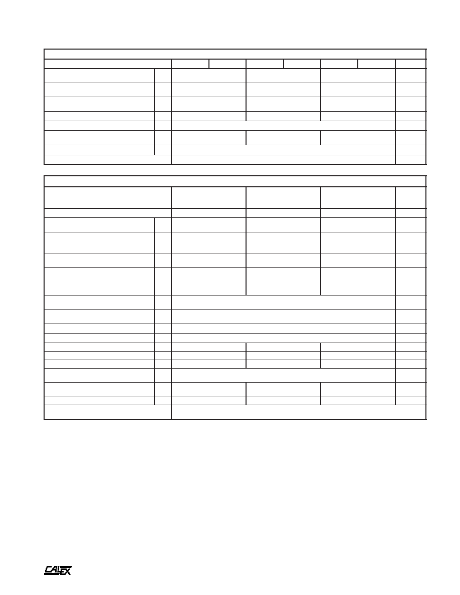
55 Watt K Triple Series DC/DC Converters
Manufacturing Company, Inc. ∑ Concord, California 94520 ∑ Ph: 925/687-4411 or 800/542-3355 ∑ Fax: 925/687-3333 ∑ www.calex.com ∑ Email: sales@calex.com
1
eco# 041007-1
4
5
2
3
6
7
+ INPUT
+ INPUT
- INPUT
- INPUT
ON/OFF
CASE
10 +5V OUTPUT
9 +5 CMN
11
8
14
13
12
+5V SENSE
+5V CMN SENSE
+DUAL OUTPUT
DUAL CMN
-DUAL OUTPUT
DOUBLE SHIELDED
ISOLATION TRANSFORMER
COMMON &
DIFFERENTIAL
MODE INPUT
FILTER
ANTI-PHASE
DUAL PWM
CONTROLLER
SINGLE SECTION
THERMAL SHUTDOWN
ISOLATION
BARRIER
DUAL SECTION
SHIELDED, LOW THERMAL GRADIENT
ALUMINUM CASE
1.5M || 0.01µF
Features
Very Low Noise, < 50 mV P-P Maximum
PCB Mounting with Optional Heat Sink or
Chassis Mount Versions
Efficiencies to 87%
Common and Differential Mode Input Filtering
Remote Sense On +5 Volt Output
Single and Dual Outputs are Isolated From
Each Other
No derating to 80∞C Case Temperature
Five Year Warranty
Description
The 55 Watt Triple Series consists of separate power sections
for the single and dual outputs. These power sections are
operated in anti-phase to each other to reduce the ripple
current stress on the input components and the reflected input
ripple. The main benefit of two separate power sections is the
excellent regulation achieved by all outputs. An order of
magnitude regulation improvement is obtained over
competitive designs. There is no cross regulation between +5
output and the dual outputs. This means that the dual output
voltages are independent of the +5 Volt loading and visa
versa.
Excellent noise performance is attained by using a 0.040
inch thick aluminum case, pot core and toroidal magnetics,
double shielded transformers and both normal mode and
common mode input filtering.
The input and outputs are protected from overvoltage by
transient voltage suppressor diodes. The outputs are protected
from faults with pulse by pulse digital current limiting.
55 Watt Triple Series Block Diagram
t
r
a
h
C
n
o
i
t
c
e
l
e
S
l
e
d
o
M
e
g
n
a
R
t
u
p
n
I
C
D
V
s
t
u
p
t
u
O
C
D
V
s
t
u
p
t
u
O
A
m
n
i
M
x
a
M
K
2
1
.
5
T
2
1
0
.
9
0
.
8
1
2
1
±
,
5
0
5
2
1
±
,
0
0
0
5
K
5
1
.
5
T
2
1
0
.
9
0
.
8
1
5
1
±
,
5
0
0
0
1
±
,
0
0
0
5
K
2
1
.
5
T
4
2
0
.
8
1
0
.
6
3
2
1
±
,
5
0
5
2
1
±
,
0
0
0
5
K
5
1
.
5
T
4
2
0
.
8
1
0
.
6
3
5
1
±
,
5
0
0
0
1
±
,
0
0
0
5
K
2
1
.
5
T
8
4
0
.
6
3
0
.
2
7
2
1
±
,
5
0
5
2
1
±
,
0
0
0
5
K
5
1
.
5
T
8
4
0
.
6
3
0
.
2
7
5
1
±
,
5
0
0
0
1
±
,
0
0
0
5

A
55 Watt K Triple Series DC/DC Converters
Manufacturing Company, Inc. ∑ Concord, California 94520 ∑ Ph: 925/687-4411 or 800/542-3355 ∑ Fax: 925/687-3333 ∑ www.calex.com ∑ Email: sales@calex.com
2
eco# 041007-1
(5)
The remote sense pins must be connected to their respective
output pins for proper output voltage and regulation. The combined
drop on each output line to it's respective remote sense pin must
be less than 0.3 volts or 0.6 volts for both sense lines combined.
(6)
Cross regulation is defined as the change in one output when the
other output is changed from minimum to maximum load.
(7)
Short term stability is specified after a 30 minute warm-up at full
load, constant line, load and ambient conditions.
(8)
Transient response is defined as the time for the output to settle
from a 50 to 75% step load change to a 2% error band (rise time
of step = 2µ Sec).
(9)
Dynamic response is defined as the peak overshoot during a
transient as defined in note 8 above.
(10) The input ripple rejection is specified for DC to 120 Hz ripple with
a modulation amplitude of 1% of Vin.
NOTES
*
All parameters measured at Tc = 25 ∞C, nominal input
voltage and full rated load unless otherwise noted. Refer to
the CALEX Application Notes for the definition of terms,
measurement circuits and other information.
(2)
Noise is measured per CALEX Application Notes. Measurement
bandwidth is 0 - 20 MHz.
(3)
Determine the correct fuse size by calculating the maximum DC
current drain at low line input, maximum load and then adding
20 to 25% to get the desired fuse size. A slow blow type fuse is
recommended. For reverse voltage protection on the input this
fuse must be used.
(4)
Minimum load is required for rated regulation only, no module
damage will occur if the output is run at less than minimum load.
Maximum output power on the dual section is 30 Watts (i.e. one
output can draw 30 Watts and the other 0 Watts). Regulation
degrades with substantial loading unbalance.
*
s
r
e
t
e
m
a
r
a
P
t
u
p
n
I
l
e
d
o
M
K
2
1
.
5
T
2
1
K
5
1
.
5
T
2
1
K
2
1
.
5
T
4
2
K
5
1
.
5
T
4
2
K
2
1
.
5
T
8
3
K
5
1
.
5
T
8
4
s
t
i
n
U
e
g
n
a
R
e
g
a
t
l
o
V
N
I
M
X
A
M
0
.
9
0
.
8
1
0
.
8
1
0
.
6
3
0
.
6
3
0
.
2
7
C
D
V
w
b
z
H
M
0
2
-
0
,
)
2
(
e
l
p
p
i
R
d
e
t
c
e
l
f
e
R
P
Y
T
X
A
M
0
1
1
0
5
2
0
6
0
5
1
5
3
0
8
P
-
P
A
m
d
a
o
L
ll
u
F
t
n
e
r
r
u
C
t
u
p
n
I
d
a
o
L
o
N
P
Y
T
P
Y
T
0
3
6
5
0
5
5
1
7
2
5
3
5
2
3
1
0
3
A
m
y
c
n
e
i
c
i
f
f
E
P
Y
T
1
8
5
8
7
8
%
y
c
n
e
u
q
e
r
F
g
n
i
h
c
t
i
w
S
P
Y
T
0
8
z
H
k
s
m
0
0
1
,
e
g
a
t
l
o
v
r
e
v
O
t
u
p
n
I
m
u
m
i
x
a
M
e
g
a
m
a
D
o
N
X
A
M
3
2
5
4
5
8
C
D
V
r
o
r
r
E
t
u
p
t
u
O
%
1
,
e
m
i
T
n
o
-
n
r
u
T
P
Y
T
0
7
s
m
e
s
u
F
d
e
d
n
e
m
m
o
c
e
R
)
3
(
S
P
M
A
*
s
r
e
t
e
m
a
r
a
P
t
u
p
t
u
O
l
e
d
o
M
K
5
1
.
5
T
2
1
K
2
1
.
5
T
2
1
K
5
1
.
5
T
4
2
K
2
1
.
5
T
4
2
K
5
1
.
5
T
8
4
K
2
1
.
5
T
8
4
K
2
1
.
5
T
4
2
K
2
1
.
5
T
2
1
K
2
1
.
5
T
8
4
K
5
1
.
5
T
4
2
K
5
1
.
5
T
2
1
K
5
1
.
5
T
8
4
s
t
i
n
U
e
g
a
t
l
o
V
t
u
p
t
u
O
5
+
2
1
±
5
1
±
C
D
V
)
4
(
t
n
e
r
r
u
C
d
e
t
a
R
N
I
M
X
A
M
0
5
0
0
0
5
0
1
3
0
5
2
1
0
5
2
0
0
0
1
A
m
e
g
n
a
R
e
g
a
t
l
o
V
)
5
(
d
a
o
L
%
0
0
1
N
I
M
P
Y
T
X
A
M
0
5
9
.
4
0
0
0
.
5
0
5
0
.
5
5
2
9
.
1
1
0
0
0
.
2
1
5
7
0
.
2
1
5
2
9
.
4
1
0
0
0
.
5
1
5
7
0
.
5
1
C
D
V
e
c
n
a
l
a
B
t
u
p
t
u
O
)
d
a
o
L
ll
u
F
,
t
u
p
t
u
O
s
u
n
i
M
o
t
s
u
l
P
(
P
Y
T
X
A
M
A
/
N
5
.
0
7
.
0
5
.
0
7
.
0
%
%
0
0
1
-
%
5
2
n
o
i
t
a
l
u
g
e
R
d
a
o
L
%
0
0
1
-
1
P
Y
T
X
A
M
P
Y
T
X
A
M
2
0
.
0
2
.
0
2
0
.
0
2
.
0
8
.
0
2
.
1
0
.
2
0
.
4
7
.
0
2
.
1
0
.
2
0
.
4
%
)
6
(
n
o
i
t
a
l
u
g
e
R
s
s
o
r
C
P
Y
T
X
A
M
A
/
N
A
/
N
8
.
0
2
.
1
7
.
0
2
.
1
%
n
o
i
t
a
l
u
g
e
R
e
n
i
L
C
D
V
x
a
M
-
n
i
M
=
n
i
V
P
Y
T
X
A
M
2
0
.
0
2
.
0
%
)
7
(
y
t
il
i
b
a
t
S
m
r
e
T
t
r
o
h
S
P
Y
T
2
0
.
0
%
y
t
il
i
b
a
t
S
m
r
e
T
g
n
o
L
P
Y
T
2
.
0
s
r
H
k
/
%
)
8
(
e
s
n
o
p
s
e
R
t
n
e
i
s
n
a
r
T
P
Y
T
0
0
5
0
0
4
0
0
4
s
µ
)
9
(
e
s
n
o
p
s
e
R
c
i
m
a
n
y
D
P
Y
T
0
5
2
0
5
2
0
0
2
k
a
e
p
V
m
)
0
1
(
n
o
i
t
c
e
j
e
R
e
l
p
p
i
R
t
u
p
n
I
P
Y
T
5
2
5
1
5
1
B
d
w
b
z
H
M
0
2
-
0
,
e
s
i
o
N
P
Y
T
X
A
M
5
1
0
5
P
-
P
V
m
t
n
e
i
c
i
f
f
e
o
C
e
r
u
t
a
r
e
p
m
e
T
P
Y
T
X
A
M
0
5
0
0
1
0
5
0
0
2
0
5
0
0
2
C
∞
/
m
p
p
)
1
1
(
p
m
a
l
C
e
g
a
t
l
o
v
r
e
v
O
P
Y
T
8
.
6
5
1
8
1
C
D
V
o
t
n
o
i
t
c
e
t
o
r
P
t
i
u
c
r
i
C
t
r
o
h
S
s
t
u
p
t
u
O
ll
a
r
o
f
n
o
m
m
o
C
d
n
a
g
n
i
t
i
m
il
t
n
e
r
r
u
c
h
t
i
w
n
o
i
t
c
e
t
o
r
p
s
u
o
u
n
i
t
n
o
c
s
r
u
o
h
8
f
o
m
u
m
i
n
i
m
s
e
d
i
v
o
r
P
s
e
u
q
i
n
h
c
e
t
d
a
o
l
r
e
v
o
l
a
m
r
e
h
t

A
55 Watt K Triple Series DC/DC Converters
Manufacturing Company, Inc. ∑ Concord, California 94520 ∑ Ph: 925/687-4411 or 800/542-3355 ∑ Fax: 925/687-3333 ∑ www.calex.com ∑ Email: sales@calex.com
3
eco# 041007-1
Heat Sink Option (-HS suffix)
Chassis Mount Option (-CM suffix)
BOTTOM VIEW
Mounting Configuration Options
To order the optional heat sink on the pin mount version place
a "-HS" suffix on the part number. To order the chassis mount
version place a "-CM" suffix on the part number. The heat sink
and chassis mount options cannot be used together.
(11) For module protection only, see also note 3.
(12) The ON/OFF pin is Open Collector TTL, CMOS, and relay
compatible. The input to this pin is referenced to -Input (pin 2).
(13) The functional temperature range is intended to give an additional
data point for use in evaluating this power supply. At the low
functional temperature the power supply will function with no
side effects, however, sustained operation at the high functional
temperature will reduce expected operational life. The data
sheet specifications are not guaranteed over the functional
temperature range.
(14) The case thermal impedance is specified as the case temperature
rise over ambient per package watt dissipated. The thermal
resistance of the Chassis Mount version depends on the mounting
surface. If the mounting surface is a poor thermal conductor the
thermal resistance can be as high as 2.7∞ C/watt. If the mounting
surface is an excellent thermal conductor the thermal resistance
can be below 1∞C/watt.
(15) Water Washability - Calex DC/DC converters are designed to
withstand most solder/wash processes. Careful attention should
be used when assessing the applicability in your specific
manufacturing process. Converters are not hermetically sealed.
Mechanical tolerances unless otherwise noted:
X.XX dimensions: ±0.020 inches
X.XXX dimensions: ±0.005 inches
Seal around terminals is not hermetic. Do not immerse units in any
liquid.
*
s
n
o
i
t
a
c
i
f
i
c
e
p
S
l
a
r
e
n
e
G
s
l
e
d
o
M
l
l
A
s
t
i
n
U
)
2
1
(
n
o
i
t
c
n
u
F
F
F
O
/
N
O
l
e
v
e
L
c
i
g
o
L
N
O
n
e
p
O
n
i
P
e
v
a
e
L
r
o
N
I
M
5
.
4
C
D
V
l
e
v
e
L
c
i
g
o
L
F
F
O
X
A
M
2
.
1
C
D
V
e
c
n
a
t
s
i
s
e
R
t
u
p
n
I
P
Y
T
2
s
m
h
o
k
,
t
n
e
r
r
u
C
e
l
d
I
r
e
t
r
e
v
n
o
C
w
o
L
n
i
P
F
F
O
/
N
O
P
Y
T
5
2
A
m
n
o
i
t
a
l
o
s
I
e
g
a
t
l
o
V
n
o
i
t
a
l
o
s
I
t
u
p
t
u
O
r
e
h
t
i
E
o
t
t
u
p
n
I
t
u
p
t
u
O
l
a
u
D
o
t
e
l
g
n
i
S
e
s
a
C
-
t
u
p
n
I
e
s
a
C
o
t
t
u
p
t
u
O
r
e
h
t
i
E
e
g
a
k
a
e
L
A
µ
0
1
N
I
M
N
I
M
N
I
M
N
I
M
4
4
5
1
0
0
7
0
5
2
4
4
5
1
C
D
V
e
c
n
a
t
i
c
a
p
a
C
t
u
p
t
u
O
o
t
t
u
p
n
I
t
u
p
t
u
O
e
l
g
n
i
S
o
t
t
u
p
n
I
t
u
p
t
u
O
l
a
u
D
o
t
t
u
p
n
I
t
u
p
t
u
O
l
a
u
D
o
t
e
l
g
n
i
S
P
Y
T
P
Y
T
P
Y
T
0
0
1
0
5
1
5
7
F
p
l
a
t
n
e
m
n
o
r
i
v
n
E
e
g
n
a
R
g
n
i
t
a
r
e
p
O
e
s
a
C
g
n
i
t
a
r
e
D
o
N
N
I
M
X
A
M
5
2
-
0
8
C
∞
)
3
1
(
e
g
n
a
R
l
a
n
o
i
t
n
u
F
e
s
a
C
N
I
M
X
A
M
0
4
-
0
9
C
∞
e
g
n
a
R
e
g
a
r
o
t
S
N
I
M
X
A
M
0
4
-
0
0
1
C
∞
)
4
1
(
e
c
n
a
d
e
p
m
I
l
a
m
r
e
h
T
n
o
i
s
r
e
V
t
n
u
o
M
n
i
P
)
k
n
i
S
t
a
e
H
(
S
H
-
n
o
i
t
p
O
s
i
s
s
a
h
C
(
M
C
-
n
o
i
t
p
O
)
t
n
u
o
M
P
Y
T
P
Y
T
7
.
2
8
.
1
)
4
1
(
t
t
a
W
/
C
∞
n
w
o
d
t
u
h
S
l
a
m
r
e
h
T
e
r
u
t
a
r
e
p
m
e
T
e
s
a
C
P
Y
T
0
9
C
∞
l
a
r
e
n
e
G
t
h
g
i
e
W
t
i
n
U
4
1
.
z
o
s
t
i
K
g
n
i
t
n
u
o
M
s
n
o
i
t
p
O
e
s
a
C
e
e
S
n
i
P
n
o
i
t
c
n
u
F
n
i
P
n
o
i
t
c
n
u
F
1
N
I
P
O
N
8
E
S
N
E
S
N
M
C
V
5
+
2
T
U
P
N
I
-
9
N
M
C
V
5
+
3
T
U
P
N
I
-
0
1
T
U
P
T
U
O
V
5
+
4
T
U
P
N
I
+
1
1
E
S
N
E
S
V
5
+
5
T
U
P
N
I
+
2
1
T
U
P
T
U
O
L
A
U
D
-
6
F
F
O
/
N
O
3
1
N
M
C
L
A
U
D
7
E
S
A
C
4
1
T
U
P
T
U
O
L
A
U
D
+

A
55 Watt K Triple Series DC/DC Converters
Manufacturing Company, Inc. ∑ Concord, California 94520 ∑ Ph: 925/687-4411 or 800/542-3355 ∑ Fax: 925/687-3333 ∑ www.calex.com ∑ Email: sales@calex.com
4
eco# 041007-1
Dual Output
The dual outputs are cross regulated to each other but
independent of the loading on the single output. The dual
output uses a cross regulation scheme where the plus and
minus output voltage is regulated as an average voltage. This
allows improved regulation on both outputs. If the outputs are
loaded equally and the regulation is checked, then the apparent
regulation is much closer to 0.5%. This data shows the worst
case result of changing each output independently. The
output common on the dual section is electrically isolated from
the +5 volt section to aid in proper system grounding. If 24
volts or 30 volts are required, then the appropriate output can
be connected to the system ground and the output current can
be taken from the other output. In this situation the dual
section's common pin (Pin 13) should be left unconnected.
Full output power (30 watts) is available in this configuration.
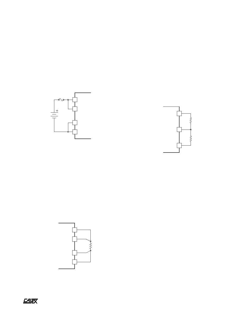
Figure 3 shows the dual output connections.
Figure 3.
The dual outputs can also be used with substantial unbalance and
as single-ended outputs by leaving Pin 13 unconnected.
Mounting Guidelines
The 55 Watt Triple Series can be supplied in either a pin mount
version or a chassis mount (screw terminal) version. It is
suggested that when using the pin mount version, the 4-40
hold down screws provided in the bottom of the case be used
to secure the unit to the PCB. These screws should be
tightened before soldering to avoid solder joint stress.
The chassis mount version can be mounted on its back
with the four 4-40 hold down screws provided. The mounting
surface should be flat to within 0.01 inches to prevent warping
the case. The mounting can then serve as additional heat
sinking. For optimum heat sinking, silicone grease is
recommended over the so called "dry pads." Additional heat
sinking will lower internal temperatures and increase the
expected life. When chassis mounting remember that the
case is connected to the - INPUT pins through 1.5 Megohms
in parallel with 0.01µF. The breakthrough voltage of this
connection is greater than 250VDC.
The "-HS" heat sink option lowers the thermal resistance
from 2.7 to 1.8∞C/Watt dissipated. It also increases the heat
removing efficiency of any cooling air flow. If the 55 Watt Triple
is to be placed in a small enclosure where the power delivered
to the load or the power dissipated in the 55 Watt Triple
converter can raise the ambient temperature then care must
be taken to insure that the case temperature does not exceed
the 80∞C limit for proper operation.
14
13
12
+LOAD
-LOAD
+DUAL OUTPUT
DUAL CMN
-DUAL OUTPUT
10
11
8
9
+5V OUTPUT
+5V SENSE
+5V CMN SENSE
+5V CMN
LOAD
4
5
2
3
FUSE
SOURCE
+INPUT
-INPUT
Application Guidelines
Inputs
The input should be fused as per note number 3. The case is
connected to the -INPUT pins through 1.5 Megohms in
parallel with 0.01µF. The case may be left floating in most
applications. The noise performance of the converter may
improve or degrade with the case connected to other inputs or
outputs depending on your system grounding.
The remote ON/OFF pin may be left floating if it is not used.
See "Understanding the Remote ON/OFF Function" application
note for more information on this feature.
The dual input pins (2,3 and 4,5) should be paralleled to
share the input current. Figure 1 shows the recommended
input connections.
Figure 1.
Parallel both + and -INPUT pins. Fusing the input is recommended.
Single Output
The single output is independent of the loading on the dual
output section. The single output also features provisions for
remote sense connections. These allow the power supply to
correct for line drops of up to 0.3 volts per leg or 0.6 volts total.
The remote sense connections should be made with twisted
pair wire or closely coupled PCB traces. There is approximately
2mA of current flowing in the remote sense lines. If the remote
sense is not to be used, these pins must be connected to their
respective output pins for proper output voltage accuracy and
regulation. See "Applying the Remote Sense and Trim
Functions On DC/DC Converters" application note for more
information. The output common on the single section is
electrically isolated from the dual section to aid in proper
system grounding. Figure 2 shows the single output
connections with remote sense.
Figure 2.
The remote sense pins must be connected to their respective
outputs. If the remote sense feature is not used, connect the sense
pins to their outputs directly at the converter.

A
55 Watt K Triple Series DC/DC Converters
Manufacturing Company, Inc. ∑ Concord, California 94520 ∑ Ph: 925/687-4411 or 800/542-3355 ∑ Fax: 925/687-3333 ∑ www.calex.com ∑ Email: sales@calex.com
5
eco# 041007-1
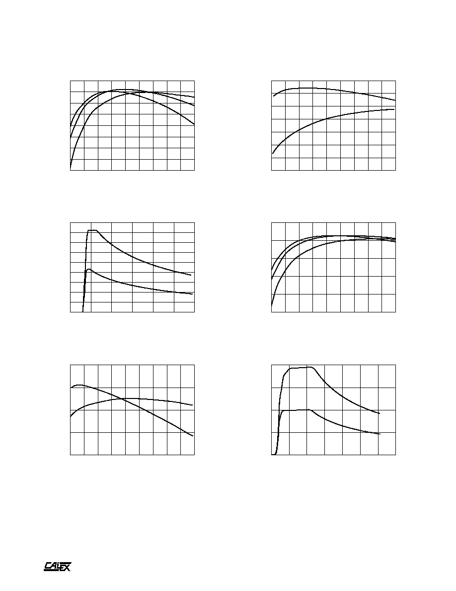
Typical Performance (Tc=25∞C, Vin=48 VDC, Rated Load).
10
20
30
40
50
60
70
80
90
100
LOAD (%)
70
72
74
76
78
80
82
84
86
EFFICIENCY (%)
12T5.XXK EFFICIENCY Vs. LOAD
LINE =
LINE =
LINE =
12VDC
9VDC
18VDC
9
10
11
12
13
14
15
16
17
18
LINE INPUT (VOLTS)
78
79
80
81
82
83
84
85
EFFICIENCY (%)
12T5.XXK EFFICIENCY Vs. LINE INPUT
50% FULL LOAD
100% FULL LOAD
6
8
10
12
14
16
18
LINE INPUT (VOLTS)
0
1
2
3
4
5
6
7
8
9
INPUT CURRENT (AMPS)
12T5.XXK INPUT CURRENT Vs. LINE INPUT VOLTAGE
100% FULL LOAD
50% FULL LOAD
10
20
30
40
50
60
70
80
90
100
LOAD (%)
65
70
75
80
85
90
EFFICIENCY (%)
24T5.XXK EFFICIENCY Vs. LOAD
LINE = 18VDC
LINE =
LINE = 36VDC
24VDC
18
20
22
24
26
28
30
32
34
36
LINE INPUT (VOLTS)
83
84
85
86
87
EFFICIENCY (%)
24T5.XXK EFFICIENCY Vs. LINE INPUT
50% FULL LOAD
100% FULL LOAD
5
10
15
20
25
30
35
40
LINE INPUT (VOLTS)
0.0
1.0
2.0
3.0
4.0
INPUT CURRENT (AMPS)
24T5.XXK INPUT CURRENT Vs. LINE INPUT VOLTAGE
100% FULL LOAD
50% FULL LOAD

