 | –≠–ª–µ–∫—Ç—Ä–æ–Ω–Ω—ã–π –∫–æ–º–ø–æ–Ω–µ–Ω—Ç: 4902-230 | –°–∫–∞—á–∞—Ç—å:  PDF PDF  ZIP ZIP |
A
2401 Stanwell Drive ∑ Concord, California 94520 ∑ Ph: 925/687-4411 or 800/542-3355 ∑ Fax: 925/687-3333 ∑ www.calex.com ∑ Email: sales@calex.com
1
4/2001
Model 176 and 178 DC Amplifiers
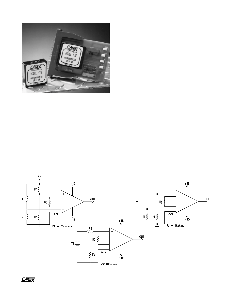
FIGURE 1. Basic Bridge Amplifier
FIGURE 3. Thermocouple Amplifier
FIGURE 2. High Source Impedance Amplifier
Features*
!
Drifts to <0.25µV/∞C
!
Input Impedance >100 M
!
CMR: 120 dB @ G = 1000
!
Gain Linearity of ±.005%
*The key features of this amplifier series, listed above, do not
necessarily apply to all units. Please check individual unit
specifications.
Description
The 176 (all versions) and the 178 are general purpose
differential input DC amplifiers. The best all-around unit is the
178. It features premium performance over a gain range of 1
to 1,000. With adjustable CMR, gain, and input and output
offsets it truly approaches the ideal instrumentation amplifier.
Applications
Below are three typical applications showing the versatility of
this instrumentation amplifier series.
Figure 1 shows the basic connections for a bridge amplifier.
The bridge can be a transducer, strain gage or a load cell. The
amplifier rejects the common mode voltage and noise of the
bridge and only amplifies the difference between the + and -
inputs. In most cases the bridge impedance is less than 1 k
which would make the 176 ideal.
Figure 2 shows a single ended application where the input
signal has a high source impedance. Since the 178 has
extremely high input impedance and low bias current, it would
be the choice. Better balance and drift can be achieved by
matching the source impedance with a resistor of equal value
from the - input to common.
Figure 3 shows a thermocouple amplifier. By utilizing the two
resistors on the inputs, the high common mode rejection of the
amplifiers can be used to remove 60 Hz noise on the lines or
external voltage floating on the input lines. The thermocouples
can float to ±10 Volts. Since thermocouples are low impedance
devices, the 176 is recommended.
Note: With either the 176 or 178 Amplifier it is required that the
source common be electrically tied to signal common and the
power source common. Both amplifiers are bipolar direct
coupled and require a return path for the input signal current
for stable operation.

A
2401 Stanwell Drive ∑ Concord, California 94520 ∑ Ph: 925/687-4411 or 800/542-3355 ∑ Fax: 925/687-3333 ∑ www.calex.com ∑ Email: sales@calex.com
2
4/2001
Model 176 and 178 DC Amplifiers
Specifications
Typical @ 25∞C and ±15 VDC unless noted
176 ONLY
178 ONLY
Mechanical Specifications
Dimensions given in inches.
FIGURE 5.
FIGURE 4.
l
e
d
o
M
J
6
7
1
K
6
7
1
L
6
7
1
8
7
1
n
i
a
G
e
g
n
a
R
0
0
0
1
o
t
0
1
0
0
0
1
o
t
1
a
l
u
m
r
o
F
n
i
a
G
R
/
m
h
o
l
i
k
0
0
2
+
0
1
g
R
/
m
h
o
l
i
k
0
2
+
1
g
y
c
a
r
u
c
c
A
a
l
u
m
r
o
F
n
i
a
G
%
2
±
%
2
.
0
±
%
2
.
0
±
%
2
.
0
±
.
x
a
m
,
y
t
i
r
a
e
n
i
L
n
i
a
G
%
5
0
0
.
0
±
t
n
e
i
c
i
f
f
e
o
C
e
r
u
t
a
r
e
p
m
e
T
n
i
a
G
/
m
p
p
0
2
∞
.
x
a
m
C
t
u
p
n
I
.
f
f
i
D
-
e
c
n
a
d
e
p
m
I
t
u
p
n
I
M
0
1
M
0
0
0
1
M
C
-
e
c
n
a
d
e
p
m
I
t
u
p
n
I
M
0
0
5
M
0
0
0
1
M
C
-
e
g
n
a
R
e
g
a
t
l
o
V
t
u
p
n
I
V
0
1
±
V
6
±
V
0
1
±
)
R
M
C
(
n
o
i
t
c
e
j
e
R
e
d
o
M
n
o
m
m
o
C
0
0
1
=
n
i
a
G
,
z
H
0
6
o
t
C
D
B
d
0
0
1
)
t
u
p
n
I
o
t
d
e
r
r
e
f
e
R
(
s
t
e
s
f
f
O
t
u
p
n
I
)
I
T
R
(
e
g
a
t
l
o
V
s
t
e
s
f
f
O
l
a
i
t
i
n
I
)
o
r
e
z
o
t
.
j
d
A
(
0
0
0
1
=
G
C
∞
5
2
@
V
µ
0
0
3
±
V
µ
0
0
1
±
V
µ
0
5
±
V
µ
0
0
3
±
.
x
a
m
,
e
r
u
t
a
r
e
p
m
e
T
.
s
V
0
1
=
G
0
0
0
1
=
G
/
V
µ
0
1
±
∞C
/
V
µ
3
±
∞C
/
V
µ
5
±
∞C
/
V
µ
1
±
∞C
/
V
µ
3
±
∞C
/
V
µ
5
2
.
0
±
∞C
/
V
µ
3
±
∞C
/
V
µ
2
±
∞C
.
x
a
m
,
y
l
p
p
u
S
.
s
V
V
/
V
µ
0
5
.
x
a
m
,
C
∞
5
2
@
t
n
e
r
r
u
C
s
a
i
B
t
u
p
n
I
A
n
0
5
±
A
n
0
4
±
A
n
0
5
2
±
A
n
0
1
±
t
n
e
r
r
u
C
e
c
n
e
r
e
f
f
i
D
t
u
p
n
I
.
x
a
m
,
e
r
u
t
a
r
e
p
m
e
T
.
s
V
/
A
n
2
.
0
±
∞C
/
A
n
5
0
.
0
±
∞C
/
A
n
1
.
0
±
∞C
/
A
n
3
0
.
0
±
∞C
R
(
e
s
i
o
N
t
u
p
n
I
S
)
m
h
o
k
1
=
z
H
0
1
o
t
z
H
1
.
0
,
)
I
T
R
(
e
s
i
o
N
e
g
a
t
l
o
V
0
0
0
1
=
G
S
M
R
V
µ
5
0
.
0
S
M
R
V
µ
1
0
.
0
z
H
k
0
1
o
t
z
H
0
1
,
)
I
T
R
(
e
s
i
o
N
e
g
a
t
l
o
V
0
0
0
1
=
G
S
M
R
V
µ
5
S
M
R
V
µ
1
t
u
p
t
u
O
t
u
p
t
u
O
d
e
t
a
R
.
n
i
m
,
e
g
a
t
l
o
V
.
n
i
m
,
t
n
e
r
r
u
C
V
0
1
±
A
m
5
±
z
H
k
1
o
t
C
D
,
e
c
n
a
d
e
p
m
I
t
u
p
t
u
O
m
h
o
1
e
s
n
o
p
s
e
R
y
c
n
e
u
q
e
r
F
E
(
e
s
n
o
p
s
e
R
l
a
n
g
i
S
ll
a
m
S
n
i
)
S
M
R
V
m
0
1
=
r
o
f
0
0
1
=
G
t
a
±
y
c
a
r
u
c
c
A
n
i
a
G
%
1
n
w
o
d
B
d
3
,
0
0
1
=
G
t
a
.
n
i
m
z
H
k
1
z
H
k
0
1
.
n
i
m
z
H
0
0
5
z
H
k
5
e
t
a
R
w
e
l
S
s
µ
/
V
5
.
0
s
µ
/
V
1
.
0
e
g
n
a
R
y
l
p
p
u
S
r
e
w
o
P
s
c
e
p
S
d
e
t
a
R
,
e
g
a
t
l
o
V
y
l
p
p
u
S
V
6
1
±
o
t
V
4
1
±
n
i
a
r
D
t
n
e
r
r
u
C
t
n
e
c
s
e
i
u
Q
A
m
5
.
3
±
A
m
3
1
±
e
g
n
a
R
e
r
u
t
a
r
e
p
m
e
T
g
n
i
t
a
r
e
p
O
5
2
-
∞
1
7
+
o
t
C
∞C
A
2401 Stanwell Drive ∑ Concord, California 94520 ∑ Ph: 925/687-4411 or 800/542-3355 ∑ Fax: 925/687-3333 ∑ www.calex.com ∑ Email: sales@calex.com
3
4/2001
Model 176 and 178 DC Amplifiers
Operation and Adjustment
Figure 10 shows pin connections for the Model 176 when
used with external offset trim. Offset is quite low on the
untrimmed unit and external trimming is normally not needed.
If external trimming is used and ambient temperature varies
widely, a potentiometer and resistor with good temperature
coefficient should be used. Range of adjustment is ±3 mV
referred to the input. Gain is adjusted by means of R
g
which
should be a low power, temperature stable, precision resistor.
The wire leads to R
g
should be kept as short as possible to
avoid noise pickup. If it is necessary to locate R
g
some
distance from the amplifier, a shielded twisted pair should be
used for the connection.
There must be a current path from the amplifier inputs to
power supply common to allow the input bias current to flow.
A floating signal source can generally be accommodated by
connecting a 1 M
resistor between input signal ground and
the amplifier common. This provides a return path for the
amplifier input bias current.
FIGURE 8.
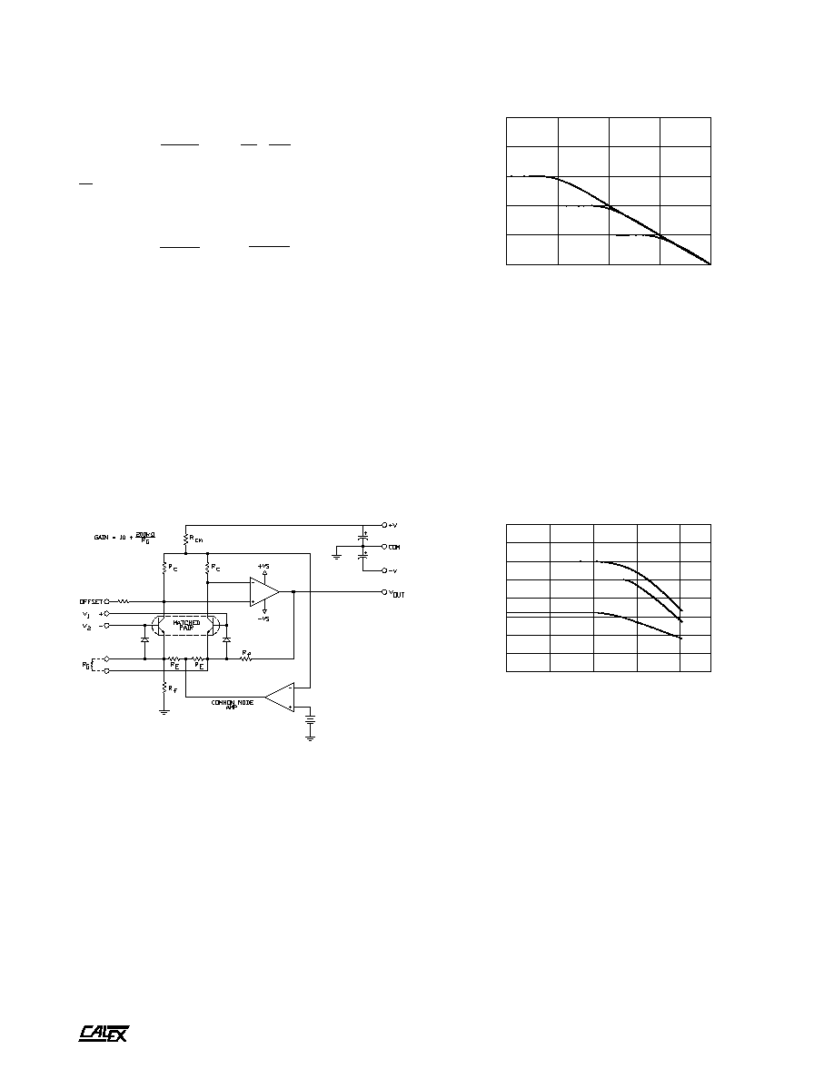
Common Mode Rejection (CMR)
The Model 176 provides excellent CMR at DC and higher
frequencies. One of the frequencies of interest is 60 Hz and
it can be seen from Figure 8 that the CMR is virtually unchanged
from DC to 60 Hz. Higher frequencies are important also and
the Model 176 maintains good CMR to over 1 kHz. For
example, it may be desired to operate a bridge circuit with an
AC voltage source such as 400 Hz. The Model 176 can still
function as a differential bridge amplifier with a CMR of almost
100 dB (G = 100) at that frequency.
FIGURE 7.
100
1000
10000
100000
1000000
FREQUENCY - Hz
0
20
40
60
80
100
GAIN - db
TYPICAL SMALL SIGNAL FREQUENCY RESPONSE
G = 10
G = 100
G = 1000
5000
.1
1
10
100
1000
FREQUENCY (Hz)
60
70
80
90
100
110
120
130
140
COMMON MODE REJECTION - db
CMR Vs. FREQUENCY
G = 1000
G = 100
G = 10
Theory of Operation
In Figure 6, the amplifier differential gain is:
V
out
=
1 +
R
f
+
2 R
f
V
1
- V
2
R
E
R
g
R
f
is chosen to be precisely 9 ±0.05%
R
E
Since R
f
is equal to 100 k
, this results in a gain equation of
V
out
=
10 +
200 k
V
1
- V
2
R
g
The accuracy of this equation depends on careful matching of
the various resistors and the quality of the transistor input pair.
The Model 176 uses a special input pair that is designed
especially for high performance instrument amplifiers. Diodes
between base and emitter provide input protection of up to
±20 Volts differential or common mode.
To provide the ultimate in CMR, a separate operational
amplifier is used to feedback common-mode voltage to the
input pair. A Common-mode voltage is generated across R
cm
which is then fed into the common-mode amplifier input. This
amplifier also serves as a current source for the input differential
pair. Since some gain is provided by the input transistor, the
op amp is operated at lower closed loop gains allowing gain
linearity and bandwidth to be significantly better than when all
gain is provided by a single op amp.
FIGURE 6. Simplified Schematic of Model 176
Frequency Response
Bode plots of the Model 176 gain for gains of 10,100 and 1000
are shown in Figure 7. The frequency response has been
designed to equal a single pole roll-off with a damping ratio of
approximately 0.7. This prevents a ringing response if the
amplifier is used with square wave or pulse input signals. Gain
error is less than ±1% and phase shift is less than 6∞ at
frequencies lower than 1 /10 of the 3 dB down frequency for
any gain. If gain accuracy of better than ±0.1 % is desired, gain
magnitude should be adjusted so that the highest signal
frequency to be amplified is less than 0.05 times the 3 dB
down frequency.
A
2401 Stanwell Drive ∑ Concord, California 94520 ∑ Ph: 925/687-4411 or 800/542-3355 ∑ Fax: 925/687-3333 ∑ www.calex.com ∑ Email: sales@calex.com
4
4/2001
Model 176 and 178 DC Amplifiers
Description
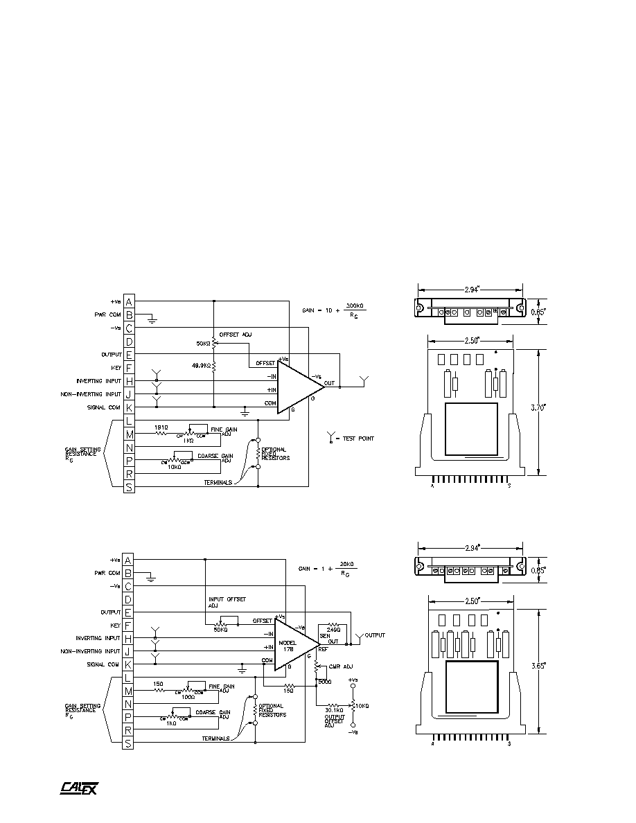
Connections to the Model 178 are made as shown on the
mounting kit (Figure 11). The gain setting impedance can be
a fixed resistor or can be a potentiometer when variable gain
is needed. Input offset is adjusted by means of the 50 kohm
potentiometer between +15V and trim. If needed, common-
mode-rejection can be externally trimmed by connecting a
249
resistor between sense and out and a 500
potentiometer between ref (pin 10) and com. The MK278
mounting kit has provisions for adjusting offset and CMR on
the PC card.
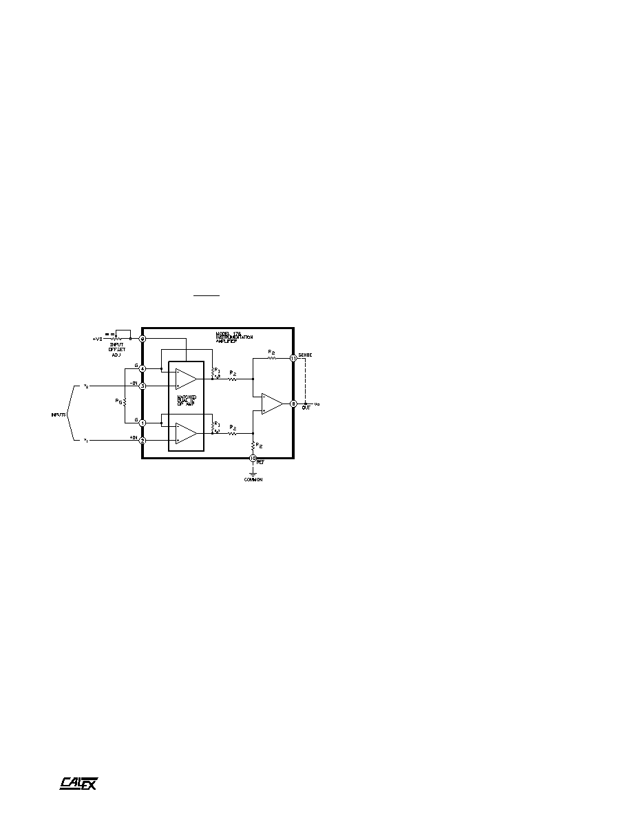
Theory of Operation
The Model 178 is a committed gain amplifier with high input
impedance looking into either input. A simplified block diagram
is shown in Figure 9. The input stage is a matched dual IC op
amp that is manufactured to CALEX specifications. The tight
matching of the two high performance input amplifiers and
their close physical proximity ensures excellent temperature
tracking and very good rejection of common mode inputs.
The output stage is a low-drift, low-noise IC op amp. Remote
sense and output reference terminals are provided at the
output stage. In most applications, the sense terminal is
simply connected to the amplifier output and the REF terminal
is connected to the system common as shown in Figure 9; but
these terminals can be used to externally trim CMR or to
develop current amplifier configurations. In addition, an output
offset can be applied to the amplifier by putting an offset
voltage on the REF terminal.
The overall gain equation is:
GAIN =1 +
20 k
R
g
Input Offset Adjustment
With gain set at any desired level above 10, connect both input
leads (pins 2 and 3) to signal common (pin 6). Adjust the input
offset adj pot for zero at the amplifier output. Offset at low
gains is primarily due to offset of the output amplifier and will
be less than +1 mV. If the amplifier gain is to be varied over a
wide range, it is best to adjust input offset at the maximum gain
to be used. The MK278 mounting kit has provisions for
adjusting both offsets. With the amplifier connected for unity
gain (open circuit between pins L and S on the connector) and
the inputs connected to common, vary the output offset adj pot
for zero at the amplifier output. Then connect the amplifier for
the maximum gain of interest and adjust the offset by varying
the input offset adj. Repeat both adjustments if necessary.
Output Offset
Offset of the output stage can be directly varied over a wide
range by disconnecting the ref input pin (pin 10) from common
and applying a voltage to the ref input. The output level can be
adjusted over a range of +10V independent of initial offset
adjustments. Source impedance of the offsetting voltage
must be very low in order to not degrade CMR. The impedance
at pin 10 is approximately 160 k
. For best results, the
offsetting voltage should be supplied through an operational
amplifier with low output impedance.
Gain Adjustment
The gain can be set by fixed resistors or a gain pot. Gain of the
Model 178 is deliberately trimmed to be low by 3% to 5% for
infinite RG, thus assuring that the amplifier can be set for unity
gain. This is valid even with the external CMR adjustment
circuit as shown in Figure 11. This makes the gain range
somewhat greater than the nominal range of 1 to 1000. Above
100, gain is primarily determined by the 20 k
/R
G
term, which
is accurate to within ±0.2%. For Gain = 1, R
G
will be 400 K to
1 megohm.
Common Mode Rejection
The key advantage of using a differential input instrumentation
amplifier is its ability to reject common-mode inputs. The
common-mode input generally consists of a DC component
plus 60 Hz noise. To externally adjust CMR, connect the two
inputs together (pins 2 and 3) and apply a low frequency ±10V
sine wave. The gain should be set to the lowest value that will
be used, then vary the CMR ADJ pot for minimum amplifier
output. The CMR is 20 log
10
(A
d
/A
cm
), where A
d
is the differential
gain setting and A
cm
is the undesired common-mode gain. The
Model 178 can be readily trimmed to CMR of better than 120
dB at DC.
FIGURE 9. Simplified Circuit Diagram for Model 178
A
2401 Stanwell Drive ∑ Concord, California 94520 ∑ Ph: 925/687-4411 or 800/542-3355 ∑ Fax: 925/687-3333 ∑ www.calex.com ∑ Email: sales@calex.com
5
4/2001
Model 176 and 178 DC Amplifiers
MODEL
176
Mounting Kits
Operation with Mounting Kit
When the Model 176 is mounted on a Model MK276 Mounting
Kit, all necessary gain setting and offset adjustments are
provided. A schematic and outline are shown in Figure 10.
Gain can be set in several different ways. For committed gain
applications, a fixed resistor may be soldered to the two
terminals on the PC board. By jumpering pin L to M and pin S
to N, gain may be adjusted from approximately 200 to 1000
with the fine gain adjust trimpot. By jumpering L to M, N to P
and R to S, the gain may be adjusted with the fine and coarse
adjust trimpots with a total gain range of about 30 to 1000. The
low gain range from 10 to 30 is best accommodated by
connecting a fixed resistor (10 kohms to 50 kohms) or external
pot in series with the coarse gain pot.
For convenience during system checkout or troubleshooting,
four testpoints are provided on the PC board which give
access to both terminals and the amplifier output. They are
located at the end of the board so that voltmeter or scope
probes may be inserted even if a number of cards are stacked
in a row.
The MK278 mounting kit has both fine and coarse gain
adjustment pot. The fine gain adjustment pot can be used
alone or for high gains (170 to 1000). Just connect pin L to pin
M and pin N to pin S on the mounting kit. For mid-range gains
(10 to 190), connect both pots in series between pins L and S.
The low gain range is best accommodated by connecting a
fixed resistor or external pot in series with the coarse gain pot.
Also, the mounting kit has terminals on the PC board for
connecting a fixed resistor. If necessary, the gain setting
resistance may be located off the PC board, but this may
degrade frequency response and increase the noise level.
The output offset adjustment has a range of ±7.5 mV.
FIGURE 10. MK276 Electrical Schematic and Mechanical Outline
FIGURE 11. MK278 Electrical Schematic and Mechanical Outline
Model 178/MK278
Model 176/MK276