 | –≠–ª–µ–∫—Ç—Ä–æ–Ω–Ω—ã–π –∫–æ–º–ø–æ–Ω–µ–Ω—Ç: CM1205 | –°–∫–∞—á–∞—Ç—å:  PDF PDF  ZIP ZIP |
© 2003 California Micro Devices Corp. All rights reserved.
11/17/03
430 N. McCarthy Blvd., Milpitas, CA 95035-5112
L Tel: 408.263.3214
L Fax: 408.263.7846 L www.calmicro.com
1
CM1205
ESD Protection Arrays, Chip Scale Package
Features
∑
Functionally and pin compatible with CAMD's
PACDN1404C, PACDN1408C and PACDN1416C
family of ESD protection devices
∑
4, 8, or 16 transient voltage suppressors in a single
package
∑
Optiguard
TM
coated for improved reliability at
assembly
∑
In-system Electrostatic Discharge (ESD) protection
to +25kV contact discharge per IEC 61000-4-2
international standard
∑
Compact Chip Scale Package (0.65mm pitch) for-
mat saves board space and eases layout in space
critical applications compared to discrete solutions
and traditional wire bonded packages
∑
Lead-free versions available
Applications
∑
ESD protection for sensitive electronic equipment
∑
I/O port, keypad and button circuitry protection for
portable devices
∑
Wireless Handsets
∑
Handheld PCs / PDAs
∑
MP3 Players
∑
Digital Cameras and Camcorders
∑
Notebooks
∑
Desktop PCs
Product Description
The CM1205 family of transient voltage suppressor
arrays provides a very high level of protection for sensi-
tive electronic components that may be subjected to
ESD.
These devices are designed and characterized to
safely dissipate ESD strikes at levels well beyond the
maximum requirements set forth in the IEC 61000-4-2
international standard (Level 4, +8kV contact dis-
charge). All I/Os are rated at +25kV using the IEC
61000-4-2 contact discharge method. Using the MIL-
STD-883D (Method 3015) specification for Human
Body Model (HBM) ESD, all pins are protected for con-
tact discharges to greater than +30kV.
The Chip Scale Package format of these devices
enable extremely small footprints that are necessary in
portable electronics such as cellular phones, PDAs,
internet appliances and PCs. The large solder bumps
allow for standard attachment to laminate boards with-
out the use of underfill.
The CM1205 features OptiGuard
TM
coating for
improved reliability at assembly and is available with
optional lead-free finishing.
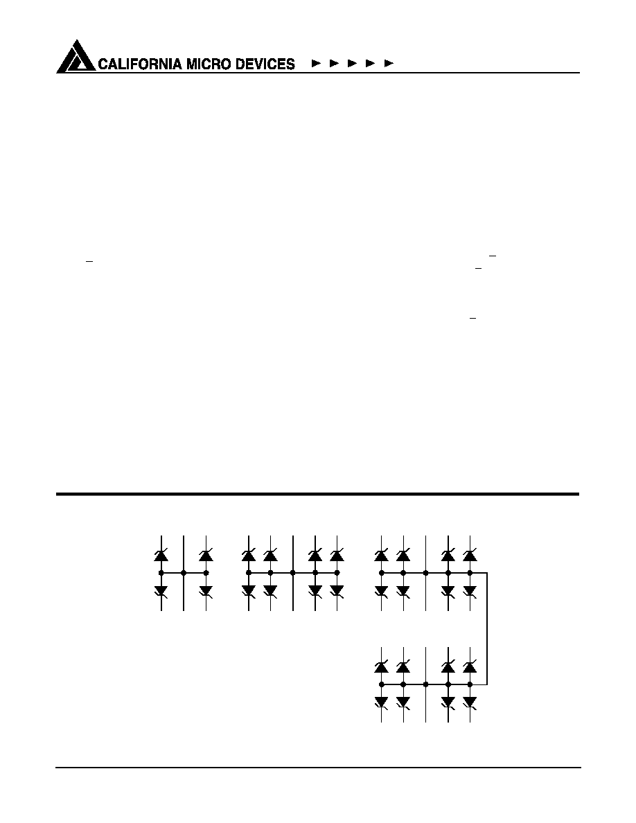
Electrical Schematic
CM1205-04CS/CP
CM1205-08CS/CP
CM1205-16CS/CP
A1
A2
A3
B1
B2
B3
C2
C3
C4
D2
D3
D4
C5
D5
C1
D1
A2
A3
A4
B2
B3
B4
A5
B5
A1
B1
A2
A3
A4
B2
B3
B4
A5
B5
A1
B1
© 2003 California Micro Devices Corp. All rights reserved.
2
430 N. McCarthy Blvd., Milpitas, CA 95035-5112
L Tel: 408.263.3214
L Fax: 408.263.7846 L www.calmicro.com
11/17/03
CM1205
Ordering Information
Note 1: Parts are shipped in Tape & Reel form unless otherwise specified.
Note 2: Lead-free devices are specified by using a "
+
" character for the top side orientation mark.
120516
3
2
5
4
1
B
A
D
C
Orientation
Marking
(see note 2)
120508
3
2
5
4
1
B
A
Orientation
Marking
(see note 2)
L05
3
2
1
B
A
Orientation
Marking
(see note 2)
C3
D3
C2
C1
D2
D1
C5
D5
C4
D4
A3
B3
A2
A1
B2
B1
A5
B5
A4
B4
A3
B3
A2
A1
B2
B1
A5
B5
A4
B4
A3
B3
A2
A1
B2
B1
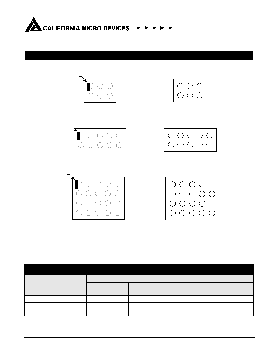
CM1405-04
CSP Package
PACKAGE / PINOUT DIAGRAMS
Notes:
BOTTOM VIEW
(Bumps Up View)
TOP VIEW
(Bumps Down View)
CM1405-08
CSP Package
BOTTOM VIEW
(Bumps Up View)
TOP VIEW
(Bumps Down View)
CSP Package
CM1405-16
BOTTOM VIEW
(Bumps Up View)
TOP VIEW
(Bumps Down View)
1) These drawings are not to scale.
2) Lead-free devices are specified by using a "+" character for the top side orientation mark.
PART NUMBERING INFORMATION
Bumps
Package
Standard Finish
Lead-free Finish
2
Ordering Part
Number
1
Part Marking
Ordering Part
Number
1
Part Marking
6
CSP
CM1205-04CS
L05
CM1205-04CP
L05
10
CSP
CM1205-08CS
120508
CM1205-08CP
120508
20
CSP
CM1205-16CS
120516
CM1205-16CP
120516
© 2003 California Micro Devices Corp. All rights reserved.
11/17/03
430 N. McCarthy Blvd., Milpitas, CA 95035-5112
L Tel: 408.263.3214
L Fax: 408.263.7846
L www.calmicro.com
3
CM1205
Specifications
Note 1: T
A
=25
∞
C unless otherwise specified. GND in this document refers to the lower supply voltage.
Note 2: ESD applied to channel pins with respect to GND, one at a time. All other channels are open. All GND pins tied to ground.
Note 3: These parameters are guaranteed by design and characterization.
ABSOLUTE MAXIMUM RATINGS
PARAMETER
RATING
UNITS
Storage Temperature Range
-65 to +150
∞C
STANDARD OPERATING CONDITIONS
PARAMETER
RATING
UNITS
Operating Temperature Range
-40 to +85
∞C
ELECTRICAL OPERATING CHARACTERISTICS
1
SYMBOL
PARAMETER
CONDITIONS
MIN
TYP
MAX
UNITS
V
REV
Reverse Standoff Voltage
I
DIODE
=10
µA
5.5
V
I
LEAK
Leakage Current
V
IN
=3.3V DC
100
nA
V
SIG
Signal Clamp Voltage
Positive Clamp
Negative Clamp
I
LOAD
= 10mA
5.6
-1.2
6.8
-0.8
8.0
-0.4
V
V
V
ESD
In-system ESD Withstand Voltage
a) Human Body Model, MIL-STD-883,
Method 3015
b) Contact Discharge per IEC 61000-4-2
Level 4
Notes 2 & 3
+30
+25
kV
kV
V
CL
Clamping Voltage during ESD Discharge
MIL-STD-883 (Method 3015), 8kV
Positive Transients
Negative Transients
Notes 2 & 3
+12
-8
V
V
C
Channel Capacitance
At 2.5V DC,
f = 1MHz
39
47
pF
© 2003 California Micro Devices Corp. All rights reserved.
4
430 N. McCarthy Blvd., Milpitas, CA 95035-5112
L Tel: 408.263.3214
L Fax: 408.263.7846 L www.calmicro.com
11/17/03
CM1205
Application Information
Refer to Application Note AP-217, "The Chip Scale
Package", for a detailed description of Chip Scale
Packages offered by California Micro Devices.
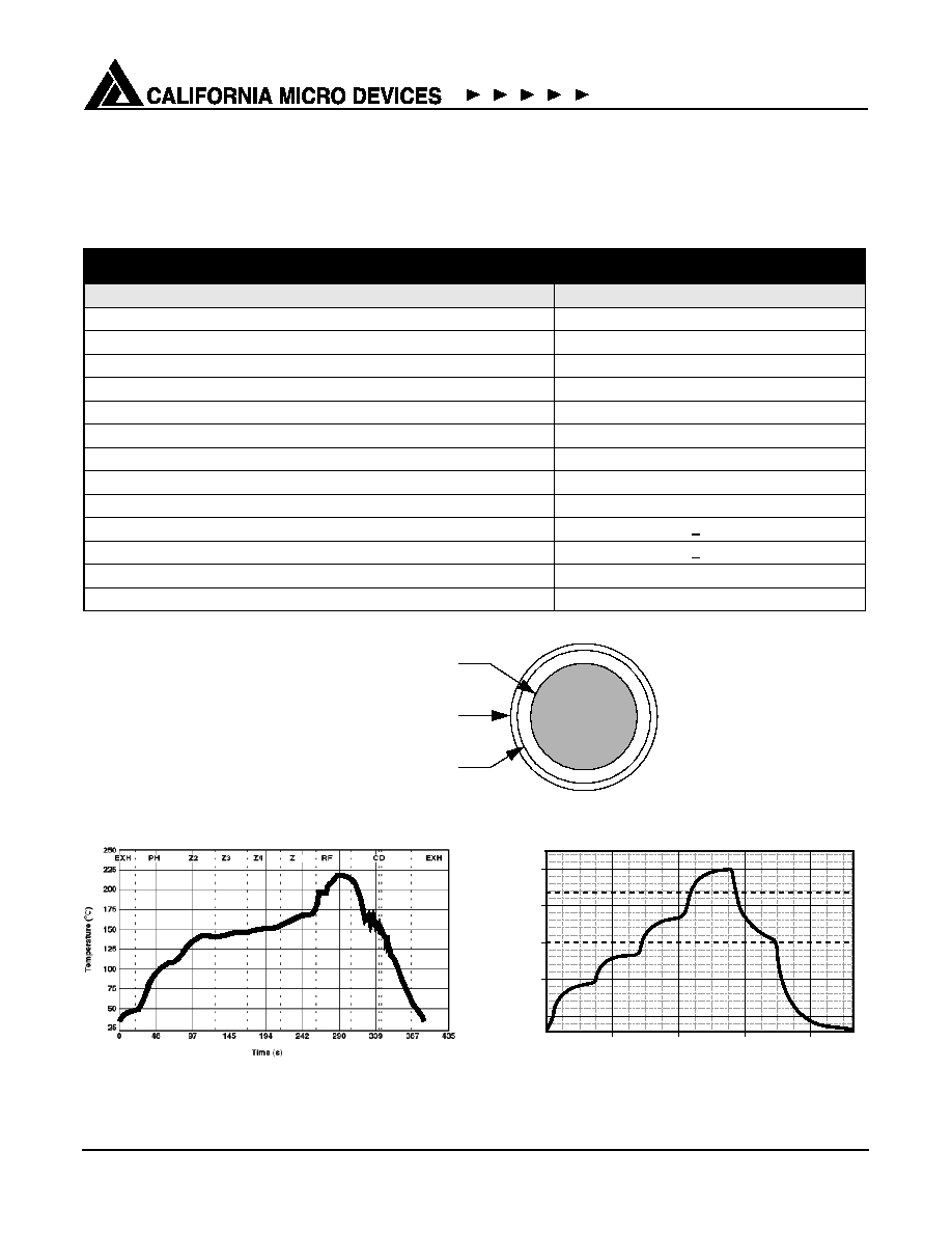
Figure 1. Recommended Non-Solder Mask Defined Pad Illustration
Figure 2. Eutectic (SnPb) Solder
Ball Reflow Profile
Figure 3. Lead-free (SnAgCu) Solder
Ball Reflow Profile
PRINTED CIRCUIT BOARD RECOMMENDATIONS
PARAMETER
VALUE
Pad Size on PCB
0.300mm
Pad Shape
Round
Pad Definition
Non-Solder Mask defined pads
Solder Mask Opening
0.350mm Round
Solder Stencil Thickness
0.125 - 0.150mm
Solder Stencil Aperture Opening (laser cut, 5% tapered walls)
0.360mm Round
Solder Flux Ratio
50/50 by volume
Solder Paste Type
No Clean
Pad Protective Finish
OSP (Entek Cu Plus 106A)
Tolerance -- Edge To Corner Ball
+50
µm
Solder Ball Side Coplanarity
+20
µm
Maximum Dwell Time Above Liquidous
60 seconds
Soldering Maximum Temperature
260∞C
Solder Mask Opening
0.350mm DIA.
Non-Solder Mask Defined Pad
0.300mm DIA.
Solder Stencil Opening
0.360mm DIA.
200
250
150
100
50
0
1:00.0
2:00.0
3:00.0
4:00.0
Time (minutes)
T
emperature (∞
C)
© 2003 California Micro Devices Corp. All rights reserved.
11/17/03
430 N. McCarthy Blvd., Milpitas, CA 95035-5112
L Tel: 408.263.3214
L Fax: 408.263.7846
L www.calmicro.com
5
CM1205
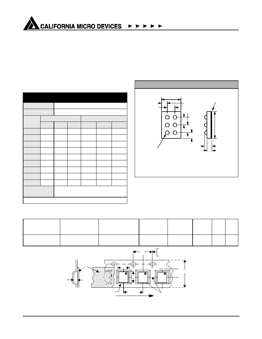
Mechanical Details
The CM1205 devices are packaged in custom Chip
Scale Packages (CSP).
CM1205-04CS/CP 6-bump CSP Mechanical Specifications
The CM1205-04CS/CP devices are packaged in a 6-
bump custom Chip Scale Package (CSP). Dimensions
are presented below.
Package Dimensions for CM1205-04CS/CP
6-bump Chip Scale Package
CSP Tape and Reel Specifications
Figure 4. Tape and Reel Mechanical Data
PACKAGE DIMENSIONS
Package
Custom CSP
Bumps
6
Dim
Millimeters
Inches
Min
Nom
Max
Min
Nom
Max
A1
1.109
1.154
1.199
0.0437
0.0454
0.0472
A2
1.759
1.804
1.849
0.0693
0.0710
0.0728
B1
0.645
0.650
0.655
0.0254
0.0256
0.0258
B2
0.645
0.650
0.655
0.0254
0.0256
0.0258
B3
0.645
0.650
0.655
0.0254
0.0256
0.0258
C1
0.202
0.252
0.302
0.0080
0.0099
0.0119
C2
0.202
0.252
0.302
0.0080
0.0099
0.0119
D1
0.638
0.707
0.776
0.0251
0.0278
0.0306
D2
0.394
0.445
0.495
0.0155
0.0175
0.0195
# per tape and
reel
3500 pieces
Controlling dimension: millimeters
Mechanical Package Diagrams
1
2
3
B
C1
B1
A1
B2
C2
0.35 DIA.
NOTE: DIMENSIONS IN MILLIMETERS
D1
D2
A2
BOTTOM VIEW
SIDE
VIEW
A
B3
63/37 Sn/Pb (Eutectic) or
SOLDER BUMPS
96.8/2.6/0.6 Sn/Ag/Cu (Lead-free)
OptiGuard
TM
Coating
PART NUMBER
CHIP SIZE (mm)
POCKET SIZE (mm)
B
0
X A
0
X K
0
TAPE WIDTH
W
REEL
DIA.
QTY
PER
REEL
P
0
P
1
CM1205-04CS/CP
1.804 X 1.154 X
0.644
1.98 X 1.32 X 0.91
8mm
178mm (7")
3500
4mm
4mm
Top
For tape feeder reference
Cover
Tape
P
1
only including draft.
Concentric around B.
K
o
Embossment
User Direction of Feed
±
0.2 mm
P
o
Center Lines
of Cavity
W
10 Pitches Cumulative
Tolerance On Tape
A
o
B
o