©
2004 California Micro Devices Corp. All rights reserved.
02/02/04
430 N. McCarthy Blvd., Milpitas, CA 95035-5112
L Tel: 408.263.3214
L Fax: 408.263.7846 L www.calmicro.com
1
CM1208-07/08
7 & 8-Channel High-Speed ESD Protection Arrays
Features
∑
Seven or eight channels of high-speed ESD pro-
tection
∑
Meets IEC-61000-4-2 Level 4 ESD protection
requirements (+8kV contact discharge)
∑
Meets IEC-61000-4-2 +15kV air discharge
requirements
∑
Low loading capacitance at 3pF typical
∑
Low
supply and leakage currents ≠ ideal for bat-
tery-powered devices
∑
Small MSOP-10 package
∑
Lead-free versions available
Applications
∑
High speed data line ESD protection
∑
DVI ports
∑
High resolution video (e.g. VGA ports)
∑
Expansion ports for Notebook/Handheld
Computers
∑
5V pseudo RS-232 ports
Product Description
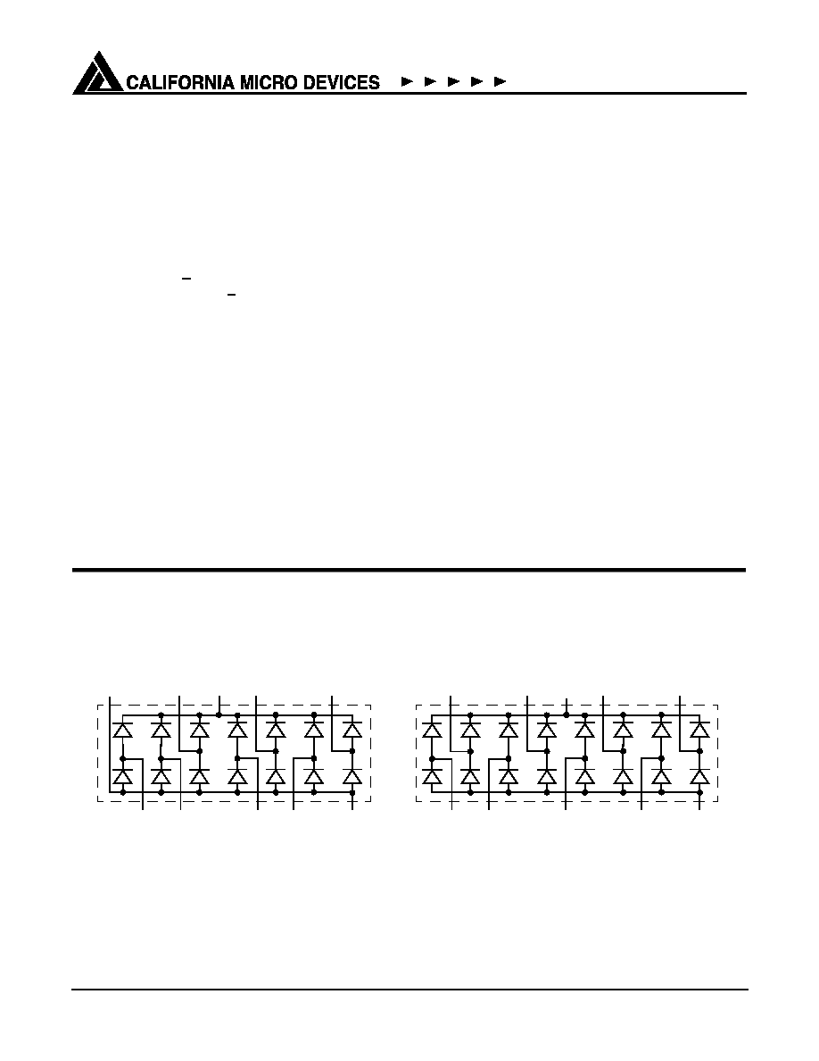
The CM1208-07/CM1208-08 is a diode array designed
to provide either 7 or 8 channels of ESD protection for
electronic components or sub-systems. Each channel
consists of a pair of diodes, which steers the ESD cur-
rent pulse to either the positive (V
P
) or negative (V
N
)
supply. The CM1208-07/08 devices will protect against
ESD pulses up to 15kV contact discharge per the Inter-
national Standard IEC61000-4-2.
These devices are particularly well-suited for portable
electronics (e.g.handheld and notebook computers)
because of its small package footprint, high ESD pro-
tection level, and low loading capacitance. They are
also suitable for protecting video output lines and I/O
ports in computers, set top boxes, digital TVs and
peripheral equipment.
The CM1208-07/CM1208-08 is housed in a 10 pin
MSOP package and is available with optional lead-free
finishing.
Electrical Schematics
CH3
V
N
CH6
CH4
CH5
CH1
V
P
CM1208-07
V
N
CH2
CH7
CH3
V
N
CH6
CH4
CH5
CH1
V
P
CM1208-08
CH8
CH2
CH7

©
2004 California Micro Devices Corp. All rights reserved.
2
430 N. McCarthy Blvd., Milpitas, CA 95035-5112
L Tel: 408.263.3214
L Fax: 408.263.7846 L www.calmicro.com
02/02/04
CM1208-07/08
Ordering Information
Note 1: Parts are shipped in Tape & Reel form unless otherwise specified.
PIN DESCRIPTIONS
DEVICE
PIN
NAME
TYPE
DESCRIPTION
-07,-08
1
CH 1
I/O
ESD Channel
-07,-08
2
CH 2
I/O
ESD Channel
-07,-08
3
CH 3
I/O
ESD Channel
-07,-08
4
CH 4
I/O
ESD Channel
-07,-08
5
V
N
GND
Negative voltage supply rail or ground reference rail
-07,-08
6
CH 5
I/O
ESD Channel
-07,-08
7
CH 6
I/O
ESD Channel
-07,-08
8
V
P
Supply
Positive voltage supply rail
-07,-08
9
CH 7
I/O
ESD Channel
-07
10
V
N
GND
Negative voltage supply rail or ground reference rail
-08
10
CH 8
I/O
ESD Channel
PACKAGE / PINOUT DIAGRAMS
Note: These drawings are not to scale.
10-pin MSOP
1
2
3
4
10
9
8
7
CH1
CH2
CH3
CH4
V
N
CH7
V
P
CH6
Top View
5
6
V
N
CH5
10-pin MSOP
1
2
3
4
10
9
8
7
CH1
CH2
CH3
CH4
CH8
CH7
V
P
CH6
Top View
5
6
V
N
CH5
CM1208-08MS
CM1208-07MS
CM1208-08MR
CM1208-07MR
PART NUMBERING INFORMATION
Pins
Package
Standard Finish
Lead-free Finish
Ordering Part
Number
1
Part Marking
Ordering Part
Number
1
Part Marking
10
MSOP
CM1208-07MS
0807
CM1208-07MR
807R
10
MSOP
CM1208-08MS
0808
CM1208-08MR
808R

©
2004 California Micro Devices Corp. All rights reserved.
02/02/04
430 N. McCarthy Blvd., Milpitas, CA 95035-5112
L Tel: 408.263.3214
L Fax: 408.263.7846
L www.calmicro.com
3
CM1208-07/08
Specifications
Note 1: Only one diode conducting at a time.
ABSOLUTE MAXIMUM RATINGS
PARAMETER
RATING
UNITS
Supply Voltage (V
P
- V
N
)
6.0
V
Diode Forward DC Current (Note 1)
20
mA
Operating Temperature Range
-40 to +85
∞C
Storage Temperature Range
-65 to +150
∞C
DC Voltage at any channel input
(V
N
- 0.5) to (V
P
+ 0.5)
V
Package Power Rating
MSOP Package
300
mW
STANDARD OPERATING CONDITIONS
PARAMETER
RATING
UNITS
Operating Temperature Range
-40 to +85
∞C
Operating Supply Voltage (V
P
- V
N
)
0 to 5.5
V
©
2004 California Micro Devices Corp. All rights reserved.
4
430 N. McCarthy Blvd., Milpitas, CA 95035-5112
L Tel: 408.263.3214
L Fax: 408.263.7846 L www.calmicro.com
02/02/04
CM1208-07/08
Note 1: All parameters specified at T
A
=-40 to +85∞C unless otherwise noted.
Note 2: These parameters guaranteed by design and characterization.
Note 3: From I/O pins to V
P
or V
N
only. A bypass capacitor between V
P and
V
N
is required. It is recommended that V
P
be bypassed
to V
N
with a 0.2
µF ceramic capacitor.
Note 4: Human Body Model per MIL-STD-883, Method 3015, C
Discharge
= 100pF, R
Discharge
= 1.5K
, V
P
= 5.0V, V
N
grounded.
Note 5: Standard IEC 61000-4-2 with C
Discharge
= 150pF, R
Discharge
= 330
, V
P
= 5.0V, V
N
grounded.
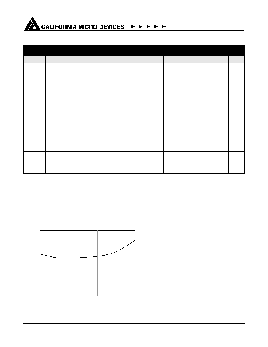
Performance Information
Typical Channel Input Capacitance vs. Channel Input Voltage at T
A
=25∞C
ELECTRICAL OPERATING CHARACTERISTICS
(SEE NOTE 1)
SYMBOL
PARAMETER
CONDITIONS
MIN
TYP
MAX
UNITS
I
P
Supply Current
(V
P
-V
N
)=5.0V
10
µA
V
F
Diode Forward Voltage
Top Diode
Bottom Diode
I
F
= 20mA; T
A
=25∞C
0.60
0.65
0.7
0.8
0.95
0.95
V
V
I
LEAK
Channel Leakage Current
T
A
=25∞C
±0.1
±1.0
µA
C
IN
Channel Input Capacitance
At 1 MHz, OSC Level =
30mV, V
P
=5V, V
N
=0V,
V
CH
=2.5V;
Note 2 applies
3
5
pF
V
ESD
ESD Protection
Peak Discharge Voltage at any chan-
nel input
a) Contact discharge per
IEC 61000-4-2 standard
b) Human Body Model, MIL-
STD-883, Method 3015
Notes 2, 3 & 5
Notes 2, 3 & 4
±8
±15
kV
kV
V
CL
Channel Clamp Voltage
Positive Transients
Negative Transients
At 8kV ESD HBM;
T
A
=25∞C; Note 2, 3 & 4
V
P
+ 5.0
V
N
- 5.0
V
V
T y p ic a l V a r ia t io n o f C
IN
vs. V
IN
(VP = 5V, VN = 0V, 0.2 µF chip capacitor between VP and VN)
0
1
2
3
4
5
0
1
2
3
4
5
Input Voltage
Input Capacitance (p
F)

©
2004 California Micro Devices Corp. All rights reserved.
02/02/04
430 N. McCarthy Blvd., Milpitas, CA 95035-5112
L Tel: 408.263.3214
L Fax: 408.263.7846
L www.calmicro.com
5
CM1208-07/08
Application Information
Design Considerations
In order to realize the maximum protection against
ESD pulses, care must be taken in the PCB layout to
minimize parasitic series inductances on the Supply/
Ground rails as well as the signal trace segment
between the signal input (typically a connector) and the
ESD protection device. Refer to
Figure 1
, which illus-
trates an example of a positive ESD pulse striking an
input channel. The parasitic series inductance back to
the power supply is represented by L
1
and
L
2
. The volt-
age V
CL
on the line being protected is:
V
CL
= Fwd voltage drop of D
1
+ V
SUPPLY
+ L
1
x d(I
ESD
)
/
dt
+ L
2
x d(I
ESD
)
/
dt
where I
ESD
is the ESD current pulse, and V
SUPPLY
is
the positive supply voltage.
An ESD current pulse can rise from zero to its peak
value in a very short time. As an example, a level 4
contact discharge per the IEC61000-4-2 standard
results in a current pulse that rises from zero to 30
Amps in 1ns. Here d(I
ESD
)/dt can be approximated by
I
ESD
/
t, or 30/(1x10
-9
). So just 10nH of series induc-
tance (L
1
and
L
2
combined) will lead to a 300V incre-
ment in V
CL
!
Similarly for negative ESD pulses, parasitic series
inductance from the V
N
pin to the ground rail will lead
to drastically increased negative voltage on the line
being protected.
Another consideration is the output impedance of the
power supply for fast transient currents. Most power
supplies exhibit a much higher output impedance to
fast transient current spikes. In the V
CL
equation
above, the V
SUPPLY
term, in reality, is given by (V
DC
+
I
ESD
x R
OUT
), where V
DC
and R
OUT
are the nominal
supply DC output voltage and effective output imped-
ance of the power supply respectively. As an example,
a R
OUT
of 1 ohm would result in a 10V increment in
V
CL
for a peak I
ESD
of 10A.
To mitigate these effects, a high frequency bypass
capacitor should be connected between the V
P
pin of
the ESD Protection Array and the ground plane. The
value of this bypass capacitor should be chosen such
that it will absorb the charge transferred by the ESD
pulse with minimal change in V
P
. Typically a value in
the 0.1µF to 0.2µF range is adequate for IEC-61000-4-
2 level 4 contact discharge protection (8kV). For higher
ESD voltages, the bypass capacitor should be
increased accordingly. Ceramic chip capacitors
mounted with short printed circuit board traces are
good choices for this application. Electrolytic capaci-
tors should be avoided as they have poor high fre-
quency characteristics. For extra protection, connect a
zener diode in parallel with the bypass capacitor to mit-
igate the effects of the parasitic series inductance
inherent in the capacitor. The breakdown voltage of the
zener diode should be slightly higher than the maxi-
mum supply voltage.
As a general rule, the ESD Protection Array should be
located as close as possible to the point of entry of
expected electrostatic discharges. The power supply
bypass capacitor mentioned above should be as close
to the V
P
pin of the Protection Array as possible, with
minimum PCB trace lengths to the power supply,
ground planes and between the signal input and the
ESD device to minimize stray series inductance.
Additional Information
See also California Micro Devices Application Note
AP209, "Design Considerations for ESD Protection."
Figure 1. Application of Positive ESD Pulse between Input Channel and Ground
N
L
2
L
1
V
P
V
PATH OF ESD CURRENT PULSE I
ONE
CHANNEL
OF
CM1208
CHANNEL
INPUT
GROUND RAIL
CHASSIS GROUND
POSITIVE SUPPLY RAIL
SYSTEM OR
CIRCUITRY
BEING
PROTECTED
LINE BEING
PROTECTED
ESD
D
1
2
D
0A
20A
V
CL