© 2006 California Micro Devices Corp. All rights reserved.
02/03/06
490 N. McCarthy Blvd., Milpitas, CA 95035-5112
Tel: 408.263.3214
Fax: 408.263.7846
www.cmd.com
1
CM1220
4 and 8-Channel ESD Protection Arrays in CSP
Features
∑
4 and 8 channels of ESD protection
∑
OptiGuard
TM
coated for improved reliability
∑
±
15kV ESD protection on each channel
(IEC 61000-4-2 Level 4, contact discharge)
∑
±
30kV ESD protection on each channel (HBM)
∑
Chip Scale Package features extremely low
lead inductance for optimum ESD protection
∑
5 bump, 0.960mm X 1.330mm CSP footprint
for CM1220-04
∑
10 bump, 1.960mm X 1.330mm CSP footprint
for CM1220-08
∑
Lead-free version available
Applications
∑
LCD and camera datalines in mobile handsets
∑
I/O port protection for mobile handsets, notebook
computers, PDAs, etc.
∑
Keypads and buttons
∑
Wireless handsets
∑
Handheld PCs/PDAs
∑
LCD and camera modules
Product Description
California Micro Devices' CM1220 ESD protection
arrays are available in four and eight channel configu-
rations. Each ESD channel features a nominal capaci-
tance of 14pF making these devices ideal for
protecting high speed I/O ports and LCD and camera
data lines without significantly affecting signal integrity.
The CM1220 integrates avalanche-type ESD diodes
on every channel, providing a very high level of protec-
tion for sensitive electronic components that may be
subjected to electrostatic discharge (ESD). These
diodes safely dissipate ESD strikes of
±
15kV, exceed-
ing the maximum requirement of the IEC61000-4-2
international standard. Using the MIL-STD-883
(Method 3015) specification for Human Body Model
(HBM) ESD, these devices protect for contact dis-
charges at greater than
±
30kV.
These devices are particularly well-suited for portable
electronics (e.g. wireless handsets, PDAs, notebook
computers) because of their small package and easy-
to-use pin assignments. In particular, the CM1220 is
ideal for protecting high speed I/O ports and data and
control lines for the LCD display and camera interface
in mobile handsets.
These devices incorporate CMD's OptiGuard
TM
coating
for improved reliability at assembly. The CM1220 is
available in a space-saving, low-profile Chip Scale
Packages with optional lead-free finishing.
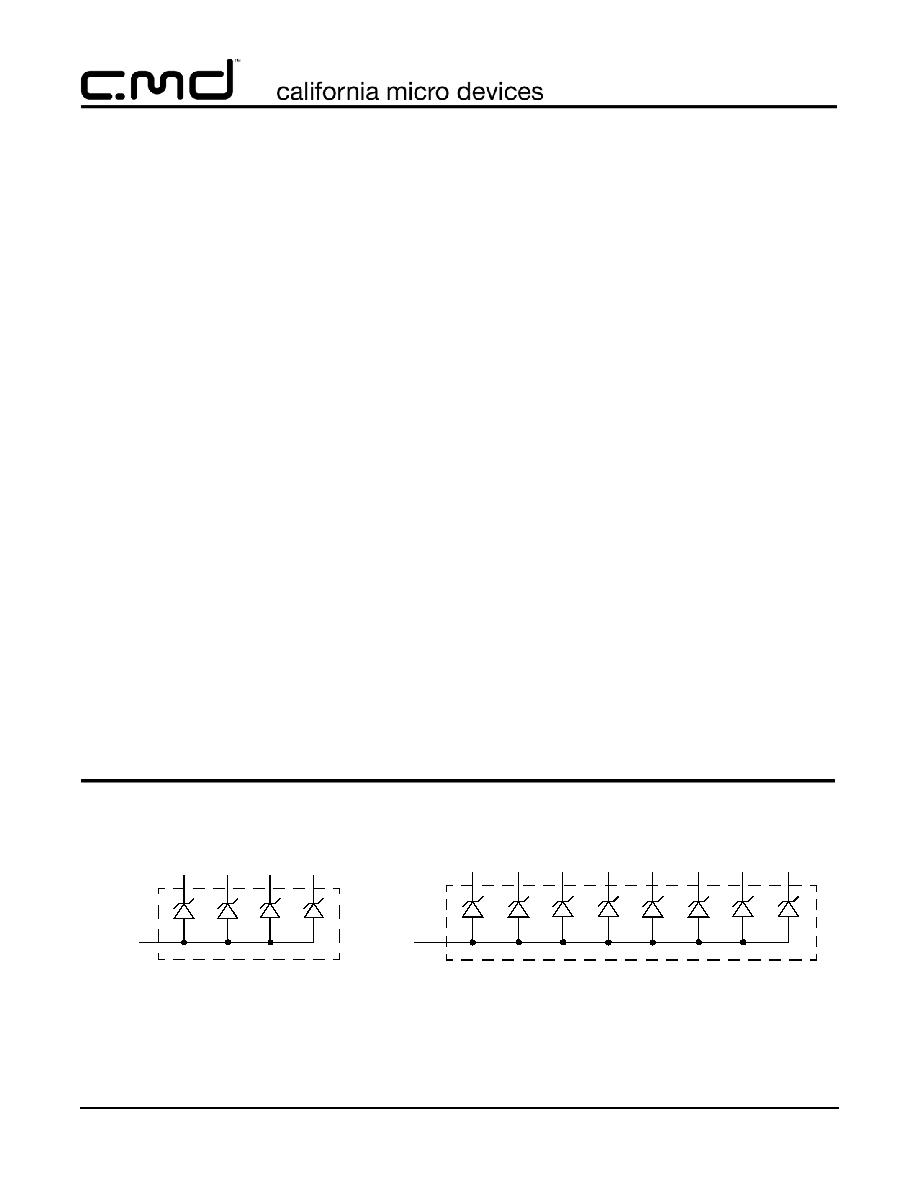
Electrical Schematic
B2, B6
ESD_1
GND
A5
A7
A1
A3
ESD_2 ESD_3 ESD_4 ESD_5
C5
C7
C1
C3
ESD_6 ESD_7 ESD_8
CM1220-08
B2
ESD_1
GND
C1
C3
A1
A3
ESD_2 ESD_3 ESD_4
CM1220-04
© 2006 California Micro Devices Corp. All rights reserved.
2
490 N. McCarthy Blvd., Milpitas, CA 95035-5112
Tel: 408.263.3214
Fax: 408.263.7846
www.cmd.com
02/03/06
CM1220
Ordering Information
Note 1: Parts are shipped in Tape & Reel form unless otherwise specified.
Note 2: Lead-free devices are specified by using a "
+
" character for the top side orientation mark.
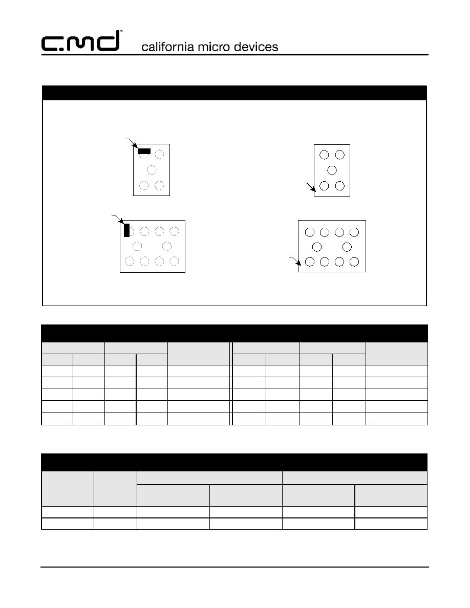
PIN DESCRIPTIONS
CM1220-08
CM1220-04
DESCRIPTION
CM1220-08
CM1220-04
DESCRIPTION
PINS
NAME
PINS
NAME
PINS
NAME
PINS
NAME
A1
ESD1
A1
ESD1
ESD Channel
C1
ESD5
C1
ESD3
ESD Channel
A3
ESD2
A3
ESD2
ESD Channel
C3
ESD6
C3
ESD4
ESD Channel
A5
ESD3
-
-
ESD Channel
C5
ESD7
-
-
ESD Channel
A7
ESD4
-
-
ESD Channel
C7
ESD8
-
-
ESD Channel
B2
GND
B2
GND
Device Ground
B6
GND
-
-
Device Ground
L208
5
1
7
3
6
2
C
B
A
Orientation
Marking(see note 2)
A3
A1
Orientation
Marking
A5
B6
B2
C5
C3
A7
C7
C1
A1
A1
A3
C3
C1
B2
Orientation
Marking
A1
J
2 3
1
C
B
A
Orientation
Marking
(see note 2)
PACKAGE / PINOUT DIAGRAMS
CM1220-04
5 Bump CSP Package
TOP VIEW
BOTTOM VIEW
(Bumps Down View)
(Bumps Up View)
Notes:
1) These drawings are not to scale.
2) Lead-free devices are specified by using a "
+
" character for the top side orientation mark.
CM1220-08
10 Bump CSP Package
with OptiGuard
TM
with OptiGuard
TM
PART NUMBERING INFORMATION
Bumps
Package
Standard Finish
Lead-free Finish
2
Ordering Part
Number
1
Part Marking
Ordering Part
Number
1
Part Marking
5
CSP
CM1220-04CS
J
CM1220-04CP
J
10
CSP
CM1220-08CS
L208
CM1220-08CP
L208
© 2006 California Micro Devices Corp. All rights reserved.
02/03/06
490 N. McCarthy Blvd., Milpitas, CA 95035-5112
Tel: 408.263.3214
Fax: 408.263.7846
www.cmd.com
3
CM1220
Specifications
Note 1: T
A
=25
∞
C unless otherwise specified.
Note 2: ESD applied to input and output pins with respect to GND, one at a time. Unused pins are left open. These parameters are
guaranteed by design and characterization.
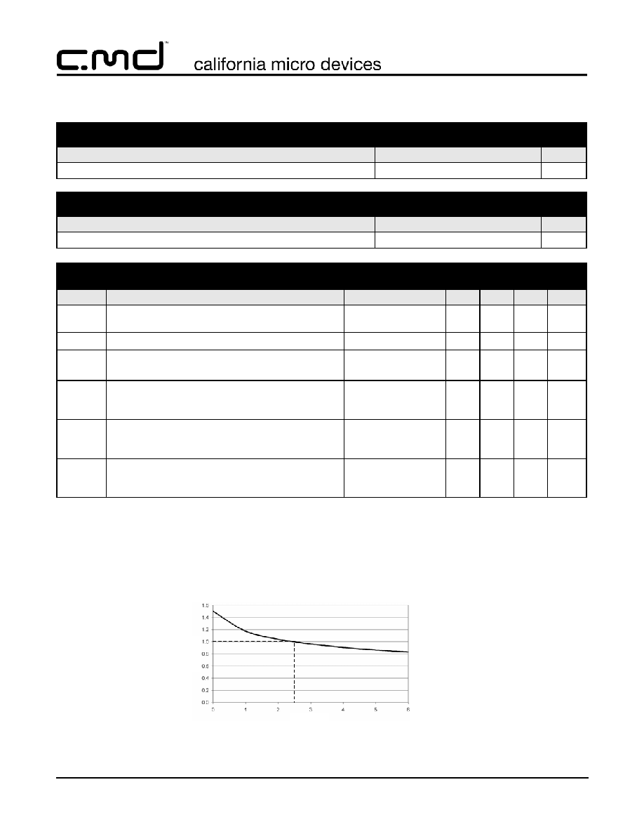
Performance Information
Diode Characteristics (nominal conditions unless specified otherwise)
Figure 1. Typical Diode Capacitance VS. Input Voltage (normalized to 2.5VDC)
ABSOLUTE MAXIMUM RATINGS
PARAMETER
RATING
UNITS
Storage Temperature Range
-65 to +150
∞C
STANDARD OPERATING CONDITIONS
PARAMETER
RATING
UNITS
Operating Temperature Range
-40 to +85
∞C
ELECTRICAL OPERATING CHARACTERISTICS
(SEE NOTE 1)
SYMBOL PARAMETER
CONDITIONS
MIN
TYP
MAX
UNITS
C
DIODE
Diode (Channel) Capacitance
At 2.5VDC Reverse
Bias, 1MHz, 30mVAC
11
14
17
pF
V
DIODE
Diode Standoff Voltage
I
DIODE
= 10
A
6.0
V
I
LEAK
Diode Leakage Current
V
IN
=
+
3.3V
(reverse bias voltage)
0.1
1
A
V
SIG
Signal Clamp Voltage
Positive Clamp
Negative Clamp
I
DIODE
= 10mA
5.6
-1.5
6.8
-0.8
9.0
-0.4
V
V
V
ESD
In-system ESD Withstand Voltage
a) Human Body Model, MIL-STD-883, Method 3015
b) Contact Discharge per IEC 61000-4-2
Note 2
±30
±15
kV
kV
R
DYN
Dynamic Resistance
Positive
Negative
2.3
0.9
C
a
pacitanc
e
(
Normaliz
ed)
DC Voltage
© 2006 California Micro Devices Corp. All rights reserved.
4
490 N. McCarthy Blvd., Milpitas, CA 95035-5112
Tel: 408.263.3214
Fax: 408.263.7846
www.cmd.com
02/03/06
CM1220
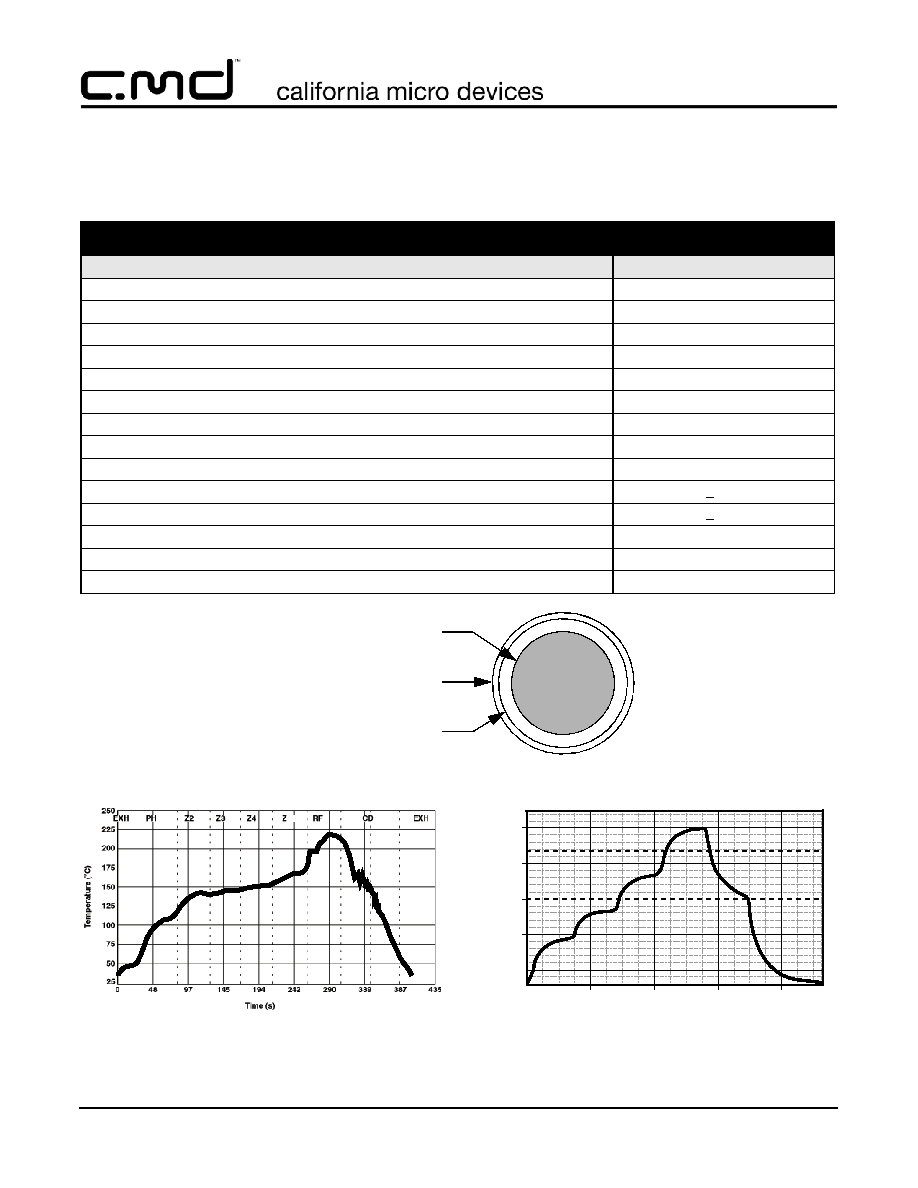
Application Information
Refer to Application Note AP-217, "The Chip Scale Package", for a detailed description of Chip Scale Packages
offered by California Micro Devices.
Figure 2. Recommended Non-Solder Mask Defined Pad Illustration
Figure 3. Eutectic (SnPb) Solder
Ball Reflow Profile
Figure 4. Lead-free (SnAgCu) Solder
Ball Reflow Profile
PRINTED CIRCUIT BOARD RECOMMENDATIONS
PARAMETER
VALUE
Pad Size on PCB
0.275mm
Pad Shape
Round
Pad Definition
Non-Solder Mask defined pads
Solder Mask Opening
0.325mm Round
Solder Stencil Thickness
0.125mm - 0.150mm
Solder Stencil Aperture Opening (laser cut, 5% tapered walls)
0.330mm Round
Solder Flux Ratio
50/50 by volume
Solder Paste Type
No Clean
Pad Protective Finish
OSP (Entek Cu Plus 106A)
Tolerance -- Edge To Corner Ball
+50
m
Solder Ball Side Coplanarity
+20
m
Maximum Dwell Time Above Liquidous
60 seconds
Maximum Soldering Temperature for Eutectic Devices using a Eutectic Solder Paste
240∞C
Maximum Soldering Temperature for Lead-free Devices using a Lead-free Solder Paste
260∞C
Solder Mask Opening
0.325mm DIA.
Non-Solder Mask Defined Pad
0.275mm DIA.
Solder Stencil Opening
0.330mm DIA.
200
250
150
100
50
0
1:00.0
2:00.0
3:00.0
4:00.0
Time (minutes)
T
emperature
(∞
C)
© 2006 California Micro Devices Corp. All rights reserved.
02/03/06
490 N. McCarthy Blvd., Milpitas, CA 95035-5112
Tel: 408.263.3214
Fax: 408.263.7846
www.cmd.com
5
CM1220
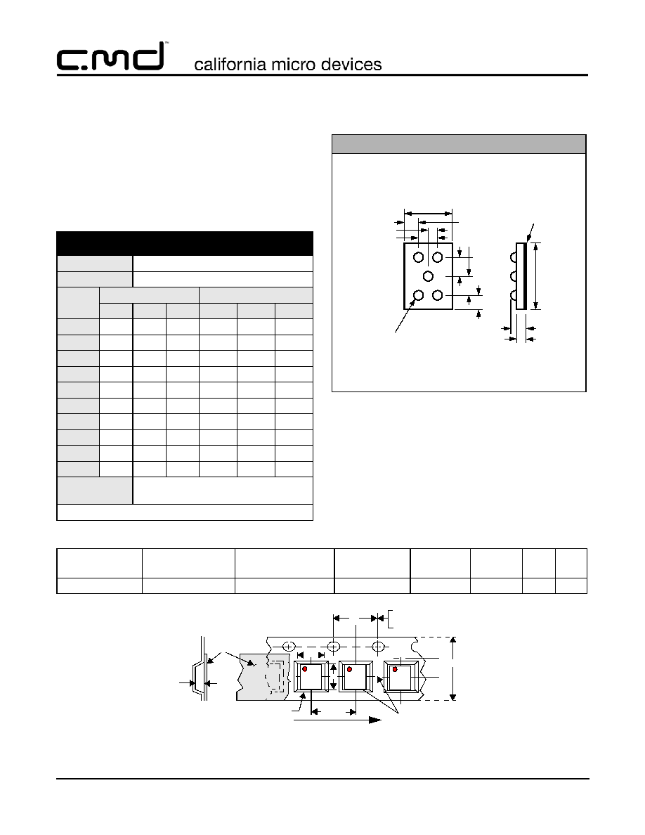
Mechanical Details
The CM1220 is supplied in custom Chip Scale Pack-
ages (CSP) depending on the channel count. Dimen-
sions for these packages are presented in the following
pages.
CM1220-04CS/CP Mechanical Specifications
Mechanical dimensions for the CM1220-04CS/CP are
presented below.
Package Dimensions for
CM1220-04CS/CP Chip Scale Package
CSP Tape and Reel Specifications
Figure 5. Tape and Reel Mechanical Data
PACKAGE DIMENSIONS
Package
Custom CSP
Bumps
5
Dim
Millimeters
Inches
Min
Nom
Max
Min
Nom
Max
A1
0.915 0.960 1.005 0.0360 0.0378 0.0396
A2
1.285 1.330 1.375 0.0506 0.0524 0.0541
B1
0.495 0.500 0.505 0.0195 0.0197 0.0199
B2
0.245 0.250 0.255 0.0096 0.0098 0.0100
B3
0.430 0.435 0.440 0.0169 0.0171 0.0173
B4
0.430 0.435 0.440 0.0169 0.0171 0.0173
C1
0.180 0.230 0.280 0.0071 0.0091 0.0110
C2
0.180 0.230 0.280 0.0071 0.0091 0.0110
D1
0.575 0.644 0.714 0.0226 0.0254 0.0281
D2
0.368 0.419 0.470 0.0145 0.0165 0.0185
# per tape and
reel
3500 pieces
Controlling dimension: millimeters
Mechanical Package Diagrams
DIMENSIONS IN MILLIMETERS
A
B
C
1 2
C1
B1
A1
B3
C2
D1
D2
A2
BOTTOM VIEW
SIDE
VIEW
3
B2
B4
0.30 DIA.
63/37 Sn/Pb (Eutectic) or
SOLDER BUMPS
96.8/2.6/0.6 Sn/Ag/Cu (Lead-free)
OptiGuard
TM
Coating
OptiGuard
TM
Coated CSP
PART NUMBER
CHIP SIZE (mm)
POCKET SIZE (mm)
B
0
X A
0
X K
0
TAPE WIDTH
W
REEL
DIAMETER
QTY PER
REEL
P
0
P
1
CM1220-04
1.33 X 0.96 X 0.644
1.42 X 1.07 X 0.740
8mm
178mm (7")
3500
4mm
4mm
Top
For tape feeder reference
Cover
Tape
P
1
only including draft.
Concentric around B.
K
o
Embossment
User Direction of Feed
±
0.2 mm
P
o
Center Lines
of Cavity
W
10 Pitches Cumulative
Tolerance On Tape
A
o
B
o