
©
2004 California Micro Devices Corp. All rights reserved.
08/16/04
430 N. McCarthy Blvd., Milpitas, CA 95035-5112
Tel: 408.263.3214
Fax: 408.263.7846
www.calmicro.com
1
CM1406
4 Channel EMI Filter Array with ESD Protection
Features
∑
Four channels of EMI filtering with ESD protection
∑
Greater than 30dB of attenuation from 800MHz to
3GHz
∑
±15kV ESD protection (IEC 61000-4-2, contact
discharge)
∑
±30kV ESD protection (HBM)
∑
8-lead TDFN package (2mm x 2mm), 0.5mm pitch
∑
Lead-free version available
Applications
∑
I/O port protection for mobile handsets, notebook
computers, PDAs etc.
∑
EMI filtering for data ports in cell phones, PDAs or
notebook computers.
∑
EMI filtering for LCD and chip-to-chip data lines
Product Description
California Micro Devices's CM1406 is an EMI filter
array with ESD protection, which integrates 4 pi filters
(C-R-C). The CM1406 has component values of 15pF-
200
-15pF. The parts include ESD protection diodes
on every pin, which provide a very high level of protec-
tion for sensitive electronic components that may be
subjected to electrostatic discharge (ESD). The ESD
diodes connected to the filter ports are designed and
characterized to safely dissipate ESD strikes of
±15kV
contact discharge, twice the specification requirement
of the IEC 61000-4-2, Level 4 international standard.
Using the MIL-STD-883 (Method 3015) specification
for Human Body Model (HBM) ESD, the pins are pro-
tected for contact discharges at greater than
±30kV.
This device is particularly well suited for portable elec-
tronics (e.g. mobile handsets, PDAs, notebook comput-
ers) because of its small package format and easy-to-
use pin assignments. In particular, the CM1406 is
ideal for EMI filtering and protecting data lines from
ESD in wireless handsets.
The CM1406 is available in a space-saving, low-profile,
8-lead, 2mm x 2mm TDFN package. It is fabricated
with California Micro Devices' Centurion
TM
process and
available with optional lead-free finishing.
Electrical Schematic
* See Package/Pinout Diagram for expanded pin information.
1 of 4 EMI Filtering + ESD Channels
200
15pF
15pF
FILTERn*
GND
FILTERn*
©
2004 California Micro Devices Corp. All rights reserved.
2
430 N. McCarthy Blvd., Milpitas, CA 95035-5112
Tel: 408.263.3214
Fax: 408.263.7846
www.calmicro.com
08/16/04
CM1406
Ordering Information
Note 1: Parts are shipped in Tape & Reel form unless otherwise specified.
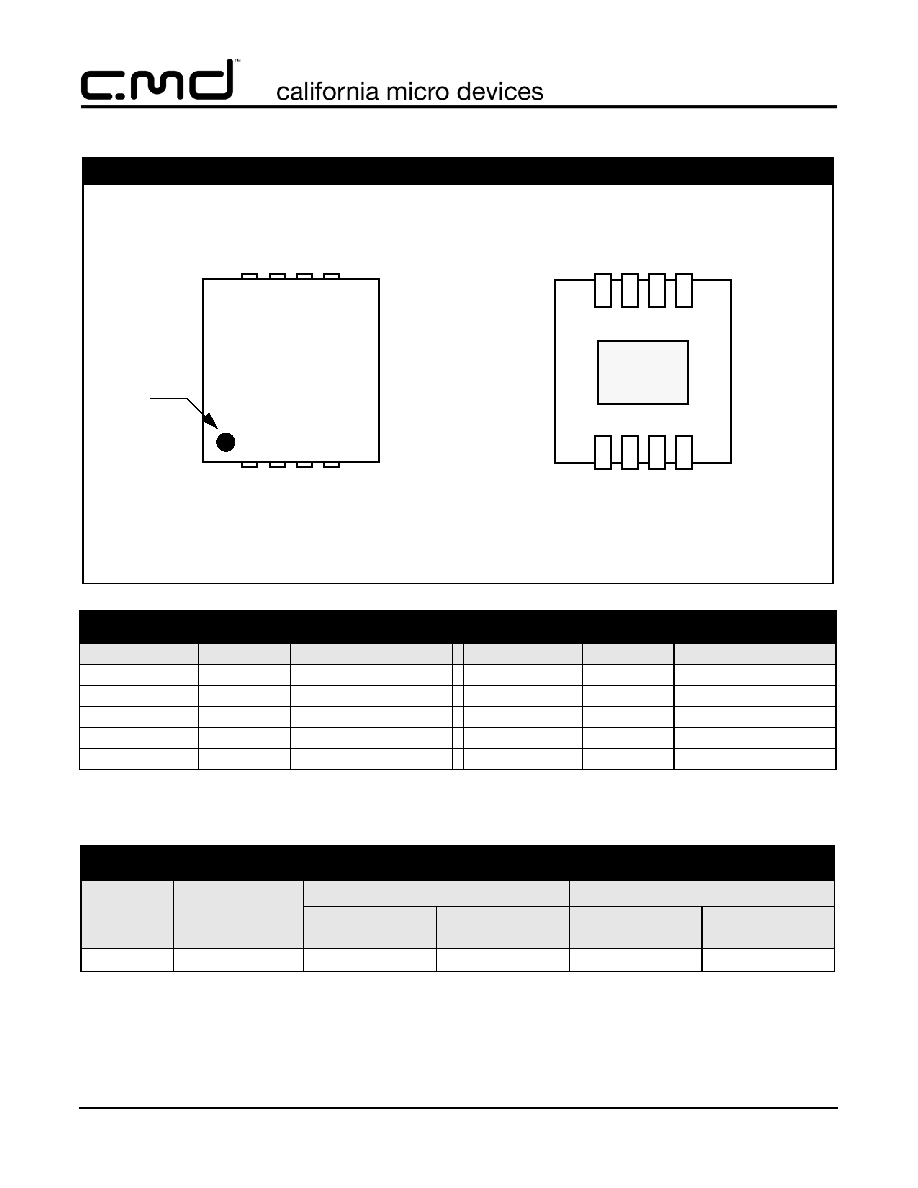
PACKAGE / PINOUT DIAGRAMS
Notes:
BOTTOM VIEW
(Pins Up View)
TOP VIEW
(Pins Down View)
CM1406
1) This drawing is not to scale.
8-Lead TDFN Package
Pin 1
N06
2) See Ordering Information section below for device specific marking.
GND
5
6
7
8
4
3
2
1
4
3
2
1
5
6
7
8
PAD
Marking
4x
PIN DESCRIPTIONS
PIN(s)
NAME
DESCRIPTION
PIN(s)
NAME
DESCRIPTION
1
FILTER1
Filter Channel 1
5
FILTER4
Filter Channel 4
2
FILTER2
Filter Channel 2
6
FILTER3
Filter Channel 3
3
FILTER3
Filter Channel 3
7
FILTER2
Filter Channel 2
4
FILTER4
Filter Channel 4
8
FILTER1
Filter Channel 1
GND Pad
GND
Device Ground
PART NUMBERING INFORMATION
Leads/Pins
Package
Standard Finish
Lead-free Finish
Ordering Part
Number
1
Part Marking
Ordering Part
Number
1
Part Marking
8
TDFN-08
CM1406-04DF
N06 4F
CM1406-04DE
N06 4E
©
2004 California Micro Devices Corp. All rights reserved.
08/16/04
430 N. McCarthy Blvd., Milpitas, CA 95035-5112
Tel: 408.263.3214
Fax: 408.263.7846
www.calmicro.com
3
CM1406
Specifications
Note 1: T
A
=25
∞
C unless otherwise specified.
Note 2: ESD applied to input and output pins with respect to GND, one at a time.
Note 3: Clamping voltage is measured at the opposite side of the EMI filter to the ESD pin. For example, if ESD is applied to Pin 1,
then clamping voltage is measured at Pin 8.
Note 4: Unused pins are left open
Note 5: These parameters are guaranteed by design and characterization.
ABSOLUTE MAXIMUM RATINGS
PARAMETER
RATING
UNITS
Storage Temperature Range
-65 to +150
∞C
DC Power per Resistor
100
mW
DC Package Power Rating
300
mW
STANDARD OPERATING CONDITIONS
PARAMETER
RATING
UNITS
Operating Temperature Range
-40 to +85
∞C
ELECTRICAL OPERATING CHARACTERISTICS
(SEE NOTE 1)
SYMBOL
PARAMETER
CONDITIONS
MIN
TYP
MAX
UNITS
R
Resistance
160
200
240
C
Capacitance
At 2.5V DC, 1MHz, 30mV
AC
12
15
18
pF
V
DIODE
Diode Standoff Voltage
I
DIODE
= 10
µA
5.5
V
I
LEAK
Diode Leakage Current (reverse bias)
V
DIODE
= 3.3V
100
nA
V
SIG
Signal Voltage
Positive Clamp
Negative Clamp
I
LOAD
= 10mA
I
LOAD
= -10mA
5.6
-0.4
6.8
-0.8
9.0
-1.5
V
V
V
ESD
In-system ESD Withstand Voltage
a) Human Body Model, MIL-STD-883,
Method 3015
b) Contact Discharge per IEC 61000-4-2
Level 4
Notes 2,4 and 5
±30
±15
kV
kV
V
CL
Clamping Voltage during ESD Discharge
MIL-STD-883 (Method 3015), 8kV
Positive Transients
Negative Transients
Notes 2,3,4 and 5
+12
-7
V
V
f
C
Cut-off Frequency
Z
SOURCE
=50
, Z
LOAD
=50
R = 200
, C = 15pF
105
MHz

©
2004 California Micro Devices Corp. All rights reserved.
4
430 N. McCarthy Blvd., Milpitas, CA 95035-5112
Tel: 408.263.3214
Fax: 408.263.7846
www.calmicro.com
08/16/04
CM1406
Performance Information
Typical Filter Performance (nominal conditions unless specified otherwise, 0V DC Bias, 50 Ohm Environment)
Figure 1. Channel 1 (Pin 1 - Pin 8) EMI Filter Performance
Figure 2. Channel 2 (Pin 2 - Pin 7) EMI Filter Performance

©
2004 California Micro Devices Corp. All rights reserved.
08/16/04
430 N. McCarthy Blvd., Milpitas, CA 95035-5112
Tel: 408.263.3214
Fax: 408.263.7846
www.calmicro.com
5
CM1406
Performance Information (cont'd)
Typical Filter Performance (nominal conditions unless specified otherwise, 0V DC Bias, 50 Ohm Environment)
Figure 3. Channel 3 (Pin 3 - Pin 6) EMI Filter Performance
Figure 4. Channel 4 (Pin 4 - Pin 5) EMI Filter Performance

©
2004 California Micro Devices Corp. All rights reserved.
6
430 N. McCarthy Blvd., Milpitas, CA 95035-5112
Tel: 408.263.3214
Fax: 408.263.7846
www.calmicro.com
08/16/04
CM1406
Performance Information (cont'd)
Figure 5. Filter Capacitance vs. Input Voltage over Temperature
(normalized to capacitance at 2.5VDC and 25∞C)
©
2004 California Micro Devices Corp. All rights reserved.
08/16/04
430 N. McCarthy Blvd., Milpitas, CA 95035-5112
Tel: 408.263.3214
Fax: 408.263.7846
www.calmicro.com
7
CM1406
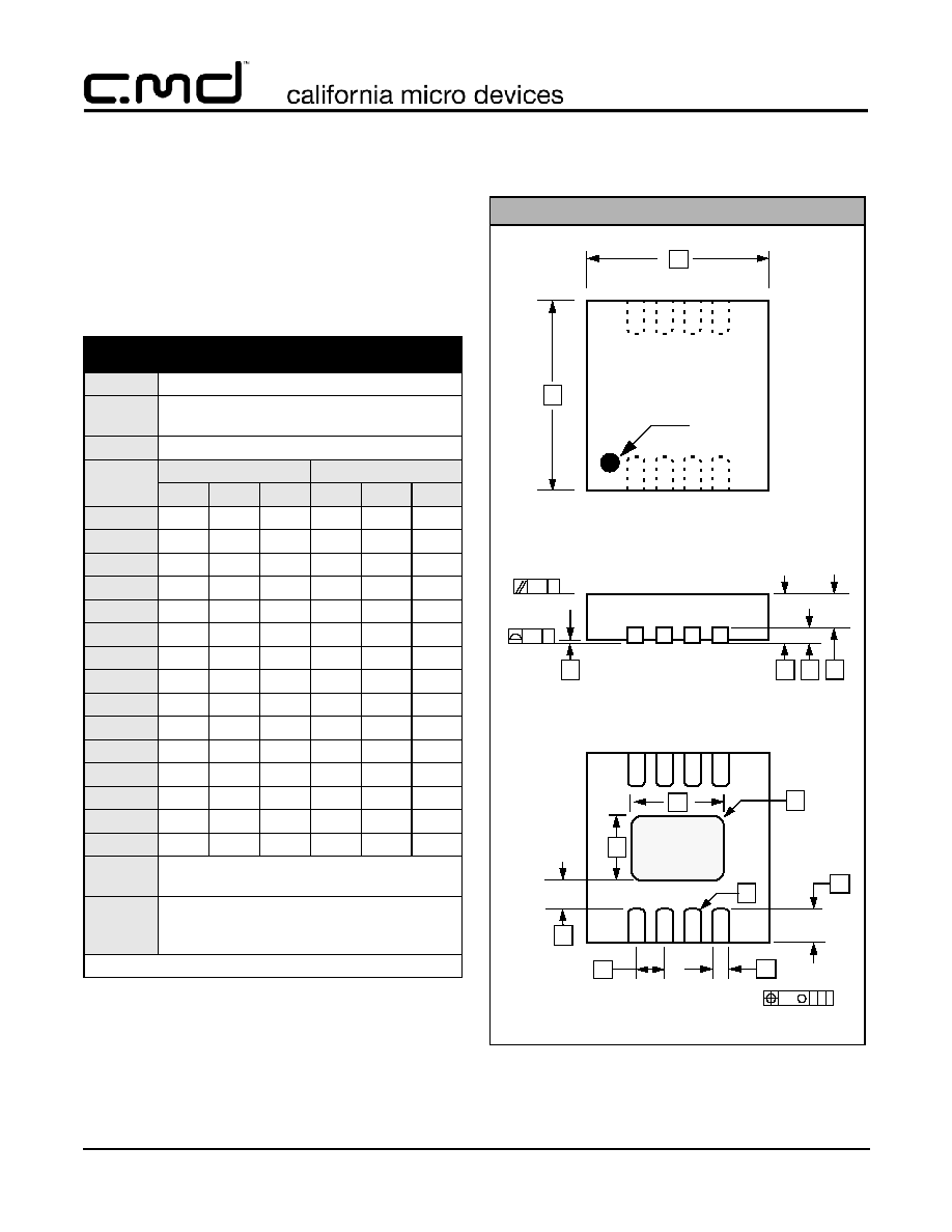
Mechanical Details
TDFN-08 Mechanical Specifications
Dimensions for CM1406 device packaged in an 8-lead
TDFN package are presented below.
For complete information on the TDFN-08 package,
see the California Micro Devices TDFN Package Infor-
mation document.
This package is compliant with JEDEC standard MO-229, variation
VCCD-3 with exception of the "D2" and "E2" dimensions as called
out in the table above and the "r1" dimension which is not specified in
the MO-229 standard.
Package Dimensions for 8-Lead TDFN
PACKAGE DIMENSIONS
Package
TDFN
JEDEC
No.
MO-229 (Var. VCCD-3)
Leads
8
Dim.
Millimeters
Inches
Min
Nom
Max
Min
Nom
Max
A
0.80
0.90
1.00
0.031
0.035
0.039
A1
0.00
0.02
0.05
0.000
0.001
0.002
A2
0.55
0.65
0.80
0.022
0.026
0.031
A3
0.20
0.008
b
0.18
0.25
0.30
0.007
0.010
0.012
D
2.00
0.079
D2
0.88
0.98
1.08
0.035
0.039
0.043
E
2.00
0.079
E2
0.46
0.56
0.66
0.018
0.022
0.026
e
0.50
0.020
K
0.20
0.008
L
0.20
0.30
0.45
0.008
0.012
0.018
L2
0.13
0.005
R
0.075
0.003
r1
0.075
0.003
# per
tube
NA
# per
tape and
reel
3000 pieces
Controlling dimension: millimeters
Mechanical Package Diagrams
BOTTOM VIEW
A
A3
A1
0.10 C
0.08 C
SIDE VIEW
TOP VIEW
b
L
0.10
C A B
M
8X
D2
E2
e
GND PAD
D
E
Pin 1
Marking
4
3
2
1
5
6
7
8
A2
K
R
r1
5
6
7
8
3
2
1
4