© 2006 California Micro Devices Corp. All rights reserved.
06/16/06
490 N. McCarthy Blvd., Milpitas, CA 95035-5112
Tel: 408.263.3214
Fax: 408.263.7846
www.cmd.com
1
CM1409
PRELIMINARY
LCD and Camera EMI Filter Array with ESD Protection
Features
∑
Six and eight channels of EMI filtering with inte-
grated ESD protection
∑
Pi-style EMI filters in a capacitor-resistor-capacitor
(C-R-C) network
∑
±15kV ESD protection on each channel
(IEC 61000-4-2 Level 4, contact discharge)
∑
±30kV ESD protection on each channel (HBM)
∑
Greater than 35dB attenuation (typical) at 1 GHz
∑
TDFN package with 0.50mm lead pitch:
∑ 6-ch. = 12-lead TDFN
∑ 8-ch. = 16-lead TDFN
∑
Tiny TDFN package size:
∑ 12-lead: 3.0mm x 1.35mm (two styles)
∑ 16-lead: 4.0mm x 1.60mm
∑
Increased robustness against vertical impacts
during manufacturing process
∑
Lead-free finishing
Applications
∑
LCD and Camera data lines in mobile handsets
∑
I/O port protection for mobile handsets, notebook
computers, PDAs etc.
∑
EMI filtering for data ports in cell phones, PDAs or
notebook computers.
∑
Wireless handsets
∑
Handheld PCs/PDAs
∑
LCD and camera modules
Product Description
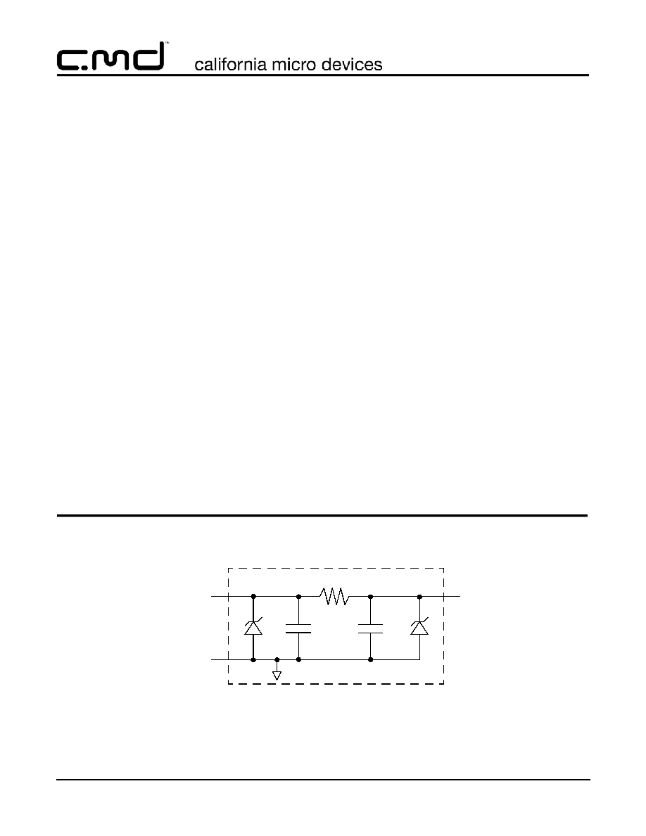
The CM1409 is a family of pi-style EMI filter arrays with
ESD protection, which integrates six and eight filters
(C-R-C) in small form factor TDFN 0.50mm pitch pack-
ages. The CM1409 has component values of 15pF-
100
-15pF per channel. The CM1409 has a cut-off fre-
quency of 110MHz and can be used in applications
with data rates up to 44Mbps. The parts include ESD
diodes on every pin, which provide a very high level of
protection for sensitive electronic components that may
be subjected to electrostatic discharge (ESD). The
ESD protection diodes safely dissipate ESD strikes of
±15kV, well beyond the maximum requirement of the
IEC61000-4-2 international standard. Using the MIL-
STD-883 (Method 3015) specification for Human Body
Model (HBM) ESD, the pins are protected for contact
discharges at greater than
±30kV.
These devices are particularly well-suited for portable
electronics (e.g. wireless handsets, PDAs, notebook
computers) because of their small package and easy-
to-use pin assignments. In particular, the CM1409 is
ideal for EMI filtering and protecting data and control
lines for the I/O data ports, LCD display and camera
interface in mobile handsets.
The CM1409 is housed in space-saving, low-profile 12-
and 16-lead TDFN packages with a 0.50mm pitch and
is available with lead-free finishing.
100
15pF
15pF
FILTER+ESDn*
GND
FILTER+ESDn*
Electrical Schematic
1 of 6 or 8 EMI/RFI + ESD Channels
* See Package/Pinout Diagram
for expanded pin information.
R
C
C
© 2006 California Micro Devices Corp. All rights reserved.
2
490 N. McCarthy Blvd., Milpitas, CA 95035-5112
Tel: 408.263.3214
Fax: 408.263.7846
www.cmd.com
06/16/06
CM1409
PRELIMINARY
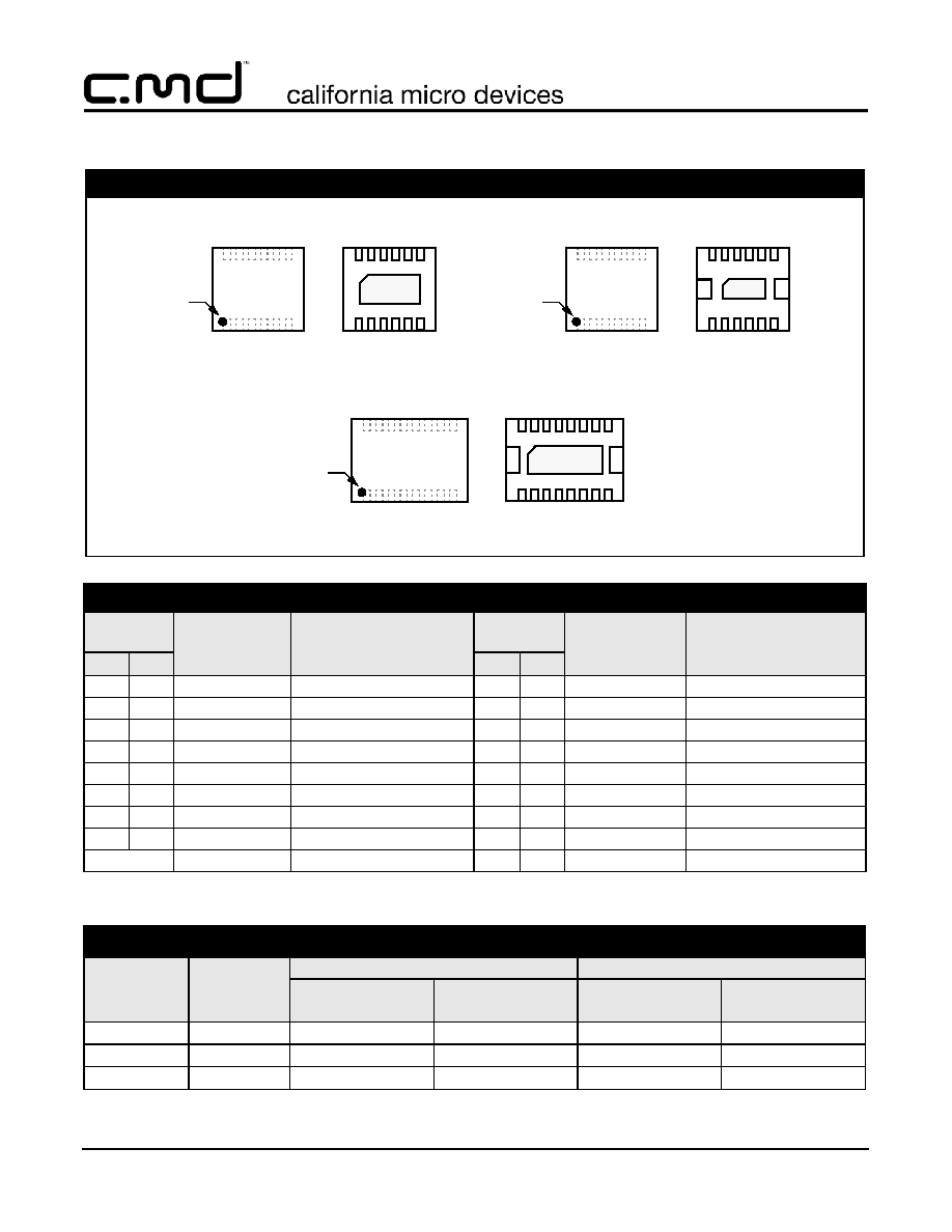
Ordering Information
Note 1: Parts are shipped in Tape & Reel form unless otherwise specified.
PIN DESCRIPTIONS
DEVICE
PIN(s)
NAME
DESCRIPTION
DEVICE
PIN(s)
NAME
DESCRIPTION
-06
-08
-06
-08
1
1
FILTER1
Filter + ESD Channel 1
12
16
FILTER1
Filter + ESD Channel 1
2
2
FILTER2
Filter + ESD Channel 2
11
15
FILTER2
Filter + ESD Channel 2
3
3
FILTER3
Filter + ESD Channel 3
10
14
FILTER3
Filter + ESD Channel 3
4
4
FILTER4
Filter + ESD Channel 4
9
13
FILTER4
Filter + ESD Channel 4
5
5
FILTER5
Filter + ESD Channel 5
8
12
FILTER5
Filter + ESD Channel 5
6
6
FILTER6
Filter + ESD Channel 6
7
11
FILTER6
Filter + ESD Channel 6
7
FILTER7
Filter + ESD Channel 7
10
FILTER7
Filter + ESD Channel 7
8
FILTER8
Filter + ESD Channel 8
9
FILTER8
Filter + ESD Channel 8
GND PAD
GND
Device Ground
PACKAGE / PINOUT DIAGRAMS
Note:
CM1409-06DF/DE
12 Lead TDFN Package
1) These drawings are not to scale.
CM1409-08DF/DE
16 Lead TDFN Package
N09F/E
GND
4
3
2
1
4
3
2
1
8
9
10
11
PAD
9
10
11
12
8
5
5
12
6
7
7
6
4
3
2
1
5 6 7 8
N098F/E
GND
4
3
2
1
12
13
14
15
PAD
13
14
15
16
12
5
16
11
11
6 7
10 9
8
10 9
BOTTOM VIEW
(Pins Up View)
TOP VIEW
(Pins Down View)
BOTTOM VIEW
(Pins Up View)
TOP VIEW
(Pins Down View)
Pin 1
Marking
Pin 1
Marking
CM1409-E6DE
12 Lead TDFN Package
N09EE
GND
4
3
2
1
4
3
2
1
8
9
10
11
PAD
9
10
11
12
8
5
5
12
6
7
7
6
BOTTOM VIEW
(Pins Up View)
TOP VIEW
(Pins Down View)
Pin 1
Marking
PART NUMBERING INFORMATION
Pins
Package
Standard Finish
Lead-free Finish
Ordering Part
Number
1
Part Marking
Ordering Part
Number
1
Part Marking
12
TDFN-12
-
-
CM1409-E6DE
N09EE
12
TDFN-12
CM1409-06DF
N09F
CM1409-06DE
N09E
16
TDFN-16
CM1409-08DF
N098F
CM1409-08DE
N098E

© 2006 California Micro Devices Corp. All rights reserved.
06/16/06
490 N. McCarthy Blvd., Milpitas, CA 95035-5112
Tel: 408.263.3214
Fax: 408.263.7846
www.cmd.com
3
CM1409
PRELIMINARY
Specifications
Note 1: T
A
=25
∞
C unless otherwise specified.
Note 2: ESD applied to input and output pins with respect to GND, one at a time.
Note 3: These parameters are guaranteed by design and characterization.
Note 4: Attenuation / RF curves characterized by a network analyzer using microprobes.
Note 5: These parameters are NOT guaranteed by design, characterization and production.
ABSOLUTE MAXIMUM RATINGS
PARAMETER
RATING
UNITS
Storage Temperature Range
-65 to +150
∞C
DC Power per Resistor
100
mW
DC Package Power Rating
500
mW
STANDARD OPERATING CONDITIONS
PARAMETER
RATING
UNITS
Operating Temperature Range
-40 to +85
∞C
ELECTRICAL OPERATING CHARACTERISTICS
(SEE NOTE1)
SYMBOL
PARAMETER
CONDITIONS
MIN
TYP
MAX
UNITS
R
Resistance
80
100
120
C
TOTAL
Total Channel Capacitance
At 2.5VDC Reverse Bias, 1MHz,
30mVAC
24
30
36
pF
C
Capacitance C
1
At 2.5VDC Reverse Bias, 1MHz,
30mVAC
12
15
18
pF
V
DIODE
Standoff Voltage
I
DIODE
=10
A
6.0
V
I
LEAK
Diode Leakage Current (reverse bias)
V
DIODE
=
+
3.3V
0.1
1.0
A
V
SIG
Signal Clamp Voltage
Positive Clamp
Negative Clamp
I
LOAD
= 10mA
I
LOAD
= -10mA
5.6
-1.5
6.8
-0.8
9.0
-0.4
V
V
V
ESD
In-system ESD Withstand Voltage
a) Human Body Model, MIL-STD-883,
Method 3015
b) Contact Discharge per IEC 61000-4-
2 Level 4
Notes 2 and 3
±30
±15
kV
kV
R
DYN
Dynamic Resistance
Positive
Negative
2.3
0.9
f
C
Cut-off Frequency
Z
SOURCE
=50
, Z
LOAD
=50
Channel R = 100
,
Channel C = 15pF
110
MHz
A
1GHz
Absolute Attenuation @ 1GHz from 0dB
Level
Z
SOURCE
= 50
, Z
LOAD
= 50
,
DC Bias = 0V; Notes 1, 4 and 5
35
dB
A
800MHz -
6GHz
Absolute Attenuation @ 800MHz to
6GHz from 0dB Level
Z
SOURCE
= 50
, Z
LOAD
= 50
,
DC Bias = 0V; Notes 1, 4 and 5
30
dB

© 2006 California Micro Devices Corp. All rights reserved.
4
490 N. McCarthy Blvd., Milpitas, CA 95035-5112
Tel: 408.263.3214
Fax: 408.263.7846
www.cmd.com
06/16/06
CM1409
PRELIMINARY
Performance Information
Typical EMI Filter Performance (T
A
=25∞C, DC Bias=0V, 50 Ohm Environment)
Figure 1. Insertion Loss vs. Frequency (Filter Input to GND)
Typical Diode Capacitance vs. Input Voltage
Figure 2. Filter Capacitance vs. Input Voltage
(normalized to capacitance at 2.5VDC and 25∞C)
C
apacitanc
e
(
Normaliz
ed)
DC Voltage
© 2006 California Micro Devices Corp. All rights reserved.
06/16/06
490 N. McCarthy Blvd., Milpitas, CA 95035-5112
Tel: 408.263.3214
Fax: 408.263.7846
www.cmd.com
5
CM1409
PRELIMINARY
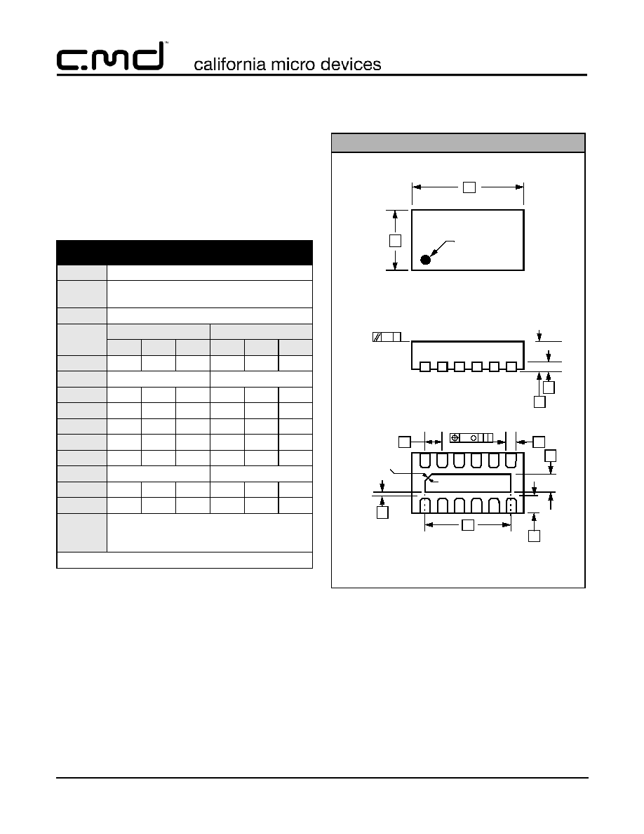
Mechanical Details
TDFN-12 Mechanical Specifications
The CM1409-06DF/DE is supplied in an 12-lead,
0.5mm pitch TDFN package. Dimensions are pre-
sented below.
For complete information on the TDFN-12, see the Cal-
ifornia Micro Devices TDFN Package Information doc-
ument.
This package is compliant with JEDEC standard MO-229C with the
exception of the "D", "D2", "E", "E2", "K" and "L" dimensions as
called out in the table above.
Dimensions for 12-Lead, 0.5mm pitch
TDFN package
PACKAGE DIMENSIONS
Package
TDFN
JEDEC
No.
MO-229C
Leads
12
Dim.
Millimeters
Inches
Min
Nom
Max
Min
Nom
Max
A
0.70
0.75
0.80
0.028 0.030 0.031
A3
0.20 REF
0.008 REF
b
0.20
0.25
0.30
0.008 0.010 0.012
D
2.90
3.00
3.10
0.114 0.118 0.122
D2
2.40
2.50
2.60
0.095 0.098 0.102
E
1.25
1.35
1.45
0.049 0.053 0.057
E2
0.35
0.40
0.45
0.014 0.016 0.018
e
0.50 BSC
0.020 BSC
K
0.20
0.008
L
0.20
0.25
0.30
0.008 0.010 0.012
# per
tape and
reel
3000 pieces
Controlling dimension: millimeters
Mechanical Package Diagrams
BOTTOM VIEW
b
L
0.10
C A B
M
8X
D2
E2
e
GND PAD
K
10
11
12
2
1
3
4
9
Pin 1
C0.2
5
6
8
7
Locator
TOP VIEW
D
E
Pin 1
Marking
4
3
2
1
9
11
12
5
8
6
10
7
A
A3
0.10 C
SIDE VIEW