
© 2005 California Micro Devices Corp. All rights reserved.
08/30/05
490 N. McCarthy Blvd., Milpitas, CA 95035-5112
Tel: 408.263.3214
Fax: 408.263.7846
www.calmicro.com
1
CM1426
PRELIMINARY
LCD and Camera EMI Filter Array with ESD Protection
Features
∑
Four, six and eight channels of EMI filtering with
integrated ESD protection
∑
0.5mm pitch, 10-bump, 1.96mm x 1.33mm foot-
print Chip Scale Package (CM1426-04)
∑
0.5mm pitch, 15-bump, 2.96mm x 1.33mm foot-
print Chip Scale Package (CM1426-06)
∑
0.5mm pitch, 20-bump, 3.96mm x 1.33mm foot-
print Chip Scale Package (CM1426-08)
∑
Pi-style EMI filters in a capacitor-resistor-capacitor
(C-R-C) network
∑
±8kV ESD protection on each channel
(IEC 61000-4-2 Level 4, contact discharge)
∑
±15kV ESD protection on each channel (HBM)
∑
Greater than 20dB attenuation (typical) at 1 GHz
∑
Chip Scale Package features extremely low
lead inductance for optimum filter and ESD
performance
∑
Optiguard
TM
coated for improved reliability at
assembly
∑
Lead-free version available
Applications
∑
LCD and Camera data lines in mobile handsets
∑
I/O port protection for mobile handsets, notebook
computers, PDAs etc.
∑
EMI filtering for data ports in cell phones, PDAs or
notebook computers.
∑
Wireless handsets
∑
Handheld PCs/PDAs
∑
LCD and camera modules
Product Description
The CM1426 is a family of pi-style EMI filter arrays with
ESD protection, which integrates four, six and eight fil-
ters (C-R-C) in a Chip Scale Package with 0.50mm
pad pitch. The CM1426 has component values of
8.5pF-100
-8.5pF per channel. The CM1426 has a
cut-off frequency of 230MHz and can be used in appli-
cations where the data rates are as high as 92Mbps.
The parts include avalanche-type ESD diodes on every
pin, which provide a very high level of protection for
sensitive electronic components that may be subjected
to electrostatic discharge (ESD). The ESD protection
diodes safely dissipate ESD strikes of
±8kV, well
beyond the maximum requirement of the IEC61000-4-
2 international standard. Using the MIL-STD-883
(Method 3015) specification for Human Body Model
(HBM) ESD, the pins are protected for contact dis-
charges at greater than
±15kV.
These devices are particularly well-suited for portable
electronics (e.g. wireless handsets, PDAs, notebook
computers) because of their small package and easy-
to-use pin assignments. In particular, the CM1426 is
ideal for EMI filtering and protecting data and control
lines for the I/O data ports, LCD display and camera
interface in mobile handsets.
The CM1426 incorporates Optiguard
TM
which results in
improved reliability at assembly. The CM1426 is avail-
able in a space-saving, low-profile Chip Scale Package
with optional lead-free finishing.
100
8.5pF
8.5pF
FILTER+ESDn*
GND*
FILTER+ESDn*
Electrical Schematic
1 of 4, 6 or 8 EMI/RFI + ESD Channels
* See Package/Pinout Diagram
for expanded pin information.
(Pins B1-Bm)
(Pins A1-An)
(Pins C1-Cn)
© 2005 California Micro Devices Corp. All rights reserved.
08/30/05
490 N. McCarthy Blvd., Milpitas, CA 95035-5112
Tel: 408.263.3214
Fax: 408.263.7846
www.calmicro.com
3
CM1426
PRELIMINARY
Ordering Information
Note 1: Parts are shipped in Tape & Reel form unless otherwise specified.
Note 2: Lead-free devices are specified by using a "+" character for the top side orientation mark.
Specifications
PART NUMBERING INFORMATION
Bumps
Package
Standard Finish
Lead-free Finish
2
Ordering Part
Number
1
Part Marking
Ordering Part
Number
1
Part Marking
10
CSP
CM1426-04CS
N264
CM1426-04CP
N264
15
CSP
CM1426-06CS
N266
CM1426-06CP
N266
20
CSP
CM1426-08CS
N268
CM1426-08CP
N268
ABSOLUTE MAXIMUM RATINGS
PARAMETER
RATING
UNITS
Storage Temperature Range
-65 to +150
∞C
DC Power per Resistor
100
mW
DC Package Power Rating
500
mW
STANDARD OPERATING CONDITIONS
PARAMETER
RATING
UNITS
Operating Temperature Range
-40 to +85
∞C
ELECTRICAL OPERATING CHARACTERISTICS
(SEE NOTE1)
SYMBOL
PARAMETER
CONDITIONS
MIN
TYP
MAX
UNITS
R
Resistance
80
100
120
C
TOTAL
Total Channel Capacitance
At 2.5VDC Reverse
Bias, 1MHz, 30mVAC
13.6
17
20.4
pF
C
Capacitance C1
At 2.5VDC Reverse
Bias, 1MHz, 30mVAC
6.8
8.5
10.2
pF
V
DIODE
Standoff Voltage
I
DIODE
=10
A
6.0
V
I
LEAK
Diode Leakage Current (reverse bias)
V
DIODE
=
3.3V
0.1
1
A
V
SIG
Signal Clamp Voltage
Positive Clamp
Negative Clamp
I
LOAD
= 10mA
I
LOAD
= -10mA
5.6
-1.5
6.8
-0.8
9.0
-0.4
V
V
V
ESD
In-system ESD Withstand Voltage
a) Human Body Model, MIL-STD-883, Method
3015
b) Contact Discharge per IEC 61000-4-2 Level 4
Notes 2 and 3
±15
±8
kV
kV

© 2005 California Micro Devices Corp. All rights reserved.
4
490 N. McCarthy Blvd., Milpitas, CA 95035-5112
Tel: 408.263.3214
Fax: 408.263.7846
www.calmicro.com
08/30/05
CM1426
PRELIMINARY
Note 1: T
A
=25
∞
C unless otherwise specified.
Note 2: ESD applied to input and output pins with respect to GND, one at a time.
Note 3: These parameters are guaranteed by design and characterization.
R
DYN
Dynamic Resistance
Positive
Negative
2.3
0.9
f
C
Cut-off Frequency
Z
SOURCE
=50
, Z
LOAD
=50
R=100
, C=17pF
230
MHz
ELECTRICAL OPERATING CHARACTERISTICS
(SEE NOTE1)
© 2005 California Micro Devices Corp. All rights reserved.
08/30/05
490 N. McCarthy Blvd., Milpitas, CA 95035-5112
Tel: 408.263.3214
Fax: 408.263.7846
www.calmicro.com
5
CM1426
PRELIMINARY
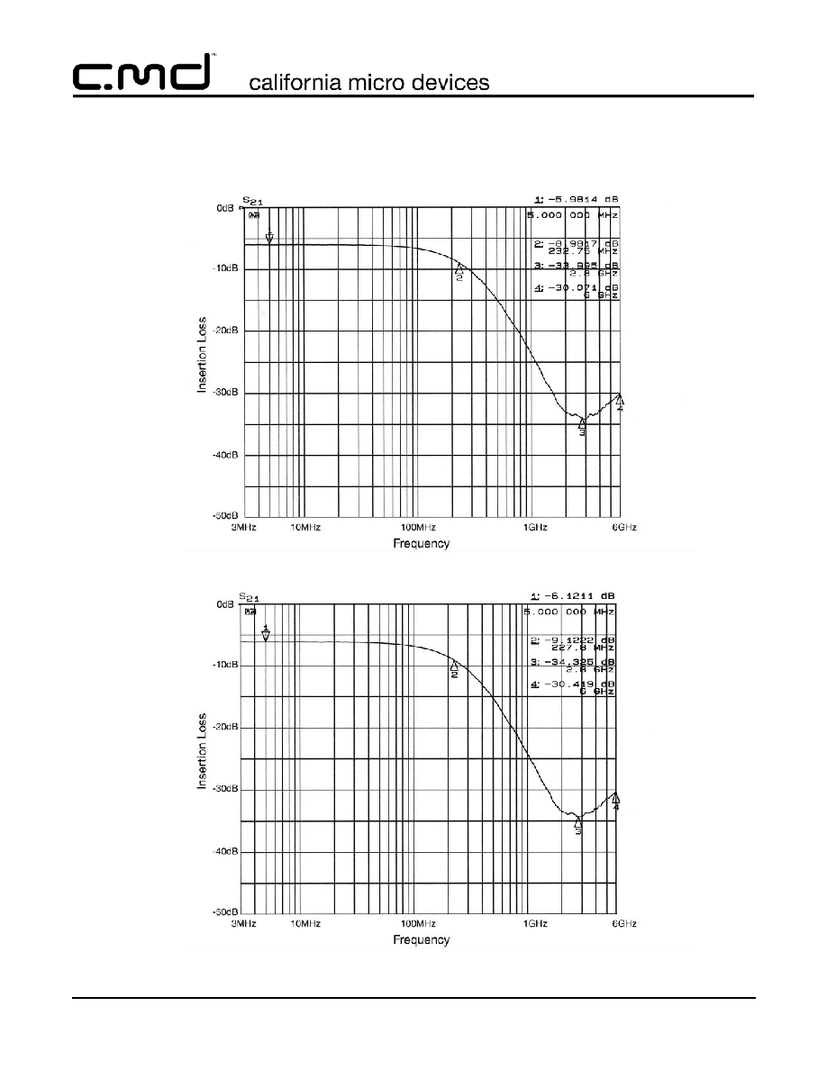
Performance Information
Typical Filter Performance (T
A
=25∞C, DC Bias=0V, 50 Ohm Environment)
Figure 1. Insertion Loss vs. Frequency (A1-C1 to GND B1)
Figure 2. Insertion Loss vs. Frequency (A2-C2 to GND B1)
