 | –≠–ª–µ–∫—Ç—Ä–æ–Ω–Ω—ã–π –∫–æ–º–ø–æ–Ω–µ–Ω—Ç: CM1430 | –°–∫–∞—á–∞—Ç—å:  PDF PDF  ZIP ZIP |
© 2006 California Micro Devices Corp. All rights reserved.
03/02/06
490 N. McCarthy Blvd., Milpitas, CA 95035-5112
Tel: 408.263.3214
Fax: 408.263.7846
www.cmd.com
1
CM1430
LCD and Camera EMI Filter Array with ESD Protection
Features
∑
Four, six and eight channels of EMI filtering with
integrated ESD protection
∑
Pi-style EMI filters in a capacitor-resistor-capacitor
(C-R-C) network
∑
±15kV ESD protection on each channel
(IEC 61000-4-2 Level 4, contact discharge)
∑
±30kV ESD protection on each channel (HBM)
∑
Greater than 20dB attenuation (typical) at 1 GHz
∑
TDFN package with 0.40mm lead pitch:
∑ 4-ch. = 8-lead TDFN
∑ 6-ch. = 12-lead TDFN
∑ 8-ch. = 16-lead TDFN
∑
Tiny TDFN package size:
∑ 8-lead: 1.7mm x 1.35mm
∑ 12-lead: 2.5mm x 1.35mm
∑ 16-lead: 3.3mm x 1.35mm
∑
Increased robustness against vertical impacts
during manufacturing process
∑
Lead-free version available
Applications
∑
LCD and Camera data lines in mobile handsets
∑
I/O port protection for mobile handsets, notebook
computers, PDAs etc.
∑
EMI filtering for data ports in cell phones, PDAs or
notebook computers.
∑
Wireless handsets
∑
Handheld PCs/PDAs
∑
LCD and camera modules
Product Description
The CM1430 is a family of pi-style EMI filter arrays with
ESD protection, which integrates four, six and eight fil-
ters (C-R-C) in small form factor TDFN 0.40mm pitch
packages. The CM1430 has component values of
8.5pF-100
-8.5pF per channel. The CM1430 has a
cut-off frequency of 200MHz and can be used in appli-
cations with data rates up to 80Mbps. The parts
include ESD diodes on every pin, which provide a very
high level of protection for sensitive electronic compo-
nents that may be subjected to electrostatic discharge
(ESD). The ESD protection diodes safely dissipate
ESD strikes of
±15kV, well beyond the maximum
requirement of the IEC61000-4-2 international stan-
dard. Using the MIL-STD-883 (Method 3015) specifica-
tion for Human Body Model (HBM) ESD, the pins are
protected for contact discharges at greater than
±30kV.
These devices are particularly well-suited for portable
electronics (e.g. wireless handsets, PDAs, notebook
computers) because of their small package and easy-
to-use pin assignments. In particular, the CM1430 is
ideal for EMI filtering and protecting data and control
lines for the I/O data ports, LCD display and camera
interface in mobile handsets.
The CM1430 is housed in space-saving, low-profile 8-,
12- and 16-lead TDFN packages with a 0.4mm pitch
and is available with lead-free finishing. This new
small TDFN package provides up to 42% board space
savings vs. the 0.50mm pitch TDFN packages.
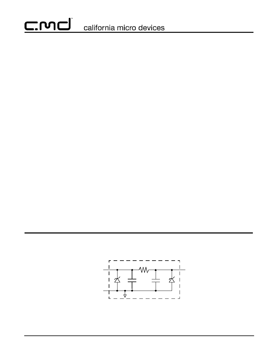
100
8.5pF
8.5pF
FILTER+ESDn*
GND
FILTER+ESDn*
Electrical Schematic
1 of 4, 6 or 8 EMI/RFI Filter Channels
* See Package/Pinout Diagram
for expanded pin information.
with Integrated ESD Protection
© 2006 California Micro Devices Corp. All rights reserved.
2
490 N. McCarthy Blvd., Milpitas, CA 95035-5112
Tel: 408.263.3214
Fax: 408.263.7846
www.cmd.com
03/02/06
CM1430
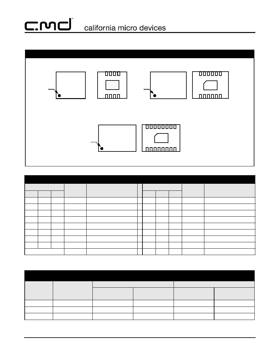
Ordering Information
Note 1: Parts are shipped in Tape & Reel form unless otherwise specified.
PIN DESCRIPTIONS
DEVICE PIN(s)
NAME
DESCRIPTION
DEVICE PIN(s)
NAME
DESCRIPTION
-04
-06
-08
-04
-06
-08
1
1
1
FILTER1 Filter + ESD Channel 1
8
12
16
FILTER1 Filter + ESD Channel 1
2
2
2
FILTER2 Filter + ESD Channel 2
7
11
15
FILTER2 Filter + ESD Channel 2
3
3
3
FILTER3 Filter + ESD Channel 3
6
10
14
FILTER3 Filter + ESD Channel 3
4
4
4
FILTER4 Filter + ESD Channel 4
5
9
13
FILTER4 Filter + ESD Channel 4
5
5
FILTER5 Filter + ESD Channel 5
8
12
FILTER5 Filter + ESD Channel 5
6
6
FILTER6 Filter + ESD Channel 6
7
11
FILTER6 Filter + ESD Channel 6
7
FILTER7 Filter + ESD Channel 7
10
FILTER7 Filter + ESD Channel 7
8
FILTER8 Filter + ESD Channel 8
9
FILTER8 Filter + ESD Channel 8
GND PAD
GND
Device Ground
PACKAGE / PINOUT DIAGRAMS
Notes:
BOTTOM VIEW
CM1430-06DF/DE
12 Lead TDFN Package
(Pins Up View)
TOP VIEW
(Pins Down View)
1) These drawings are not to scale.
CM1430-08DF/DE
16 Lead TDFN Package
CM1430-04DF/DE
8 Lead TDFN Package
GND
PAD
XXXX
GND
4
3
2
1
4
3
2
1
8
9
10
11
PAD
9
10
11
12
8
5
5
12
6
7
7
6
4
3
2
1
5 6 7 8
XXXXX
GND
4
3
2
1
12
13
14
15
PAD
13
14
15
16
12
5
16
11
11
6 7
10 9
8
10 9
4
3
2
1
5
6
7
8
BOTTOM VIEW
(Pins Up View)
TOP VIEW
(Pins Down View)
BOTTOM VIEW
(Pins Up View)
TOP VIEW
(Pins Down View)
Pin 1
XX
4
3
2
1
5
6
7
8
Marking
Pin 1
Marking
Pin 1
Marking
PART NUMBERING INFORMATION
Pins
Package
Standard Finish
Lead-free Finish
Ordering Part
Number
1
Part Marking
Ordering Part
Number
1
Part Marking
8
TDFN-8
CM1430-04DF
VF
CM1430-04DE
VE
12
TDFN-12
CM1430-06DF
N30F
CM1430-06DE
N30E
16
TDFN-16
CM1430-08DF
N308F
CM1430-08DE
N308E
© 2006 California Micro Devices Corp. All rights reserved.
03/02/06
490 N. McCarthy Blvd., Milpitas, CA 95035-5112
Tel: 408.263.3214
Fax: 408.263.7846
www.cmd.com
3
CM1430
Specifications
Note 1: T
A
=25
∞
C unless otherwise specified.
Note 2: ESD applied to input and output pins with respect to GND, one at a time.
Note 3: These parameters are guaranteed by design and characterization.
ABSOLUTE MAXIMUM RATINGS
PARAMETER
RATING
UNITS
Storage Temperature Range
-65 to +150
∞C
DC Power per Resistor
100
mW
DC Package Power Rating
500
mW
STANDARD OPERATING CONDITIONS
PARAMETER
RATING
UNITS
Operating Temperature Range
-40 to +85
∞C
ELECTRICAL OPERATING CHARACTERISTICS
(SEE NOTE1)
SYMBOL
PARAMETER
CONDITIONS
MIN
TYP
MAX
UNITS
R
Resistance
80
100
120
C
TOTAL
Total Channel Capacitance
At 2.5VDC Reverse
Bias, 1MHz, 30mVAC
14
17
22
pF
C
Capacitance C1
At 2.5VDC Reverse
Bias, 1MHz, 30mVAC
7
8.5
11
pF
V
DIODE
Standoff Voltage
I
DIODE
=10
A
6.0
V
I
LEAK
Diode Leakage Current (reverse bias)
V
DIODE
=+3.3V
0.1
1.0
A
V
SIG
Signal Clamp Voltage
Positive Clamp
Negative Clamp
I
LOAD
= 10mA
I
LOAD
= -10mA
5.6
-1.5
6.8
-0.8
9.0
-0.4
V
V
V
ESD
In-system ESD Withstand Voltage
a) Human Body Model, MIL-STD-883, Method
3015
b) Contact Discharge per IEC 61000-4-2 Level 4
Notes 2 and 3
±30
±15
kV
kV
R
DYN
Dynamic Resistance
Positive
Negative
2.3
0.9
f
C
Cut-off Frequency
Z
SOURCE
=50
, Z
LOAD
=50
Channel R = 100
,
Channel C = 8.5pF
200
MHz
© 2006 California Micro Devices Corp. All rights reserved.
4
490 N. McCarthy Blvd., Milpitas, CA 95035-5112
Tel: 408.263.3214
Fax: 408.263.7846
www.cmd.com
03/02/06
CM1430
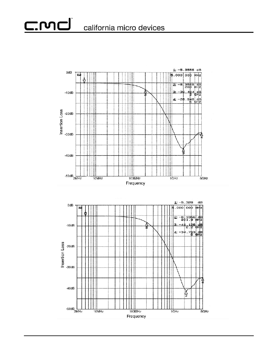
Performance Information
Typical Filter Performance (T
A
=25∞C, DC Bias=0V, 50 Ohm Environment)
Figure 1. Insertion Loss vs. Frequency (FILTER1 Input to GND)
Figure 2. Insertion Loss vs. Frequency (FILTER2 Input to GND)

© 2006 California Micro Devices Corp. All rights reserved.
03/02/06
490 N. McCarthy Blvd., Milpitas, CA 95035-5112
Tel: 408.263.3214
Fax: 408.263.7846
www.cmd.com
5
CM1430
Performance Information (cont'd)
Typical Filter Performance (T
A
=25∞C, DC Bias=0V, 50 Ohm Environment)
Figure 3. Insertion Loss vs. Frequency (FILTER3 Input to GND)
Figure 4. Insertion Loss vs. Frequency (FILTER4 Input to GND)
© 2006 California Micro Devices Corp. All rights reserved.
6
490 N. McCarthy Blvd., Milpitas, CA 95035-5112
Tel: 408.263.3214
Fax: 408.263.7846
www.cmd.com
03/02/06
CM1430
Performance Information (cont'd)
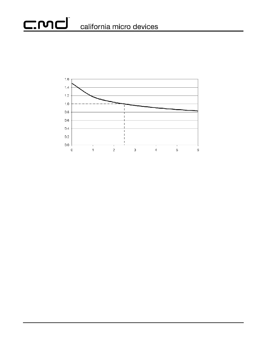
Typical Diode Capacitance vs. Input Voltage
Figure 5. Filter Capacitance vs. Input Voltage
(normalized to capacitance at 2.5VDC and 25∞C)
C
apacitanc
e
(
Normaliz
ed)
DC Voltage

© 2006 California Micro Devices Corp. All rights reserved.
03/02/06
490 N. McCarthy Blvd., Milpitas, CA 95035-5112
Tel: 408.263.3214
Fax: 408.263.7846
www.cmd.com
7
CM1430
Mechanical Details
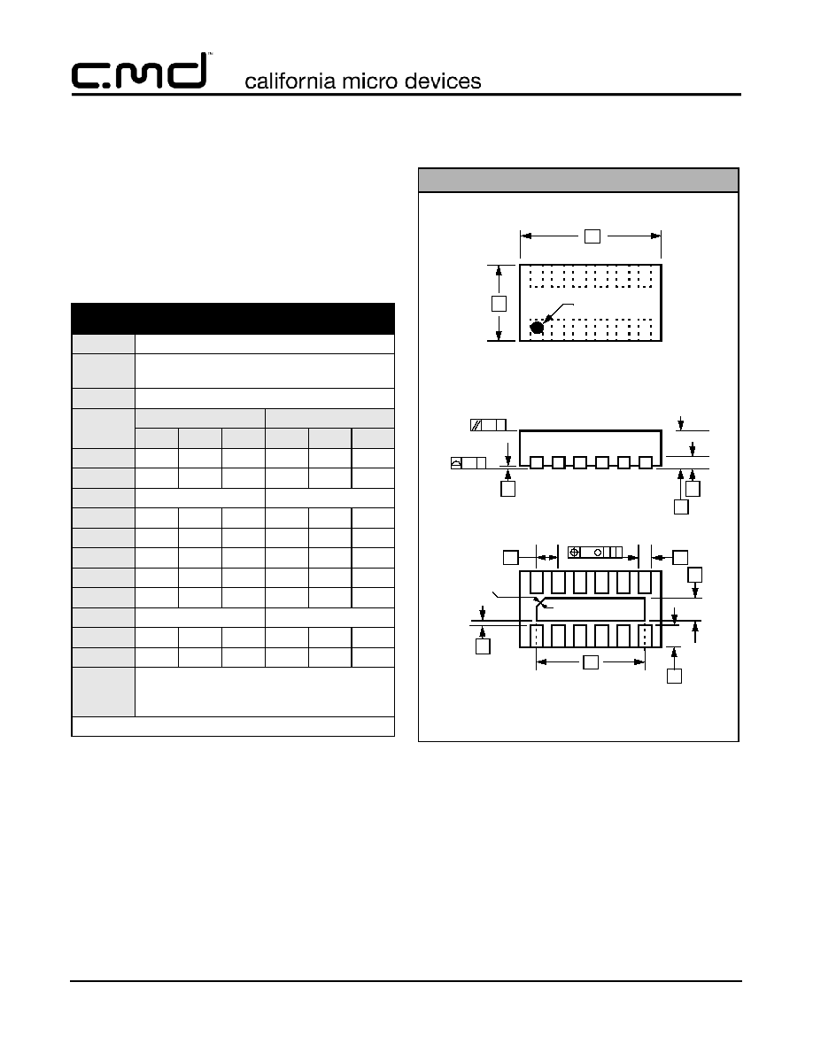
CM1430-04DF/DE Mechanical Specifications
Dimensions for the CM1430-04DF/DE suplied in a 8-
lead, 0.4mm pitch TDFN package are presented
below.
For complete information on the TDFN-8, see the Cali-
fornia Micro Devices TDFN Package Information docu-
ment.
This package is compliant with JEDEC standard MO-229C with the
exception of the "D", "D2", "E", "E2", "K" and "L" dimensions as
called out in the table above.
Dimensions for 8-Lead, 0.4mm pitch
TDFN package
PACKAGE DIMENSIONS
Package
TDFN
JEDEC
No.
MO-229C
Leads
8
Dim.
Millimeters
Inches
Min
Nom
Max
Min
Nom
Max
A
0.70
0.75
0.80
0.028 0.030 0.031
A1
0.00
0.02
0.05
0.000 0.001 0.002
A3
0.20 REF
0.008 REF
b
0.15
0.20
0.25
0.006 0.008 0.010
D
1.60
1.70
1.80
0.063 0.067 0.071
D2
1.10
1.20
1.30
0.043 0.047 0.051
E
1.25
1.35
1.45
0.049 0.053 0.057
E2
0.30
0.40
0.50
0.012 0.016 0.020
e
0.40 BSC
0.016 BSC
K
0.20
0.008
L
0.15
0.25
0.35
0.006 0.010 0.014
# per
tape and
reel
3000 pieces
Controlling dimension: millimeters
Mechanical Package Diagrams
BOTTOM VIEW
b
L
0.10
C A B
M
8X
D2
E2
e
GND
K
7
8
1
2
3
6
Pin 1
C0.2
4
5
Locator
TOP VIEW
D
E
Pin 1
Marking
4
3
2
1
5
7
8
6
PAD
A
A3
A1
0.10 C
0.08 C
SIDE VIEW
© 2006 California Micro Devices Corp. All rights reserved.
8
490 N. McCarthy Blvd., Milpitas, CA 95035-5112
Tel: 408.263.3214
Fax: 408.263.7846
www.cmd.com
03/02/06
CM1430
Mechanical Details (cont'd)
CM1430-06DF/DE Mechanical Specifications
Dimensions for the CM1430-06DF/DE suplied in a 12-
lead, 0.4mm pitch TDFN package are presented
below.
For complete information on the TDFN-12, see the Cal-
ifornia Micro Devices TDFN Package Information doc-
ument.
This package is compliant with JEDEC standard MO-229C with the
exception of the "D", "D2", "E", "E2", "K" and "L" dimensions as
called out in the table above.
Dimensions for 12-Lead, 0.4mm pitch
TDFN package
PACKAGE DIMENSIONS
Package
TDFN
JEDEC
No.
MO-229C
Leads
12
Dim.
Millimeters
Inches
Min
Nom
Max
Min
Nom
Max
A
0.70
0.75
0.80
0.028 0.030 0.031
A1
0.00
0.02
0.05
0.000 0.001 0.002
A3
0.20 REF
0.008 REF
b
0.15
0.20
0.25
0.006 0.008 0.010
D
2.40
2.50
2.60
0.094 0.098 0.102
D2
1.90
2.00
2.10
0.075 0.079 0.083
E
1.25
1.35
1.45
0.049 0.053 0.057
E2
0.30
0.40
0.50
0.012 0.016 0.020
e
0.40 BSC
0.016 BSC
K
0.20
0.008
L
0.15
0.25
0.35
0.006 0.010 0.014
# per
tape and
reel
3000 pieces
Controlling dimension: millimeters
Mechanical Package Diagrams
BOTTOM VIEW
b
L
0.10
C A B
M
8X
D2
E2
e
GND PAD
K
10
11
12
2
1
3
4
9
Pin 1
C0.1
5
6
8
7
Locator
TOP VIEW
D
E
Pin 1
Marking
4
3
2
1
9
11
12
5
8
6
10
7
A
A3
A1
0.10 C
0.08 C
SIDE VIEW

© 2006 California Micro Devices Corp. All rights reserved.
03/02/06
490 N. McCarthy Blvd., Milpitas, CA 95035-5112
Tel: 408.263.3214
Fax: 408.263.7846
www.cmd.com
9
CM1430
Mechanical Details (cont'd)
CM1430-08DF/DE Mechanical Specifications
Dimensions for the CM1430-08DF/DE supplied in a
16-lead, 0.4mm pitch TDFN package are presented
below.
For complete information on the TDFN-16, see the Cal-
ifornia Micro Devices TDFN Package Information doc-
ument.
This package is compliant with JEDEC standard MO-229C with the
exception of the "D", "D2", "E", "E2", "K" and "L" dimensions as
called out in the table above.
Dimensions for 16-Lead, 0.4mm pitch
TDFN package
PACKAGE DIMENSIONS
Package
TDFN
JEDEC
No.
MO-229C
Leads
16
Dim.
Millimeters
Inches
Min
Nom
Max
Min
Nom
Max
A
0.70
0.75
0.80
0.028 0.030 0.031
A1
0.00
0.02
0.05
0.000 0.001 0.002
A3
0.200 REF
0.008 REF
b
0.15
0.20
0.25
0.006 0.008 0.010
D
3.20
3.30
3.40
0.126 0.130 0.134
D2
2.70
2.80
2.90
0.106 0.110 0.114
E
1.25
1.35
1.45
0.049 0.053 0.057
E2
0.30
0.40
0.50
0.012 0.016 0.020
e
0.40 BSC
0.016 BSC
K
0.20
0.008
L
0.15
0.25
0.35
0.006 0.010 0.014
# per
tape and
reel
3000 pieces
Controlling dimension: millimeters
Mechanical Package Diagrams
BOTTOM VIEW
A
A3
A1
0.10 C
0.08 C
SIDE VIEW
b
L
0.10
C A B
M
8X
D2
E2
e
GND PAD
K
13
14
15
16
3
2
1
4
5
12
Pin 1
C0.2
6
7
8
11 10
9
Locator
TOP VIEW
D
E
Pin 1
Marking
4
3
2
1
13
15
16
5
12
8
7
6
14
9
11 10