©
2005 California Micro Devices Corp. All rights reserved.
01/27/05
430 N. McCarthy Blvd., Milpitas, CA 95035-5112
Tel: 408.263.3214
Fax: 408.263.7846
www.calmicro.com
1
CM1450
PRELIMINARY
LCD & Camera EMI Filter Array with ESD Protection
Features
∑
Six and eight channels of EMI filtering
∑
Utilizes Praetorian
TM inductor-based design tech-
nology for true L-C filter implementation
∑
OptiGuard
TM coating for improved reliability
∑
±15kV ESD protection on each channel
(IEC 61000-4-2 Level 4, contact discharge)
∑
±30kV ESD protection on each channel (HBM)
∑
Better than 40dB of attenuation at 1GHz
∑
Chip Scale Package features extremely low
lead inductance for optimum filter and ESD
performance
∑
15-bump, 2.960mm x 1.330mm footprint
Chip Scale Package (CM1450-06CS/CP)
∑
20-bump, 4.000mm x 1.458mm footprint
Chip Scale Package (CM1450-08CS/CP)
∑
Lead-free version available
Applications
∑
LCD and Camera data lines in mobile handsets
∑
I/O port protection for mobile handsets, notebook
computers, PDAs, etc.
∑
EMI filtering for data phones in cell phones, PDAs
or notebook computersWireless handsets / cell
phones
∑
Wireless Handsets
∑
Handheld PCs/PDAs
∑
LCD and camera modules
Product Description
The CM1450 comprises a family of inductor-capacitor
(L-C) based EMI filter arrays with integrated ESD pro-
tection in CSP form factor. The CM1450-06 and
CM1450-08 are configured in 6 and 8 channel formats
respectively. Each EMI filter channel of the CM1450 is
implemented as a 5-pole L-C filter where the compo-
nent values are 15pF-17nH-15pF-17nF-15pF. The
CM1450's roll-off frequency at -10dB attenuation is
300MHz and can be used in applications where the
data rates are as high as 120Mbps while providing
greater than 35dB over the 800MHz to 2.7GHz fre-
quency range. The parts integrate ESD protection
diodes on every pin, which provide a very high level of
protection for sensitive electronic components that may
be subjected to electrostatic discharge (ESD). The
ESD protection diodes connected to the filter ports are
designed and characterized to safely dissipate ESD
strikes of
±15kV, beyond the Level 4 requirement of
the IEC61000-4-2 international standard. Using the
MIL-STD-883 (Method 3015) specification for Human
Body Model (HBM) ESD, the pins are protected for
contact discharges at greater than
±30kV.
This device is particularly well suited for portable elec-
tronics (e.g. wireless handsets, PDAs) because of its
small package format and easy-to-use pin assign-
ments. In particular, the CM1450 is ideal for EMI filter-
ing and protecting data and control lines for the LCD
display and camera interface in wireless handsets.
The CM1450 incorporates OptiGuard
TM which results in
improved reliability at assembly. The CM1450 is avail-
able in a space saving, low profile Chip Scale Package
with optional lead-free finishing.
.
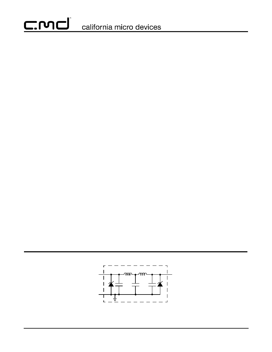
Electrical Schematic
* See Package/Pinout Diagram
1 of n EMI Filtering + ESD Channels
(n = 6 for CM1450-06, 8 for CM1450-08)
for expanded pin information.
L1
C
C
FILTERn*
GND
FILTERn*
(Pins B1-Bn)
C
L2
©
2005 California Micro Devices Corp. All rights reserved.
2
430 N. McCarthy Blvd., Milpitas, CA 95035-5112
Tel: 408.263.3214
Fax: 408.263.7846
www.calmicro.com
01/27/05
CM1450
PRELIMINARY
Ordering Information
Note 1: Parts are shipped in Tape & Reel form unless otherwise specified.
Note 2: Lead-free devices are specified by using a "
+
" character for the top side orientation mark.
FILTER5
FILTER6
GND
FILTER5
FILTER6
A6
A5
Orientation
Marking
B3
C6
C5
FILTER7
FILTER8
GND
FILTER7
FILTER8
A8
A7
B4
C8
C7
FILTER3
FILTER4
GND
FILTER3
FILTER4
A4
A3
B2
C4
C3
FILTER1
FILTER2
GND
FILTER1
FILTER2
A2
A1
B1
C2
C1
A1
N508
4
3
2
6
7
8
5
1
C
B
A
Orientation
Marking
(see note 2)
N506
4
3
2
6
5
1
C
B
A
Orientation
Marking
(see note 2)
FILTER5
FILTER6
GND
FILTER5
FILTER6
A6
A5
Orientation
Marking
B3
C6
C5
FILTER3
FILTER4
GND
FILTER3
FILTER4
A4
A3
B2
C4
C3
FILTER1
FILTER2
GND
FILTER1
FILTER2
A2
A1
B1
C2
C1
A1
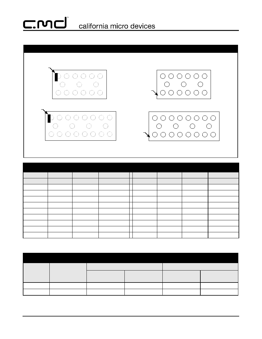
PACKAGE / PINOUT DIAGRAMS
Notes:
BOTTOM VIEW
CM1450-06CS/CP 15-Bump CSP Package
(Bumps Up View)
TOP VIEW
(Bumps Down View)
CM1450 -08CS/CP 20-Bump CSP Package
1) These drawings are not to scale.
2) Lead-free devices are specified by using a "+" character for the top side orientation mark.
PIN DESCRIPTIONS
CM1450
CM1450
NAME
DESCRIPTION
CM1450
CM1450
NAME
DESCRIPTION
PIN(s)
PIN(s)
NAME
DESCRIPTION
PIN(s)
PIN(s)
NAME
DESCRIPTION
A1
A1
FILTER1
Filter Channel 1
C1
C1
FILTER1
Filter Channel 1
A2
A2
FILTER2
Filter Channel 2
C2
C2
FILTER2
Filter Channel 2
A3
A3
FILTER3
Filter Channel 3
C3
C3
FILTER3
Filter Channel 3
A4
A4
FILTER4
Filter Channel 4
C4
C4
FILTER4
Filter Channel 4
A5
A5
FILTER5
Filter Channel 5
C5
C5
FILTER5
Filter Channel 5
A6
A6
FILTER6
Filter Channel 6
C6
C6
FILTER6
Filter Channel 6
-
A7
FILTER7
Filter Channel 7
-
C7
FILTER7
Filter Channel 7
-
A8
FILTER8
Filter Channel 8
-
C8
FILTER8
Filter Channel 8
B1-B3
B1-B4
GND
Device Ground
PART NUMBERING INFORMATION
Bumps
Package
Standard Finish
Lead-free Finish
2
Ordering Part
Number
1
Part Marking
Ordering Part
Number
1
Part Marking
15
CSP
CM1450-06CS
N506
CM1450-06CP
N506
20
CSP
CM1450-08CS
N508
CM1450-08CP
N508

©
2005 California Micro Devices Corp. All rights reserved.
01/27/05
430 N. McCarthy Blvd., Milpitas, CA 95035-5112
Tel: 408.263.3214
Fax: 408.263.7846
www.calmicro.com
3
CM1450
PRELIMINARY
Specifications
Note 1: T
A
=25
∞
C unless otherwise specified.
Note 2: ESD applied to input and output pins with respect to GND, one at a time.
Note 3: Clamping voltage is measured at the opposite side of the EMI filter to the ESD pin. For example, if ESD is applied to Pin A1,
then clamping voltage is measured at Pin C1.
Note 4: Unused pins are left open
Note 5: These parameters are guaranteed by design and characterization.
ABSOLUTE MAXIMUM RATINGS
PARAMETER
RATING
UNITS
Storage Temperature Range
-65 to +150
∞C
DC Power per Resistor
100
mW
DC Package Power Rating
500
mW
STANDARD OPERATING CONDITIONS
PARAMETER
RATING
UNITS
Operating Temperature Range
-40 to +85
∞C
ELECTRICAL OPERATING CHARACTERISTICS
(NOTE 1)
SYMBOL
PARAMETER
CONDITIONS
MIN
TYP
MAX
UNITS
L
TOT
Total Channel Inductance (L
1
+ L
2
)
34
nH
L
1
, L
2
Inductance
17
nH
C
TOT
Total Channel Capcitance (C
1
C
2
C
3
)
At 2.5V DC, 1MHz,
30mV AC
36
45
54
pF
C
1
, C
2
, C
3
Capacitance
At 2.5V DC, 1MHz,
30mV AC
12
15
18
pF
f
C
Cut-off Frequency
Z
SOURCE
=50
, Z
LOAD
=50
137
MHz
f
C
Roll-off Frequency at -10dB Attenuation
Z
SOURCE
=50
, Z
LOAD
=50
300
MHz
V
DIODE
Diode Standoff Voltage
I
DIODE
=10
µA
5.5
V
I
LEAK
Diode Leakage Current (reverse bias)
V
DIODE
=+3.3V
100
nA
V
SIG
Signal Voltage
Positive Clamp
Negative Clamp
I
LOAD
= 10mA
5.6
-1.5
6.8
-0.8
9.0
-0.4
V
V
V
ESD
In-system ESD Withstand Voltage
a) Human Body Model, MIL-STD-883,
Method 3015
b) Contact Discharge per IEC 61000-4-2
Level 4
Notes 2,4 and 5
±30
±15
kV
kV
V
CL
Clamping Voltage during ESD Discharge
MIL-STD-883 (Method 3015), 8kV
Positive Transients
Negative Transients
Notes 2,3,4 and 5
+12
-7
V
V
©
2005 California Micro Devices Corp. All rights reserved.
4
430 N. McCarthy Blvd., Milpitas, CA 95035-5112
Tel: 408.263.3214
Fax: 408.263.7846
www.calmicro.com
01/27/05
CM1450
PRELIMINARY
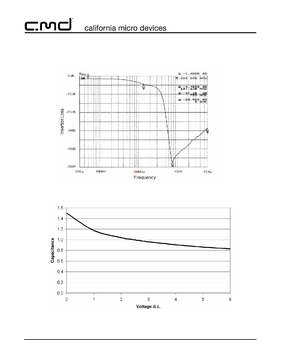
Performance Information
Typical Filter Performance (T
A
=25∞C, DC Bias=0V, 50 Ohm Environment)
Figure 1. Insertion Loss VS. Frequency (A1-C1 to GND B1)
Figure 2. Filter Capacitance vs. Input Voltage over Temperature
(normalized to capacitance at 2.5VDC and 25∞C)
©
2005 California Micro Devices Corp. All rights reserved.
01/27/05
430 N. McCarthy Blvd., Milpitas, CA 95035-5112
Tel: 408.263.3214
Fax: 408.263.7846
www.calmicro.com
5
CM1450
PRELIMINARY
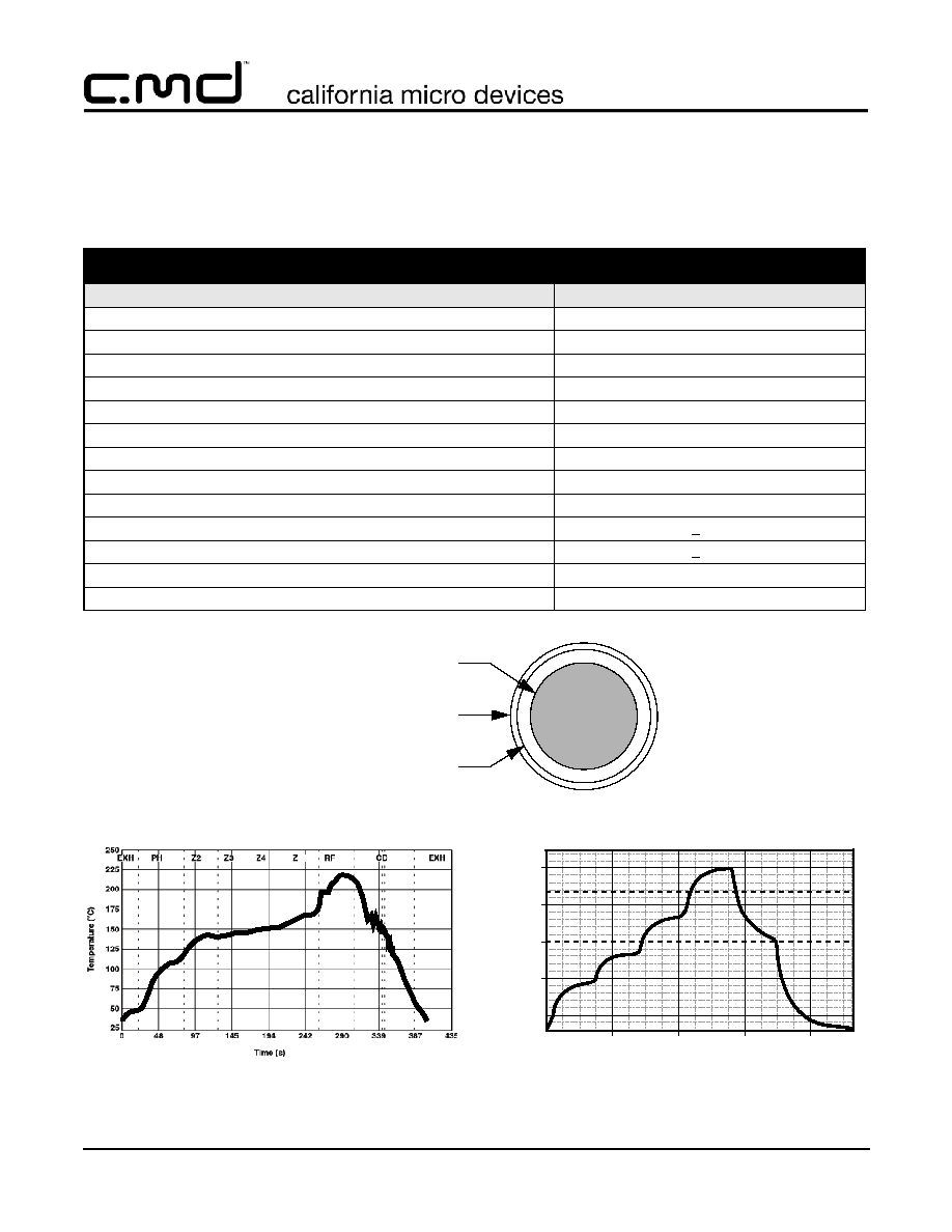
Application Information
Refer to Application Note AP-217, "The Chip Scale
Package", for a detailed description of Chip Scale
Packages offered by California Micro Devices.
Figure 3. Recommended Non-Solder Mask Defined Pad Illustration
Figure 4. Eutectic (SnPb) Solder
Ball Reflow Profile
Figure 5. Lead-free (SnAgCu) Solder
Ball Reflow Profile
PRINTED CIRCUIT BOARD RECOMMENDATIONS
PARAMETER
VALUE
Pad Size on PCB
0.275mm
Pad Shape
Round
Pad Definition
Non-Solder Mask defined pads
Solder Mask Opening
0.325mm Round
Solder Stencil Thickness
0.125mm - 0.150mm
Solder Stencil Aperture Opening (laser cut, 5% tapered walls)
0.330mm Round
Solder Flux Ratio
50/50 by volume
Solder Paste Type
No Clean
Pad Protective Finish
OSP (Entek Cu Plus 106A)
Tolerance -- Edge To Corner Ball
+50
µm
Solder Ball Side Coplanarity
+20
µm
Maximum Dwell Time Above Liquidous
(183∞C)
60 seconds
Soldering Maximum Temperature
260∞C
Solder Mask Opening
0.325mm DIA.
Non-Solder Mask Defined Pad
0.275mm DIA.
Solder Stencil Opening
0.330mm DIA.
200
250
150
100
50
0
1:00.0
2:00.0
3:00.0
4:00.0
Time (minutes)
T
emperature
(∞
C)
©
2005 California Micro Devices Corp. All rights reserved.
6
430 N. McCarthy Blvd., Milpitas, CA 95035-5112
Tel: 408.263.3214
Fax: 408.263.7846
www.calmicro.com
01/27/05
CM1450
PRELIMINARY
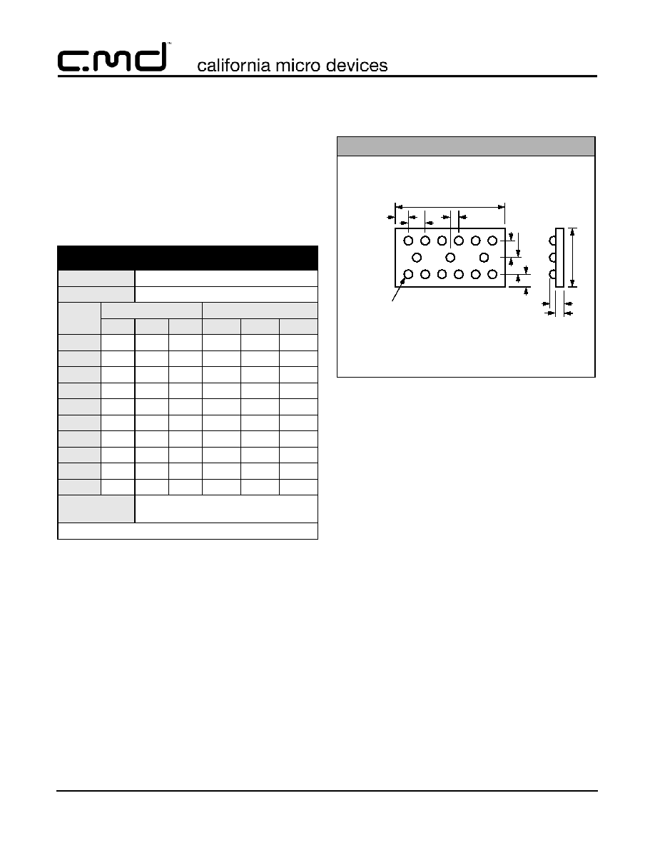
Mechanical Details
CM1450 devices are supplied in custom Chip Scale
Packages (CSP). Dimensions for each of these
devices are presented in the following pages.
CM1450-06CS/CP Mechanical Specifications
The package dimensions for the CM1450-06CS/CP
are presented below.
Package Dimensions for
CM1450-06CS/CP Chip Scale Package
PACKAGE DIMENSIONS
Package
Custom CSP
Bumps
15
Dim
Millimeters
Inches
Min
Nom
Max
Min
Nom
Max
A1
2.915 2.960 3.005 0.1148 0.1165 0.1183
A2
1.285 1.330 1.375 0.0506 0.0524 0.0541
B1
0.495 0.500 0.505 0.0195 0.0197 0.0199
B2
0.245 0.250 0.255 0.0096 0.0098 0.0100
B3
0.430 0.435 0.440 0.0169 0.0171 0.0173
B4
0.430 0.435 0.440 0.0169 0.0171 0.0173
C1
0.180 0.230 0.280 0.0071 0.0091 0.0110
C2
0.180 0.230 0.280 0.0071 0.0091 0.0110
D1
0.561 0.605 0.649 0.0221 0.0238 0.0255
D2
0.355 0.380 0.405 0.0140 0.0150 0.0159
# per tape and
reel
3500 pieces
Controlling dimension: millimeters
Mechanical Package Diagrams
A
B
C
3
4
5
6
C1
B1
A1
B3
C2
DIMENSIONS IN MILLIMETERS
D1
D2
A2
BOTTOM VIEW
SIDE
VIEW
1
2
B2
B4
0.30 DIA.
63/37 Sn/Pb (Eutectic) or
SOLDER BUMPS
96.8/2.6/0.6 Sn/Ag/Cu (Lead-free)
©
2005 California Micro Devices Corp. All rights reserved.
01/27/05
430 N. McCarthy Blvd., Milpitas, CA 95035-5112
Tel: 408.263.3214
Fax: 408.263.7846
www.calmicro.com
7
CM1450
PRELIMINARY
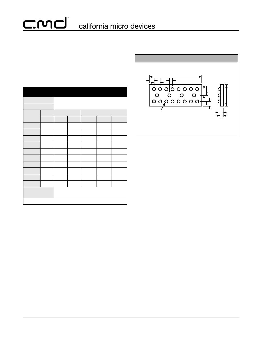
Mechanical Details (cont'd)
CM1450-08CS/CP Mechanical Specifications
The package dimensions for the CM1450-08CS/CP
are presented below.
Package Dimensions for
CM1450-08CS/CP Chip Scale Package
PACKAGE DIMENSIONS
Package
Custom CSP
Bumps
20
Dim
Millimeters
Inches
Min
Nom
Max
Min
Nom
Max
A1
3.955 4.000 4.045 0.1557 0.1575 0.1593
A2
1.413 1.458 1.503 0.0556 0.0574 0.0592
B1
0.495 0.500 0.505 0.0195 0.0197 0.0199
B2
0.245 0.250 0.255 0.0096 0.0098 0.0100
B3
0.430 0.435 0.440 0.0169 0.0171 0.0173
B4
0.430 0.435 0.440 0.0169 0.0171 0.0173
C1
0.200 0.250 0.300 0.0079 0.0098 0.0118
C2
0.244 0.294 0.344 0.0096 0.0116 0.0135
D1
0.561 0.605 0.649 0.0221 0.0238 0.0255
D2
0.355 0.380 0.405 0.0140 0.0150 0.0159
# per tape and
reel
3500 pieces
Controlling dimension: millimeters
Mechanical Package Diagrams
A
C
3
4
5
6
C1
B1
A1
B3
C2
DIMENSIONS IN MILLIMETERS
D1
D2
A2
BOTTOM VIEW
SIDE
VIEW
1
2
B2
B4
7
8
B
A
0.30 DIA.
63/37 Sn/Pb (Eutectic) or
SOLDER BUMPS
96.8/2.6/0.6 Sn/Ag/Cu (Lead-free)
©
2005 California Micro Devices Corp. All rights reserved.
8
430 N. McCarthy Blvd., Milpitas, CA 95035-5112
Tel: 408.263.3214
Fax: 408.263.7846
www.calmicro.com
01/27/05
CM1450
PRELIMINARY
Mechanical Details (cont'd)
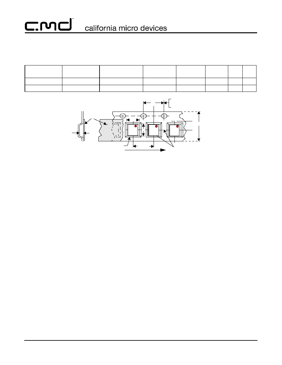
CSP Tape and Reel Specifications
Figure 6. Tape and Reel Mechanical Data
PART NUMBER
CHIP SIZE (mm)
POCKET SIZE (mm)
B
0
X A
0
X K
0
TAPE WIDTH
W
REEL
DIAMETER
QTY PER
REEL
P
0
P
1
CM1450-06
2.96 X 1.33 X 0.6
3.10 X 1.45 X 0.74
8mm
178mm (7")
3500
4mm
4mm
CM1450-08
4.00 X 1.46 X 0.6
4.11 X 1.57 X 0.76
8mm
178mm (7")
3500
4mm
4mm
Top
For Tape Feeder Reference
Cover
Tape
P
1
Only including Draft.
Concentric Around B.
K
o
Embossment
User Direction of Feed
±
0.2 mm
P
o
Center Lines
of Cavity
W
10 Pitches Cumulative
Tolerance On Tape
A
o
B
o