
CALIFORNIA MICRO DEVICES
PACDN005
2/00
1
215 Topaz Street, Milpitas, California 95035 Tel: (408) 263-3214 Fax: (408) 263-7846 www.calmicro.com
©2000 California Micro Devices Corp. All rights reserved.
Features
36 integrated diodes in a single package
offers 18 channel, dual rail clamping action
Provides proper bus termination independent of
external line or card loading conditions
Schottky diode technology; excellent forward
voltage and reverse recovery characteristics
24-pin QSOP package saves board space and
eases layout in space critical bus termination
applications versus discrete approaches
Product Description
Note: CMDs P/Active DN005 Schottky Diode High Speed Bus Terminator is an upgraded version of the original PDN001 or
IPEC DN001 Diode Array. PACDN005 provides minimized lead inductance and parasitic capacitive effects (with added ground
pins), improved forward voltage and crosstalk attributes, and excellent termination performance characteristics at high data
transmission rates. The PACDN005 is recommended for all new designs.
Reflections on high speed data lines lead to undershoot and overshoot disturbances which may result in improper system
operation. Resistor terminations, when used to terminate high speed data lines, increase power consumption and degrade
output (high) levels resulting in reduced noise immunity. Schottky diode termination is the best overall solution for applica-
tions in which power consumption and noise immunity are critical considerations.
CMDs P/Active DN005 Schottky Diode High Speed Bus Terminator
is specifically designed to minimize undershoot/over-
shoot disturbances caused by reflection noise on high speed bus lines such as v2.1 66MHz PCI buses, all varieties of RISC
embedded processor/control local buses, synchronous DRAM, and other high speed memory bus termination applications.
This highly integrated Schottky diode network provides very effective termination performance for high speed data lines under
variable loading conditions. The device supports up to 18 terminated lines per package each of which can be simulta-
neously clamped to both ground and power supply rail. A typical bus termination application will utilize three PAC DN005
devices to replace approximately 50 conventional Schottky diode pairs; thus providing significant reductions in component
and assembly costs, improvements in manufacturing efficiency and reliability, and savings in allocated board area for space-
critical designs.
Applications
PCI v2.1 Bus Termination for Intel-based PentiumÆ
and Pentium Pro systems
Local high speed bus termination for all popular
RISC and embedded microprocessor applications
High speed memory and SDRAM Memory
Bus Termination
P/ACTIVE SCHOTTKY DIODE HIGH SPEED BUS TERMINATOR
Refer to AP-201 Termination Application Note for
further information.
SCHEMATIC CONFIGURATION
24
1
2
3
4
5
6
7
8
9
10
11
12
23
22
21
20
19
18
13
14
17
15
16
VDD
VDD
VDD
GND
GND
GND
CALIFORNIA MICRO DEVICES
PACDN005
©2000 California Micro Devices Corp. All rights reserved.
215 Topaz Street, Milpitas, California 95035 Tel: (408) 263-3214 Fax: (408) 263-7846 www.calmicro.com
2
2/00
STANDARD SPECIFICATIONS
ABSOLUTE MAXIMUM RATINGS
Parameter
Symbol
Rating
Supply Voltage
V
DD
-0.3V to +7V
Channel clamp current (continuous)
I
clamp
±50mA
Operating Temperature
0
O
C to 70
O
C
Storage Temperature
Tstg
-65
O
C to +150
O
C
Package Power Rating
1.00W, max.
Parameter
Conditions
Min
Typ
Max
Diode foward voltage
To V
DD
I
F
= 16 mA
0.55V
0.70V
I
F
= 50 mA
0.55V
0.70V
0.90V
From GND
I
F
= 16 mA
0.50V
0.65V
I
F
= 50 mA
0.50V
0.65V
0.85V
Reverse Recovery Time (See Note 1) I
F
= 50mA (estimated)
<400pS
Channel leakage
0
V
IN
V
DD
0.1µA
5µA
Input Capacitance
f = 1 MHz, V
IN
= 2.5V, T
A
= 25
O
C, V
DD
= 5.0V
5pF
ESD Protection
MIL-STD-883, Method 3015
4KV
The absolute maximum ratings are limiting values, to be applied individually, beyond which the device may be permanently damaged. Functional
operation under any of these conditions is not guaranteed. Exposing the device to its absolute maximum rating may
affect its reliability.
Package
Ordering Part Number
Pins
Style
Tubes
Tape & Reel
Part Marking
24
QSOP
PACDN005Q/T
PACDN005Q/R
PACDN005Q
24
SOIC Wide
PACDN005S/T
PACDN005S/R
PACDN005S
STANDARD PART ORDERING INFORMATION
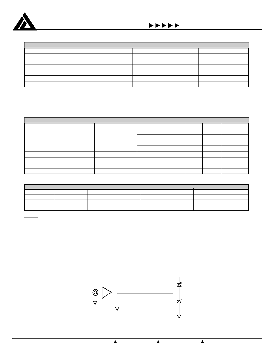
Note 1:
The test circuit depicts the Schottky diodes in their typical application. The impact of a reverse recovery time is measured
using a narrow pulse with 670- pS rise and fall times. This pulse propagates down a 60 cm, 54 ohm strip line fabricated on
a multi-layer, controlled impedance printed circuit board. In testing the ground clamp diode, the negative going edge of the
pulse causes a reflection which forces the diode under test to become forward biased. The positive going edge of the pulse
attempts to pull this diode out of forward conduction. A reverse recovery phenomenon would cause a delay between the
known arrival time of the positive edge and the observed edge due to the time it takes for the forward biased diode to actually
become reversed biased. In this measurement, however, there is no observable difference and therefore no delay for the
positive edge due to the presence of the diode. The waveforms are adjusted to individually test the ground and V
DD
clamps.
See test circuit.
Test Circuit. Line length, pulse width and duty cycle are selected such as that only one reflection is involved
in the measurement.
V
Diode
under
test
DD
Z , L
0
ABT16244A
Pulse
Generator
DIODE CHARACTERISTICS (T
A
= 0
O
to 70
O
C)