 | –≠–ª–µ–∫—Ç—Ä–æ–Ω–Ω—ã–π –∫–æ–º–ø–æ–Ω–µ–Ω—Ç: PACVGA203 | –°–∫–∞—á–∞—Ç—å:  PDF PDF  ZIP ZIP |

©
2004 California Micro Devices Corp. All rights reserved.
12/07/04
430 N. McCarthy Blvd., Milpitas, CA 95035-5112
Tel: 408.263.3214
Fax: 408.263.7846
www.calmicro.com
1
PACVGA203
VGA Port Companion Circuit
Features
∑
Single-chip solution for the VGA port interface
∑
Includes ESD protection, level shifting, and RGB
termination
∑
Seven channels of ESD protection for all VGA port
connector pins, meeting IEC-61000-4-2 Level-4
ESD requirements (8kV contact discharge)
∑
Very low loading capacitance from ESD protection
diodes on VIDEO lines; 4pF typical
∑
75
termination resistors for VIDEO lines
(matched to 1% typ.)
∑
TTL to CMOS level-translating buffers with power-
down mode for HSYNC and VSYNC lines
∑
Bi-directional level shifting N-channel FETs pro-
vided for DDC_CLK & DDC_DATA channels
∑
Compact 24-pin QSOP package
∑
Lead-free version available
Applications
∑
Notebook computers with VGA port
∑
Desktop PCs with VGA port
Product Description
The PACVGA203 incorporates seven channels of ESD
protection for all signal lines commonly found in a VGA
port. ESD protection is implemented with current
steering diodes designed to safely handle the high
surge currents encountered with IEC-61000-4-2 Level-
4 ESD Protection (8kV contact discharge). When a
channel is subjected to an electrostatic discharge, the
ESD current pulse is diverted via the protection diodes
into either the positive supply rail or ground where it
may be safely dissipated. Separate positive supply
rails are provided for the VIDEO, DDC and SYNC
channels to facilitate interfacing with low voltage Video
Controller ICs and provide design flexibility in multi-
supply-voltage environments.
Two non-inverting drivers provide buffering for the
HSYNC and VSYNC signals from the Video Controller
IC (SYNC_IN1, SYNC_IN2). These buffers accept TTL
input levels and convert them to CMOS output levels
that swing between Ground and V
CC
4 (cont'd next
page).
Simplified Electrical Schematic
VIDEO_1
VIDEO_2
VIDEO_3
3
4
5
2
6
V
CC
1
GNDD
GNDD
75
75
75
GNDA
8
9
10
TERM_1
TERM_2
TERM_3
GNDA
7
R
C
V
CC
2
DDC_IN2
17
GNDD
GNDD
GNDD
V
CC
3
18
DDC_OUT2
R
C
V
CC
2
DDC_IN1
16
GNDD
GNDD
GNDD
V
CC
3
15
DDC_OUT1
12
14
GNDD
R
B
19
GNDD
SYNC_IN1
GNDD
V
CC
4
23
SD1
V_BIAS
SYNC_OUT1
PWR_UP
1
13
20
11
R
C
GNDD
21
GNDD
SYNC_IN2
V
CC
4
1
24
SD2
GNDD
SYNC_OUT2
22
R
S
R
S
D1
©
2004 California Micro Devices Corp. All rights reserved.
2
430 N. McCarthy Blvd., Milpitas, CA 95035-5112
Tel: 408.263.3214
Fax: 408.263.7846
www.calmicro.com
12/07/04
PACVGA203
Product Description (cont'd)
These drivers have nominal 15
output impedance
(R
S
) which can be combined with an external resistor
to match the characteristic impedance of the HSYNC &
VSYNC lines of the video cables typically used in PC
applications. Two N-channel FETs provide the level
shifting function required when the DDC controller is
operated at a lower supply voltage than the monitor.
Three 75
resistors suitable for terminating the video
signals from the video DAC are also provided. These
resistors have separate input pins to allow insertion of
additional EMI filtering, if required, between the termi-
nation point and the ESD protection diodes. These
resistors are matched to better than 2% for excellent
signal level matching of the R/G/B signals.
When the PWR_UP input is driven LOW, the SYNC
inputs can be floated without causing the SYNC buffers
to draw any current from the V
CC
4 supply. When the
PWR_UP input is LOW the SYNC outputs are driven
LOW.
V
CC
3 can be derived from V
CC
4, if desired, by connect-
ing V
CC
3 to V_BIAS. In applications where V
CC
4 may
be powered down, diode D1 blocks any DC current
paths from the DDC_OUT pins back to the powered
down V
CC
4 rail via the top ESD protection diodes.
The PACVGA203 device is housed in a 24-pin QSOP
package and is available with optional lead-free finish-
ing.
Ordering Information
Note 1: Parts are shipped in Tape & Reel form unless otherwise specified.
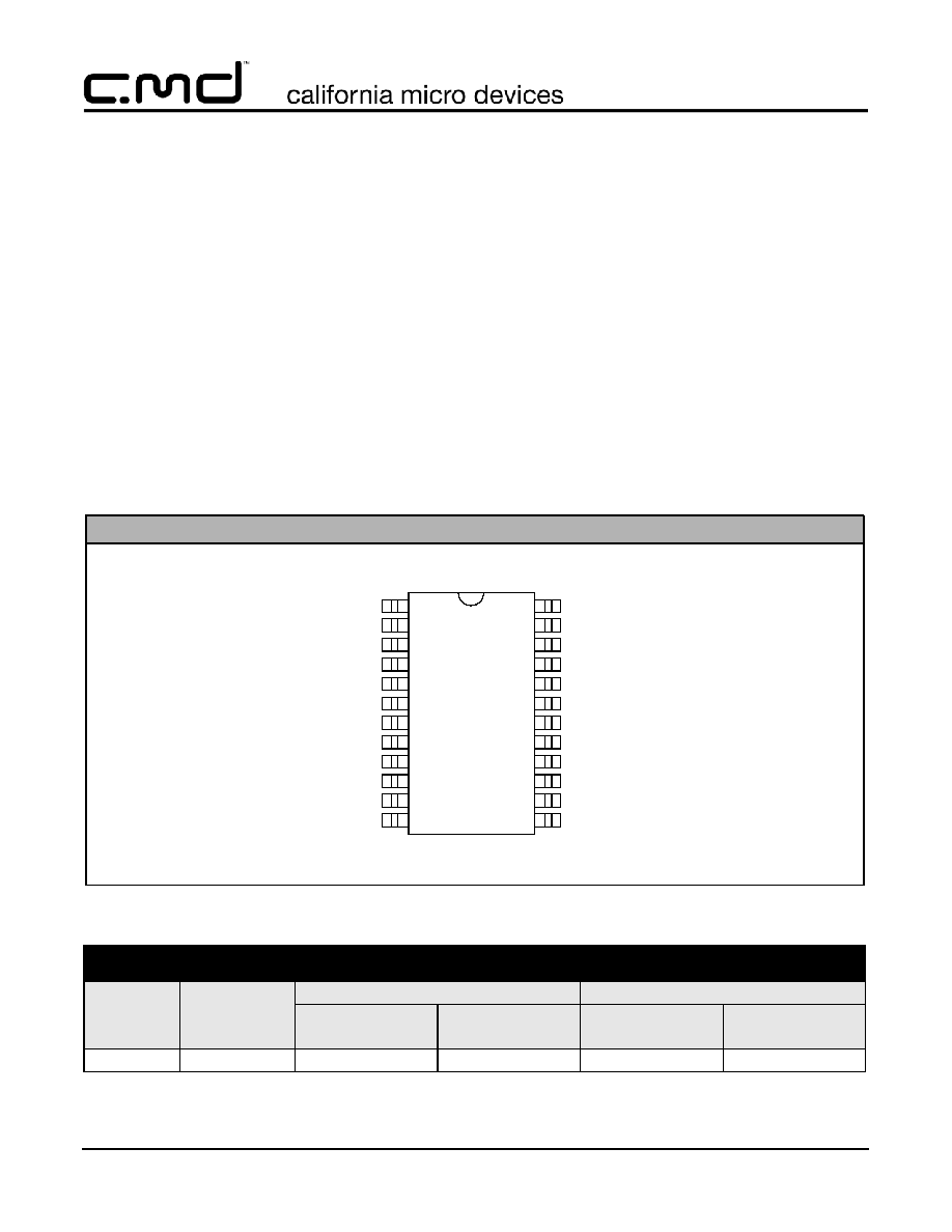
PACKAGE / PINOUT DIAGRAM
Note: This drawing is not to scale.
Top View
24-pin QSOP
1
2
3
4
5
6
7
8
16
15
14
13
17
18
9
10
20
19
21
22
11
12
23
24
VIDEO_3
GNDD
GNDA
TERM_1
TERM_2
TERM_3
PWR_UP
V
CC
2
V
CC
4
V
CC
1
VIDEO_1
VIDEO_2
SD1
SYNC_OUT2
SYNC_IN2
SYNC_OUT1
SYNC_IN1
DDC_OUT2
DDC_IN2
DDC_IN1
DDC_OUT1
V
CC
3
V_BIAS
SD2
PART NUMBERING INFORMATION
Pins
Package
Standard Finish
Lead-free Finish
Ordering Part
Number
1
Part Marking
Ordering Part
Number
1
Part Marking
24
QSOP-24
PACVGA203Q
PACVGA203Q
PACVGA203QR PACVGA203QR
©
2004 California Micro Devices Corp. All rights reserved.
12/07/04
430 N. McCarthy Blvd., Milpitas, CA 95035-5112
Tel: 408.263.3214
Fax: 408.263.7846
www.calmicro.com
3
PACVGA203
PIN DESCRIPTIONS
LEAD(s)
NAME
DESCRIPTION
1
V
CC
4
Positive voltage supply pin. This is an isolated V
CC
pin for the SYNC_1, SYNC_2, SD1
and SD2 circuits.
2
V
CC
1
Positive voltage supply pin. This is an isolated V
CC
pin for the VIDEO_1, VIDEO_2 and
VIDEO_3 ESD circuits.
3-5
VIDEO_1, VIDEO_2,
VIDEO_3
RGB Video Protection Channels. These pins tie to the RGB video lines (for example, the
Blue signal) between the VGA controller device and the video connector.
6
GNDD
Digital Ground reference supply pin.
7
GNDA
Ground reference supply pin for TERM_1, TERM_2 and TERM_3 pins.
8-10
TERM_1, TERM_2,
TERM_3
RGB Video Termination Channels. These pins tie to the RGB video lines (for example,
the Blue signal) providing a 75
termination to GNDA for the given video channel.
11
PWR_UP
Sync Signal Output 1. Ties to the video connector side of one of the sync lines (for
example the Horizontal Sync signal).
12
V
CC
2
Positive voltage supply pin. This is an isolated V
CC
pin for the DDC_IN1 and DDC_IN2
input circuits. Defines the logic one level for the DDC_OUTn outputs.
13
V_BIAS
Used to derive V
CC3
from V
CC4
input.
14
V
CC
3
Positive voltage supply pin. This is an isolated V
CC
pin for the DDC_OUT1 and
DDC_OUT2 ESD protection circuits.
15
DDC_OUT1
DDC Signal Output 1. Connects to the connector side of one of the DDC signals (for
example, the bidirectional DDC_Data serial line).
16
DDC_IN1
DDC Signal Input 1. Connects to the VGA Controller side of one of the DDC signals (for
example, the bidirectional DDC_Data serial line).
17
DDC_IN2
DDC Signal Input 2. Connects to the VGA Controller side of one of the DDC signals (for
example, the bidirectional DDC_Clk).
18
DDC_OUT2
DDC Signal Output 2. Connects to the connector side of one of the DDC signals (for
example, the bidirectional DDC_Clk).
19
SYNC_IN1
Sync Signal Buffer Input 1. Connects to the VGA Controller side of one of the sync lines
(for example, the Horizontal Sync signal).
20
SYNC_OUT1
Sync Signal Buffer Output 1. Connects to the video connector side of one of the sync
lines (for example the Horizontal Sync signal).
21
SYNC_IN2
Sync Signal Buffer Input 2. Connects to the VGA Controller side of one of the sync lines
(for example, the Vertical Sync signal).
22
SYNC_OUT2
Sync Signal Buffer Output 2. Connects to the video connector side of one of the sync
lines (for example the Vertical Sync signal).
23
SD1
Sync Signal Filter 1. Connects to the video connector side of one of the sync lines (for
example the Vertical Sync signal).
24
SD2
Sync Signal Filter 2. Connects to the video connector side of one of the sync lines (for
example the Horizontal Sync signal).

©
2004 California Micro Devices Corp. All rights reserved.
4
430 N. McCarthy Blvd., Milpitas, CA 95035-5112
Tel: 408.263.3214
Fax: 408.263.7846
www.calmicro.com
12/07/04
PACVGA203
Specifications
ABSOLUTE MAXIMUM RATINGS
PARAMETER
RATING
UNITS
V
CC
1,V
CC
2,V
CC
3, and V
CC
4 Supply Voltage
[GND - 0.5] to +6.0
V
Diode D1 Forward DC Current
100
µA
Operating Temperature Range
-40 to +85
∞C
Storage Temperature Range
-65 to +150
∞C
DC Voltage at Inputs
VIDEO_1, VIDEO_2, VIDEO_3
TERM_1, TERM_2, TERM_3
DDC_IN1, DDC_IN2
DDC_OUT1, DDC_OUT2
SYNC_IN1, SYNC_IN2
(GND - 0.5) to (V
CC
1 + 0.5)
-6.0, +6.0
(GND - 0.5) to (V
CC
2 + 0.5)
(GND - 0.5) to (V
CC
3 + 0.5)
(GND - 0.5) to (V
CC
4 + 0.5)
V
V
V
V
V
Package Power Rating
1000
mW
STANDARD OPERATING CONDITIONS
PARAMETER
RATING
UNITS
Operating Temperature Range
0 to +70
∞C
ELECTRICAL OPERATING CHARACTERISTICS
(SEE NOTE 1)
SYMBOL PARAMETER
CONDITIONS
MIN
TYP
MAX
UNITS
I
CC1
V
CC
1 Supply Current
V
CC
1 = 5.0V, VIDEO inputs at V
CC
1 or GND
level
10
µA
I
CC2
,
I
CC3
V
CC
2 & V
CC
3 Supply
Current
V
CC
2 = V
CC
3 = 5.0V
10
µA
I
CC4
V
CC
4 Supply Current
V
CC
4 = 5.0V; SYNC inputs at GND or V
CC
4
level; PWR-UP pin at V
CC
4; SYNC outputs
unloaded
10
µA
V
CC
4 = 5.0V; SYNC inputs at 3.0V; PWR-UP
pin at V
CC
4; SYNC outputs unloaded
200
µA
V
CC
4 = 5.0V; PWR-UP input at GND; SYNC
outputs unloaded
10
µA
V
BIAS
V
BIAS
Open Circuit Voltage No external current drawn from V
BIAS
pin
V
CC
4-0.8
V
R
T
Video Termination
Resistance
71.25
75
78.75
R
T
Resistance Matching
1
2
%
©
2004 California Micro Devices Corp. All rights reserved.
12/07/04
430 N. McCarthy Blvd., Milpitas, CA 95035-5112
Tel: 408.263.3214
Fax: 408.263.7846
www.calmicro.com
5
PACVGA203
Note 1: All parameters specified over standard operating conditions unless otherwise noted.
Note 2: This parameter applies only to the HSYNC and VSYNC channels. HSYNC and VSYNC have 24mA drivers with R
S
added in
series to terminate transmission line.
Note 3: Per the IEC-61000-4-2 International ESD Standard, Level 4 contact discharge method. V
CC
1, V
CC
3 and V
CC
4 must be
bypassed to GND via a low impedance ground plane with a 0.2uF, low inductance, chip ceramic capacitor at each supply
pin. ESD pulse is applied between the applicable pins and GND. ESD pulse can be positive or negative with respect to
GND. Applicable pins are: VIDEO_1, VIDEO_2, VIDEO_3, SD1, SD2, DDC_OUT1 and DDC_OUT2. All other pins are ESD
protected to the industry standard 2kV per the Human Body Model (MIL-STD-883, Method 3015).
Note 4: This parameter is guaranteed by design and characterization.
V
IH
Logic High Input Voltage
V
CC
4 = 5.0V; See Note 2
2.0
V
V
IL
Logic Low Input Voltage
V
CC
4 = 5.0V; See Note 2
0.8
V
V
OH
Logic High Output Voltage
I
OH
= -4mA, V
CC
4 = 5.0V; See Note 2
4.94
V
V
OL
Logic Low Output Voltage
I
OL
= 4mA, V
CC
4 = 5.0V; See Note 2
0.06
V
R
OH
Output Resistance
See Note 2
15
R
OL
15
R
B
,R
P
Resistor Value
PWR_UP = V
CC
3 = 5.0V
0.5
1.0
2.0
M
R
C
V
CC
2 Pull-down Resistor
Value
V
CC
2 = 3.0V
0.5
1.5
3.0
M
I
N
Input Current
VIDEO inputs
HSYNC, VSYNC inputs
V
CC
1= 5.0V; V
IN
= V
CC
1 or GND
V
CC
4 = 5.0V; V
IN
= V
CC
4 or GND
+1
+1
µA
µA
I
OFF
Off-state Leakage Current,
Level-shifting NFET
(V
CC
2 - V
DDC_IN
) < 0.4V; V
DDC_OUT
= V
CC
2
(V
CC
2 - V
DDC_OUT
) < 0.4V; V
DDC_IN
= V
CC
2
10
10
µA
µA
V
ON
Voltage drop across level
shifting NFET when turned
ON
V
CC
2= 2.5V; V
S
= GND; I
DS
= 3mA
0.15
V
C
IN
Input Capacitance
VIDEO_1,VIDEO_2 &
VIDEO_3 inputs
Note 4 applies for all cases;
V
CC
1 = 5.0V; V
IN
= 2.5V; measured at 1MHz
V
CC
1 = 2.5V; V
IN
= 1.25V; measured at 1MHz
3.0
3.0
4.0
4.5
5.0
5.6
pF
pF
t
PLH
SYNC Drivers L => H
Propagation Delay
C
L
= 50pF; V
CC
=5.0V,Input t
R
and t
F
< 5ns
8.0
12.0
ns
t
PHL
SYNC Drivers H => L
Propagation Delay
C
L
= 50pF; V
CC
=5.0V; Input t
R
and t
F
< 5ns
8.0
12.0
ns
t
R,
t
F
SYNC Drivers Output Rise
& Fall Times
C
L
= 50pF; V
CC
=5.0V; Input t
R
and t
F
< 5ns
(measured 10% - 90%)
5.0
7.0
10.0
ns
V
ESD
ESD Withstand Voltage
V
CC
1 = V
CC
3 = V
CC
4 = 5V; Notes 3 & 4
±8
kV
ELECTRICAL OPERATING CHARACTERISTICS
(SEE NOTE 1)
(CONT'D)
SYMBOL PARAMETER
CONDITIONS
MIN
TYP
MAX
UNITS

©
2004 California Micro Devices Corp. All rights reserved.
6
430 N. McCarthy Blvd., Milpitas, CA 95035-5112
Tel: 408.263.3214
Fax: 408.263.7846
www.calmicro.com
12/07/04
PACVGA203
Test Circuit Information
Average Current through V
CC
4 (I
CC
4)
The circuit in
Figure 1
was used to characterize I
CC
4 current as SYNC_IN signal frequency varies. A square wave
signal was connected to the input of one of the SYNC buffers (i.e. pin 19 or pin 21). The frequency of this signal
was varied between 0 and 100 kHz. The risetime and falltime was kept constant at 10ns. Three different values of
C1 were used: 0pF, 50pF and 100pF. The results are plotted in
Figure 2
.
Figure 1. Sync Buffer I
CC
4 Test Circuit
Figure 2. I
CC
4 vs. SYNC_IN Frequency Performance Data
0V
V
CC
4
+5V
SYNC_IN
I
CC
4
C1
SYNC_OUT
3.3V
I
CC4
vs. SYNC_IN Frequency
0
10
20
30
40
50
60
70
80
90
100
0
20
40
60
80
100
Frequency, kHz
I
CC4
,u
A
100pF
50pF
0pF
©
2004 California Micro Devices Corp. All rights reserved.
12/07/04
430 N. McCarthy Blvd., Milpitas, CA 95035-5112
Tel: 408.263.3214
Fax: 408.263.7846
www.calmicro.com
7
PACVGA203
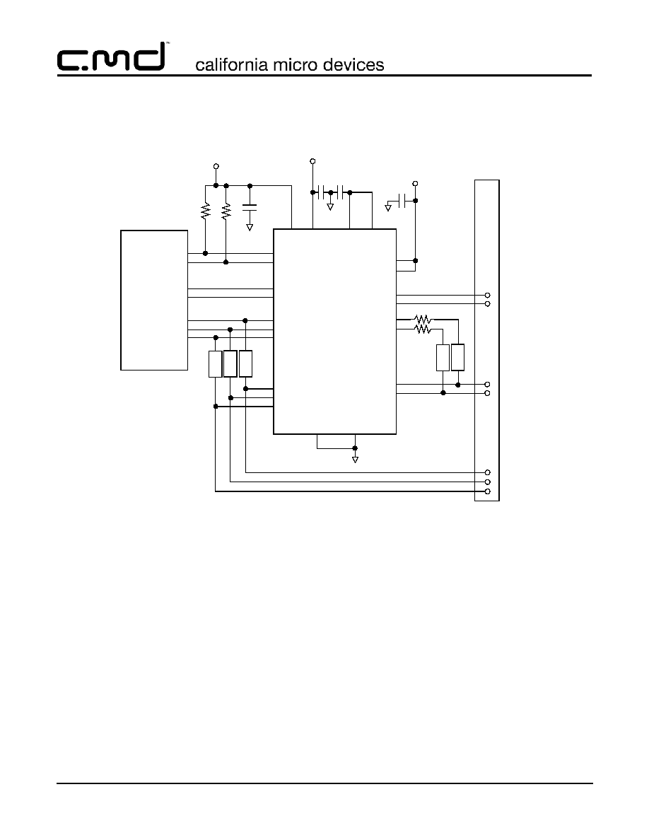
Application Information
Figure 3. Typical Connection Diagram
A resistor may be necessary between the V
CC
3 pin and ground if protection against a stream of ESD pulses is
required while the PACVGA203 is in the power-down state. The value of this resistor should be chosen such that
the extra charge deposited into the V
CC
3 bypass capacitor by each ESD pulse will be discharged before the next
ESD pulse occurs. The maximum ESD repetition rate specified by the IEC-61000-4-2 standard is one pulse per
second. When the PACVGA203 is in the power-up state, an internal discharge resistor is connected to ground via
an FET switch for this purpose.
For the same reason, V
CC
1 and V
CC
4 may also require bypass capacitor discharging resistors to ground if there
are no other components in the system to provide a discharge path to ground.
GNDA, the reference voltage for the 75
resistors is not connected internally to GNDD and should ideally be con-
nected to the ground of the video DAC IC.
Red
R1
R2
8
9
10
19
21
16
17
7
6
14
2
12
Video
Co
nne
cto
r
V
i
de
o Co
nt
ro
ller
H-Sync
V-Sync
DDC_Data
DDC_Clk
Blue
Grn
H-Sync
V-Sync
DDC_Data
DDC_Clk
R
G
B
PACVGA203
GNDA
GNDD
DDC_IN1
DDC_IN2
SYNC_IN1
SYNC_IN2
TERM_1
TERM_2
TERM_3
3
VIDEO_1
VIDEO_2
VIDEO_3
4
5
VF*
*
VF*
*
VF**
0.2uF
V
CC
2 V
CC
1
V
CC
4
PWR_UP
DDC_OUT1
DDC_OUT2
SYNC_OUT1
SYNC_OUT2
18
15
22
20
VIDEO_DAC_V
CC
13
V
CC
3 V_BIAS
0.2uF
GNDD
0.2uF
0.2uF
GNDD
SD1
SD2
24
SF*
*
SF**
23
11
1
DDC_V
CC
5V
VF** - VIDEO EMI Filter
SF** - SYNC EMI Filter
SR*
SR*
SR* - external resistor to
match video cable
characteristic
impedance.

©
2004 California Micro Devices Corp. All rights reserved.
8
430 N. McCarthy Blvd., Milpitas, CA 95035-5112
Tel: 408.263.3214
Fax: 408.263.7846
www.calmicro.com
12/07/04
PACVGA203
Mechanical Details
QSOP Mechanical Specifications:
PACVGA203 devices are packaged in 24-pin QSOP
packages. Dimensions are presented below.
For complete information on the QSOP-24 package,
see the California Micro Devices QSOP Package Infor-
mation document.
* This is an approximate number which may vary.
Package Dimensions for QSOP-24
PACKAGE DIMENSIONS
Package
QSOP (JEDEC name is SSOP)
Pins
24
Dimensions
Millimeters
Inches
Min
Max
Min
Max
A
1.35
1.75
0.053
0.069
A1
0.10
0.25
0.004
0.010
B
0.20
0.30
0.008
0.012
C
0.18
0.25
0.007
0.010
D
8.56
8.73
0.337
0.344
E
3.81
3.98
0.150
0.157
e
0.64 BSC
0.025 BSC
H
5.79
6.19
0.228
0.244
L
0.40
1.27
0.016
0.050
# per tube
55 pcs*
# per tape
and reel
2500 pcs
Controlling dimension: inches
Mechanical Package Diagrams
E
D
H
TOP VIEW
L
END VIEW
C
e
B
A
A1
SEATING
PLANE
SIDE VIEW
5
6
7
8
9
10
1
2
3
4
20 19 18 17 16 15
24 23 22 21
Pin 1 Marking
11 12
14 13