 | –≠–ª–µ–∫—Ç—Ä–æ–Ω–Ω—ã–π –∫–æ–º–ø–æ–Ω–µ–Ω—Ç: CLM2931-3 | –°–∫–∞—á–∞—Ç—å:  PDF PDF  ZIP ZIP |
Low Dropout
Voltage Regulators
CLM2931
FEATURES
∑
∑
5V, 3.3V, 3.5V, 4.0V, and 4.5V Versions Available
∑
∑
Output Current in Excess of 100mA
∑
∑
Input-Output Differential is Less Than 0.6V
∑
∑
Mirror-Image Insertion Protection
∑
∑
Internal Thermal Overload Protection
∑
∑
Available as Adjustable with TTL Compatible Switch
∑
∑
Similar to Industry Standard LM2931
∑
∑
Reverse Battery Protection
∑
∑
Short Circuit Protection
∑
∑
60V Load Dump Protection
∑
∑
-50V Reverse Transient Protection
APPLICATIONS
∑
∑
Portable Instrumentation
∑
∑
Radio Control Systems
∑
∑
Cordless Telephones
PRODUCT DESCRIPTION
The CLM2931 is a positive low power voltage regulator. This
device is an excellent choice for use in battery-powered
applications such as cordless telephones, radio control
systems, and portable computers. The CLM2931 features very
low quiescent current (0.4mA) and very low drop output voltage
(typ. 50mV at light load and 300mV at 100mA). other features
include the logic-compatible on/off input which enables the
regulator to be switched on and off.
The regulator output voltage may be internally pin-strapped
for a 5V, 3V, 3.3V, 3.5V, 4.0V, 4.5V or programmed from 3V to
24V with an external pair of resistors. Using Calogic's design,
process and testing technique make the CLM2931 superior
over similar products.
ORDERING INFORMATION
PART
PACKAGE
TEMPERATURE RANGE
CLM2931AS-X
Plastic SOIC (8-Pin)
Industrial
X = Output Voltage, 5V = standard product, for all other ranges
contact factory.
CORPORATION
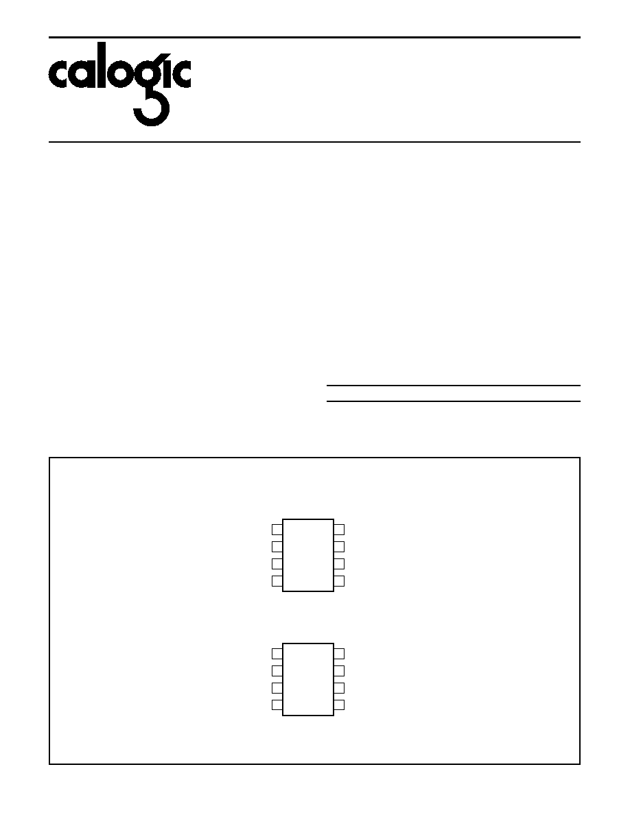
PIN CONNECTIONS
ADJ.
1
2
3
8
7
6
4
5
ON/OFF
CLM2931
1M-07
8-PIN SRFACE MOUNT, ADJ. OUTPUT
GND
GND
INPUT
GND
GND
OUTPUT
TOP VIEW
NC
1
2
3
8
7
6
4
5
NC
CLM2931
8-PIN SURFACE MOUNT, FIX OUTPUT
GND
GND
INPUT
GND
GND
OUTPUT
TOP VIEW
CALOGIC CORPORATION, 237 Whitney Place, Fremont, California 94539, Telephone: 510-656-2900, FAX: 510-651-3025

ABSOLUTE MAXIMUM RATINGS
Power Dissipation . . . . . . . . . . . . . . . . . . . . . Internally Limited
Lead Temp. (Soldering, 5 Seconds) . . . . . . . . . . . . . . . 260
o
C
Storage Temperature Range . . . . . . . . . . . . . . . -65 to +150
o
C
Operating Junction Temperature Range . . . . . . . -40 to +85
o
C
Input Supply Voltage . . . . . . . . . . . . . . . . . . . . . . 0.30 to +26V
ESD Rating . . . . . . . . . . . . . . . . . . . . . . . . . . . . . . . . . . . . 2KV
CLM2931
CORPORATION
CALOGIC CORPORATION, 237 Whitney Place, Fremont, California 94539, Telephone: 510-656-2900, FAX: 510-651-3025
ELECTRICAL CHARACTERISTICS: V
S
= 14V, T
A
= 25
o
C, I
O
= 10mA, C2 = 100
µ
F, unless otherwise specified. (Note 1)
PARAMETER
CLM2931A
CLM2931
UNITS
CONDITIONS
(Note 2)
MIN
TYP
MAX
MIN
TYP
MAX
3V VERSION
CLM2931A-3
CLM2931-3
Output Voltage
2.94
2.88
3.0
3.0
3.06
3.12
2.91
2.85
3.0
3.0
3.09
3.15
V
V
6V<V
IN
<26V, I
O
= 100mA Over Temp.
3.3V VERSION
CLM2931A-3.3
CLM2931-3.3
Output Voltage
3.23
3.20
3.30
3.30
3.36
3.39
3.20
3.16
3.30
3.30
3.39
3.43
V
V
6V<V
IN
<26V, I
O
= 100mA Over Temp.
5V VERSION
CLM2931A-5
CLM2931-5
Output Voltage
4.81
4.75
5.0
5.19
5.25
4.75
4.50
5.0
5.25
5.50
V
V
6V<V
IN
<26V, I
O
= 100mA Over Temp.
ALL VOLTAGE OPTIONS
Long Term Stability
20
20
mV/1000
Line Regulation
2.0
4.0
10
30
4.0
30
mV
9V<V
IN
<16V
6V<V
IN
<26V
Load Regulation
14
50
14
50
mV
5mA<I
O
<100mA
Dropout Voltage
0.05
0.07
0.3
0.2
0.1
0.6
0.05
0.07
0.3
0.2
0.1
0.6
V
V
V
I
O
= 10mA
I
O
= 50mA
I
O
= 100mA
Quiescent Current
0.4
15
1.0
0.4
15
1.0
mA
mA
I
O
<10mA,6V<V
IN
<26V, -40
o
C<T
J
<125
o
C
I
O
= 100mA, V
IN
= 14V, T
J
= 25
o
C
Maximum Operational
Input Current
26
33
26
33
V
Maximum Line Transient
60
70
70
50
V
R
L
= 500
, V
O
<5.5V, 100ms
Reverse Polarity Input
Voltage, DC
-15
-30
-15
30
V
V
O
>-0.3V, R
L
= 500
Reverse Polarity Input
Voltage, Transient
-50
-80
-50
-80
V
1% Duty Cycle,
<100ms, R
L
= 500
Output Noise Voltage
500
500
µ
Vrms
10Hz-100kHz, C
OUT
= 100
µ
F
Ripple Rejection
80
80
dB
f
O
= 120Hz

CLM2931
CORPORATION
CALOGIC CORPORATION, 237 Whitney Place, Fremont, California 94539, Telephone: 510-656-2900, FAX: 510-651-3025
ADJUSTABLE VERSION ONLY: V
IN
= 14V, V
O
= 3V, I
O
= 10mA, R1 = 27k, C2 = 100
µ
F, T
J
= 25
o
PARAMETER
CLM2931C
UNITS
CONDITIONS
MIN
TYP
MAX
Output Voltage Range
3.0
24
V
Line Regulation
0.2
1.5
mV
V
OUT
+ 0.6V<V
IN
<26V
Load Regulation
0.3
1.0
mV
5mA<I
O
<100mA
Output Impedance
40
m
/V
100mADC and 10mArms, 100Hz-10kHz
Quiescent Current
0.4
15
0.8
1.0
1.0
mA
mA
mA
I
O
= 10mA
I
O
= 100mA
During Shutdown R
L
= 500
Output Noise Voltage
100
µ
Vrms
10Hz-100kHz
Long Term Stability
0.4
%/1000h
Ripple Rejection
0.02
%/V
f
O
= 120Hz
Dropout Voltage
0.05
0.3
0.2
0.6
V
V
I
O
< 10mA
I
O
= 100mA
Maximum Operational Input Voltage
26
33
V
Maximum Line Transient
60
70
V
I
O
= 10mA, Reference Voltage <1.5V
Reverse Polarity Input Voltage, DC
-15
-30
V
V
O
>-0.3V, R
L
= 500
Reverse Polarity Input Voltage, Transient
-50
-80
V
1% Duty Cycle, T<100ms, R
L
= 500
On/Off Threshold Current
20
50
µ
A
Threshold Votage
On
Off
3.25
2.0
2.2
1.2
V
V
O
= 3V
Note 1: See TYPICAL APPLICATIONS notes to ensure constant junction temperature, low duty cycle pulse testing used.
Note 2: All limits are at 25
o
C or over the full operating temperature junction range of -40
o
C to +125
o
C.
Note 3: The maximum power dissipation is a function of maximum junction temperature, total thermal resistance, and ambient temperature.
Note 4: Human body model, 100
µ
F discharged through 1.5K
.
APPLICATION HINTS
The CLM2931 requires an output capacitor for device stability.
The value required varies greatly depending upon the
application circuit and other factors. The high frequency
characteristics of electolytic capacitors depend greatly on the
type and also on the manufacturer. Sometimes only bench
testing is the only means to determine the proper capacitor
type and value. The high quality 100
µ
F aluminum electrolytic
covers all general application circuits, this stability can be
obtained with a tantalum electrolytic value of 47
µ
F.
Another critical point of electrolytic characteristics is its
performance over temperature. The CLM2931 is designed to
operate starting at -40
o
C which may not be true in the case of
electrolytic. Higher temperatures are generally no problem.
The electrolytic type in aluminum will freeze at around -30
o
C.
This could cause an oscillation at output of regulator. At a
lower temperature requirement by many applications the
capacitor should maintain its performance. So as a result, for an
application which regulator junction temperature does not exceed
25
o
C, the output capacitor can be reduced by the factor of two
over the value needed for the entire temperature range.
Other points with linear regulators is that the twitch higher
output current stability decreases. In most applications the
CLM2931 is operating at a few milliamps. In these
applications the output capacitance can be further reduced.
For example, when the regulator is running at 10mA output
current the output capacitance value is half compared to the
same regulator that is running at 100mA.
With the CLM2931CT adjustable regulator, the minimum value
of output capacitance is a function of the output voltage. The
value decreases with higher output voltages, since the
internal loop gain is reduced.
The worst case occurs at the lower temperature and
maximum operating currents, the entire circuit and the
electrolytic, should be cooled down to the minimum
temperature. The minimum of 0.6 volts required at the input
of regulator above the output to keep the power dissipation
and die heating to its minimum. After the value for the
capacitor has been determined for actual use, the value
should be doubled.
CALOGIC CORPORATION, 237 Whitney Place, Fremont, California 94539, Telephone: 510-656-2900, FAX: 510-651-3025
CLM2931
CORPORATION
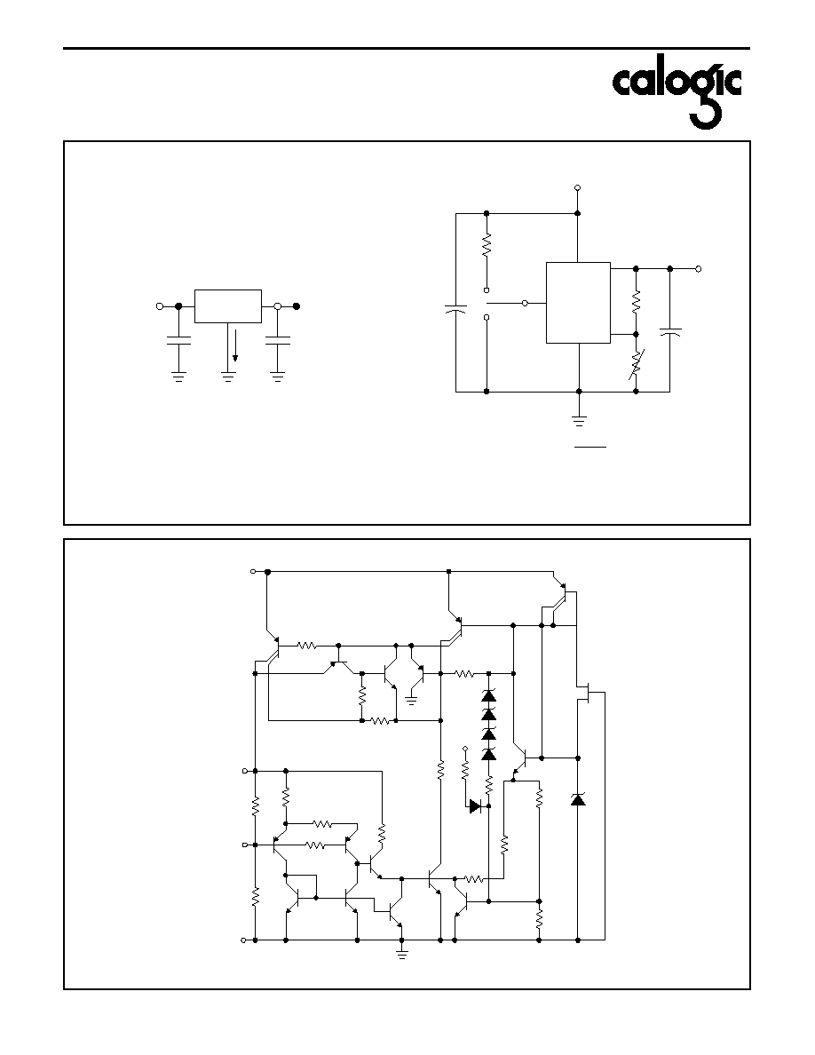
TYPICAL APPLICATIONS
CLM2931 FIXED OUTPUT
UNREGULATED
INPUT
V
REGULATED
OUTPUT
C1
0.1
GND
I
Q
+
C2
100
µ
F
OUT
CLM2931
1M-06
V
IN
V
CC
IN
OUT
ON/OFF
V
OUT
R1
20k
C2
100
µ
F
R2
ADJ
GND
ON
OFF
R3
51k
C1
0.1
µ
F
CLM2931
ADJUSTABLE
V = Reference Voltage x
OUT
R1 + R2
R1
1M-09
CLM2931 FIXED OUTPUT
CLM2931 ADJUSTABLE OUTPUT
SCHEMATIC DIAGRAM
V
IN
Q1
V
OUT
R1
5V: 20k
ADJ:
ADJUST
R2
5V: 100k
ADJ:
GND
R6
6
Q2
Q10 Q3
R16
6k
R19
200
1
1
Q12
Q13
1
5
R7
30k
Z1
Z2
Z3
Z4
ON/OFF
R11
50k
R13
40k
D1
D15
140k
Q15
R8
3k
R14
184k
Z6
R16
14.7k
R12
140k
R10
30k
Q11
Q9
Q16
Q8
Q7
Q6
Q4
R5
2.1k
R4
3.6k
R3
32k
Q5
4x
1M-08

CALOGIC CORPORATION, 237 Whitney Place, Fremont, California 94539, Telephone: 510-656-2900, FAX: 510-651-3025
CLM2931
CORPORATION
TYPICAL PERFORMANCE CHARACTERISTICS
O
U
PU
T
IM
P
E
D
AN
C
E
(
)
OUTPUT IMPEDANCE
1M-22
FREQUENCY (Hz)
10
0.01
1
0.1
1
10
100
1k
10k
100k
1M
I
O
= 10mA
LM2931 - 3.0
70
60
50
40
30
20
10
0
1M-23
OPERATION DURING
LOAD DUMP
OU
T
P
U
T
VOLTAG
E
(V)
TIME (ms)
C
O
= 100
µ
F
IN
PUT
V
O
LTAGE (
V
)
6
4
2
0
-2
-100
0
100
200
300
400
500
R
L
= 500
= 150ms
OUTPUT VOLTAGE (V)
REF
E
RENC
E VO
LT
AGE (
V
)
1.30
1.28
1.26
1.24
1.22
1.20
1.18
1.16
1.14
1.12
1.10
1M-24
REFERENCE VOLTAGE
0
LM2031C ADJUSTABLE
3
6
9
12
15
18
21 24
JUNCTION TEMPERATURE (∞C)
0.6
0.5
0.4
0.3
0.2
0.1
0
1M-25
DROPOUT VOLTAGE
I
N
PU
T
-
O
U
T
P
UT
DI
F
F
E
RE
N
T
I
A
L
(V)
0
40
80
120
I
O
= 50mA
I
O
= 10mA
I
O
= 100mA
OUTPUT CURRENT (mA)
1M-26
DROPOUT VOLTAGE
I
N
P
U
T-OU
T
P
UT D
I
FFER
E
NTI
A
L (V)
0
50
0.6
0.5
0.4
0.3
0.2
0.1
0
100
INPUT VOLTAGE (V)
O
U
T
P
UT
VO
L
T
AG
E
(
V
)
6.0
5.0
4.0
3.0
2.0
1.0
1M-27
LOW VOLTAGE BEHAVIOR
2.0
3.0
4.0
5.0
6.0
I
O
= 100mA
LM2931-5.0

CALOGIC CORPORATION, 237 Whitney Place, Fremont, California 94539, Telephone: 510-656-2900, FAX: 510-651-3025
CLM2931
CORPORATION
TYPICAL PERFORMANCE CHARACTERISTICS (continued)
INPUT VOLTAGE (V)
600
500
400
300
200
100
0
1M-28
PEAK OUTPUT CURRENT
O
U
TPU
T
CU
RRENT
(
m
A)
0
10
20
30
T
J
= 25∞C
T
J
= 85∞C
T
J
= -40∞C
OUTPUT CURRENT (mA)
0
1M-29
QUIESCENT CURRENT
30
25
20
15
10
5
Q
U
IESCENT
CUR
RENT
(
m
A)
0
30
60
90
V
IN
= 14V
25
0
1M-30
QUIESCENT CURRENT
20
15
10
3
2
1
Q
U
I
E
SC
ENT
CU
RREN
T
(
m
A)
-40
0
40
80
120
JUNCTION TEMPERATURE (∞C)
I
O
= 50mA
I
O
= 0mA
AMBIENT TEMPERATURE (∞C)
POW
E
R DI
S
S
I
P
ATIO
N (
W
)
1.0
0.9
0.8
0.7
0.6
0.5
0.4
0.3
0.2
0.1
0
1M-31
MAXIMUM POWER DISSIPATION
(SO-8)
0
20
40
60
80
10
30
50
70
90
AMBIENT TEMPERATURE (∞C)
POW
E
R DI
S
S
I
P
ATIO
N (
W
)
22
20
18
16
14
12
10
8
6
4
2
0
1M-32
MAXIMUM POWER DISSIPATION
(TO-220)
0
20
40
60
80
10
30
50
70
90 100
INFINITE HEATSINK
10∞C/W HEAT SINK
NO HEAT SINK
AMBIENT TEMPERATURE (∞C)
POW
E
R DI
S
S
I
P
ATIO
N (
W
)
1.0
0.9
0.8
0.7
0.6
0.5
0.4
0.3
0.2
0.1
0
1M-33
MAXIMUM POWER DISSIPATION
(TO-92)
0
20
40
60
80
10
30
50
70
90
0.125" LEAD LENGTH
FROM PC BOARD
0.4" LEAD LENGTH
FROM PC BOARD