High-Speed Analog
N-Channel DMOS FETs
Improved On -Resistance
SD310 / SD312 / SD314
FEATURES
∑
∑
High Input to Output Isolation . . . . . . . . . . . . . . . . 120dB
∑
∑
Low On Resistance . . . . . . . . . . . . . . . . . 15 Ohms @ 15V
∑
∑
Low Feedthrough and Feedback Transients
∑
∑
Low Capacitance:
-- Input (Gate) . . . . . . . . . . . . . . . . . . . . . . . . . . 2.4pF typ.
-- Output . . . . . . . . . . . . . . . . . . . . . . . . . . . . . . 1.3pF typ.
-- Feedback . . . . . . . . . . . . . . . . . . . . . . . . . . . . 0.3pF typ.
∑
∑
No Protection Diode from Gate to Substrate for very
high impedance applications
∑
∑
Maximum Gate Voltage . . . . . . . . . . . . . . . . . . . . . . .
±
40V
APPLICATIONS
SD310:
∑
∑
Analog Switch Driver
SD312 and SD314:
∑
∑
Analog Switches
∑
∑
High-Speed Digital Switches
∑
∑
Multiplexers
∑
∑
A to D Converters
∑
∑
D to A Converters
∑
∑
Choppers
∑
∑
Sample & Hold
DESCRIPTION
The Calogic SD310 is a 30V analog switch driver without a
built-in protection diode from gate to substrate for use with
SD312 and SD314 DMOS analog switches.
The SD312 is a high performance, high-speed, high-voltage,
and low resistance analog switch capable of switching
±
5V
signals. The maximum threshold of 2V permits simple direct
TTL an CMOS driving for small applications.
The SD314 is DMOS analog switch capable of switching
±
10V analog signals with all other parameters identical to
those of SD312.
All three devices are manufactured with an implanted
high-speed, high-voltage, and low resistance double-diffused
MOS (DMOS) process. SD310, SD312 and SD314 devices
also have no built-in protection diode to enhance performance
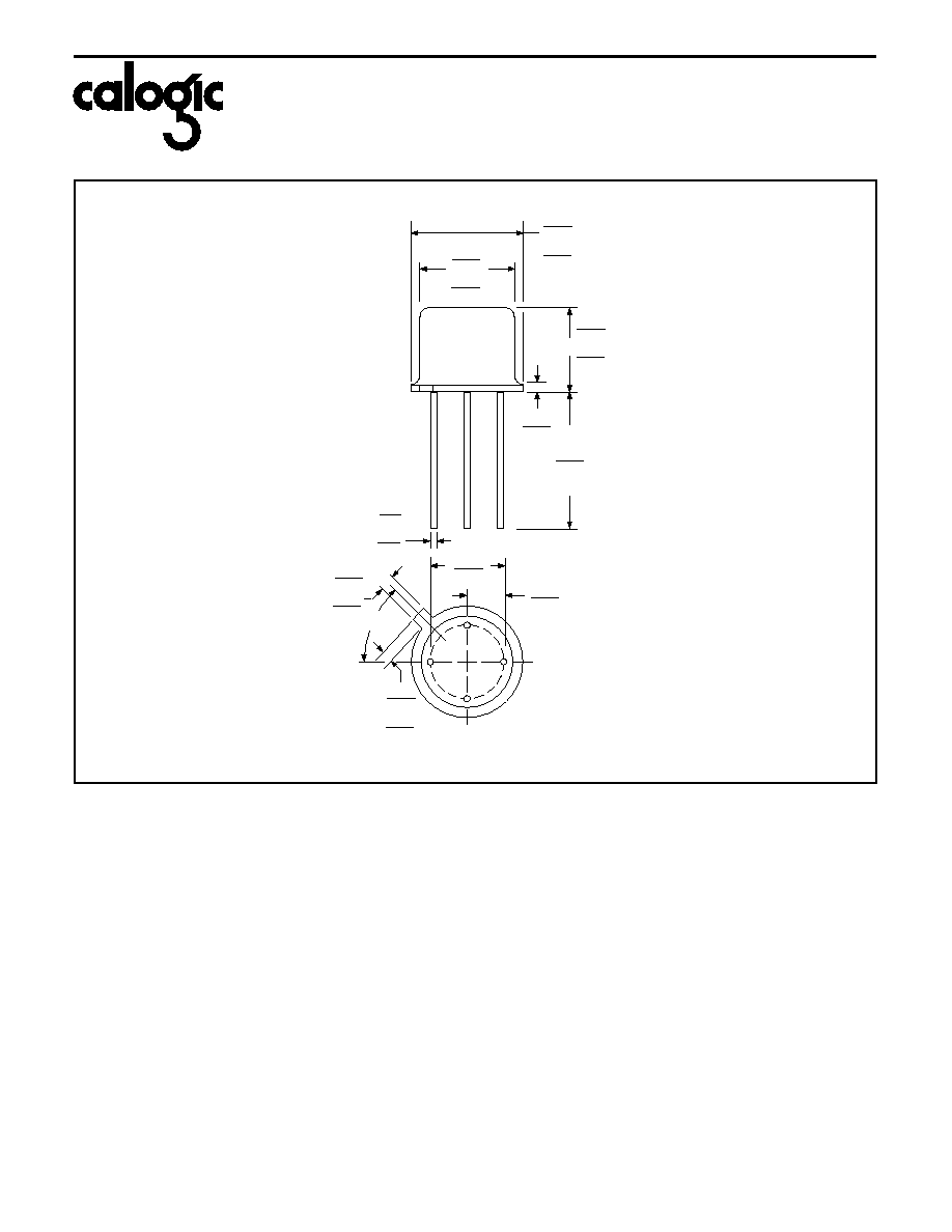
in high impedance circuits. The devices are available in
4-lead hermetic TO-72 package and in die form for hybrid
applications. Custom devices based on SD310, SD312 and
SD314 can also be ordered.
ORDERING INFORMATION
Part
Package
Temperature Range
SD310DE
Hermetic TO-72 Package
-55
o
C to +125
o
C
SD312DE
Hermetic TO-72 Package
-55
o
C to +125
o
C
SD314DE
Hermetic TO-72 Package
-55
o
C to +125
o
C
XSD310
Sorted Chips in Carriers
-55
o
C to +125
o
C
XSD312
Sorted Chips in Carriers
-55
o
C to +125
o
C
XSD314
Sorted Chips in Carriers
-55
o
C to +125
o
C
CORPORATION
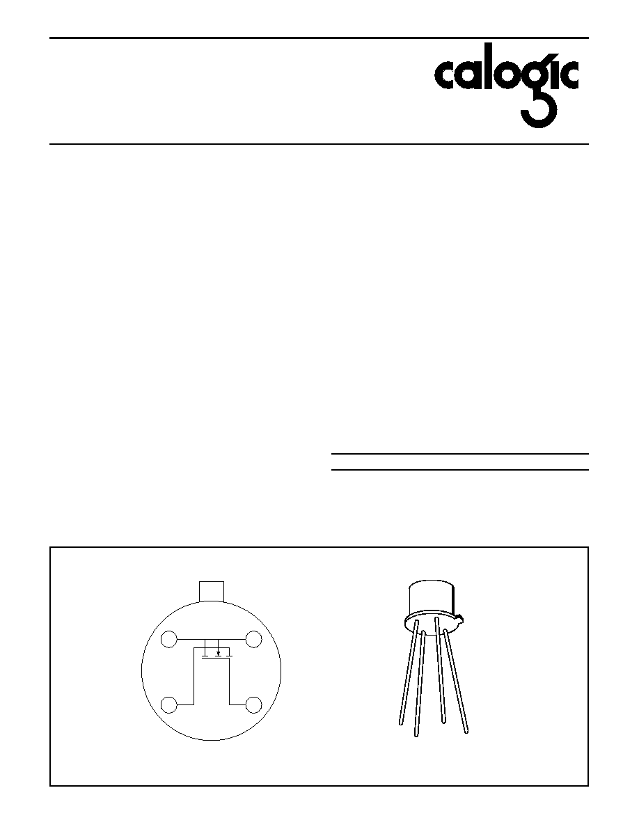
SCHEMATIC DIAGRAM (Top View)
SOURCE
BODY
AND
CASE
GATE
DRAIN
Body is internally connected to the case
1
2
3
4
CD10-2
TO-72
G
D
C
S
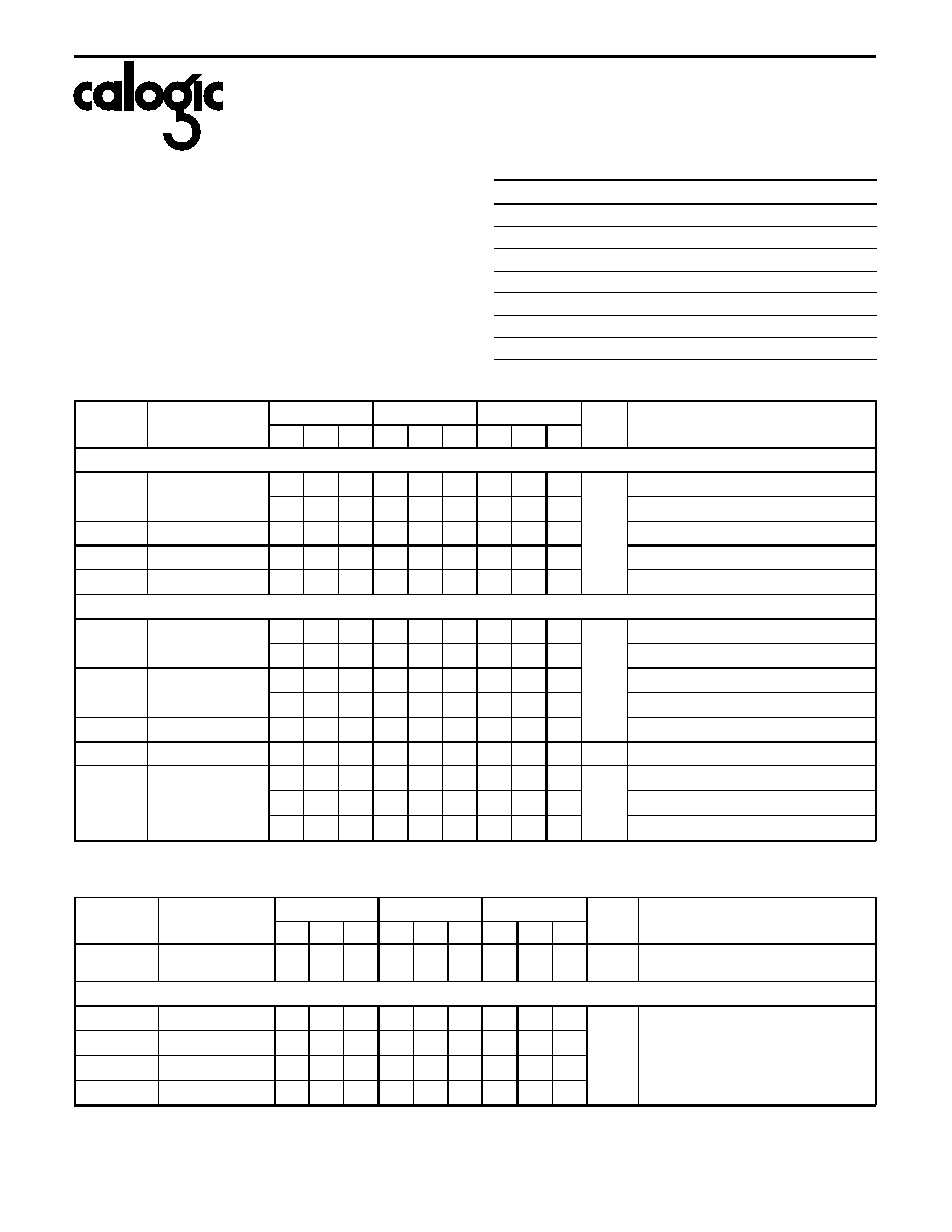
ABSOLUTE MAXIMUM RATINGS
Drain Current . . . . . . . . . . . . . . . . . . . . . . . . . . . . . . . . . . 50mA
Total Device Dissipation at 25
o
C Case Temperature . . . 1.2W
Storage Temperature Range . . . . . . . . . . . . . . -65
o
to +200
o
C
Lead Temperature (1/16" from case for 10 sec.). . . . . . 300
o
C
Operating Temperature Range . . . . . . . . . . . -55
o
C to +125
o
C
PARAMETER
SD310
SD312
SD314
UNIT
V
DS
Drain-to-source
+30
+10
+20
V
dc
V
SD
Source-to-drain*
+10
+10
+20
V
dc
V
DB
Drain-to-body
+30
+15
+25
V
dc
V
SB
Source-to-body
+15
+15
+25
V
dc
V
GS
Gate-to-source
±
40
±
40
±
40
V
dc
V
GB
Gate-to-body
±
40
±
40
±
40
V
dc
V
GD
Gate-to-drain
±
40
±
40
±
40
V
dc
SD310 / SD312 / SD314
CORPORATION
SYMBOL
PARAMETER
SD310
SD312
SD314
UNITS
TEST CONDITIONS
MIN TYP MAX MIN TYP MAX MIN TYP MAX
BREAKDOWN VOLTAGE
BV
DS
Drain-to-source
30
35
V
V
GS
= V
BS
= 0V, I
D
= 10
µ
A
10
25
10
25
20
25
V
GS
= V
BS
= -5V, I
S
= 10nA
BV
SD
Source-to drain
10
10
20
V
GD
= V
BD
= -5V, I
D
= 10nA
BV
DB
Drain-to-body
15
15
25
V
GB
= 0V, source OPEN, I
D
= 10nA
BV
SB
Source-to-body
15
15
25
V
GB
= 0V, drain OPEN, I
S
= 10
µ
A
LEAKAGE CURRENT
I
DS
(OFF)
Drain-to-source
1
10
1
10
nA
V
GS
= V
BS
= -5V, V
DS
= +10V
1
10
V
GS
= V
BS
= -5V, V
DS
= +20V
I
SD
(OFF)
Source-to-drain
1
10
1
10
V
GS
= V
BD
= -5V, V
SD
= +10V
1
10
V
GS
= V
BD
= -5V, V
SD
= +20V
I
GBS
Gate
0.1
0.1
0.1
V
DB
= V
SB
= 0V, V
GS
=
±
40V
V
T
Threshold voltage
0.5
1.0
2.0
0.5
1.0
2.0
0.5
1.0
2.0
V
V
DS
= V
GS
= V
T
, I
S
= 1
µ
A, V
SB
= 0V
r
DS
(ON)
Drain-to-source
resistance
30
50
30
50
30
50
I
D
= 1.0mA, V
SB
= 0, V
GS
= +5V
20
35
20
35
20
35
I
D
= 1.0mA, V
SB
= 0, V
GS
= +10V
15
25
15
15
I
D
= 1.0mA, V
SB
= 0, V
GS
= +15V
SYMBOL
PARAMETER
SD310
SD312
SD314
UNITS
TEST CONDITIONS
MIN TYP MAX MIN TYP MAX MIN TYP MAX
gfs
Forward
transconductance
15
20
15
20
15
20
mmhos
V
DS
= 10V, V
SB
= 0V, I
D
= 20mA,
f = 1kHz
SMALL SIGNAL CAPACITANCES (See capacitance model)
C
(GS+GD+GB)
Gate node
2.4
3.7
2.4
3.7
2.4
3.7
pF
V
DS
= 10V, f = 1MHz
V
GS
= V
BS
= -15V
C
(GD+DB)
Drain node
1.3
1.7
1.3
1.7
1.3
1.7
C
(GS+SB)
Source node
3.5
4.5
3.5
4.5
3.5
4.5
C
DG
Reverse transfer
0.3
0.7
0.3
0.7
0.3
0.7
AC ELECTRICAL CHARACTERISTICS
DC ELECTRICAL CHARACTERISTICS (T
A
= 25
o
C, unless other specified.)