
High Speed DMOS
N-Channel Switch
SD403
FEATURES
∑
∑
Ultra High Speed Switching . . . . . . . . . . . . . . . . . t
r
< 1ns
∑
∑
Very Low Capacitance. . . . . . . . . . . . . . c
rss
0.4pf typical
∑
∑
CMOS and TTL Compatible Input
∑
∑
Low ON Resistance . . . . . . . . . . . . . . . . . 40 ohms typical
APPLICATIONS
∑
∑
Switch Drivers
∑
∑
Video Switches
∑
∑
Samples and Hold
∑
∑
Track and Hold
∑
∑
VHF/UHF Amplifiers
DESCRIPTION
The Calogic SD403 is an N-Channel Enhancement-Mode
Lateral DMOS FET. This product has very low capacitance,
(c
rss
< 0.4pf typical) allowing for high speed switching (t
r
1ns).
The SD403 is a high gain device (19mmhos) and has good
performance values for sample and hold circuits, video
switches and switch drivers where lower capacitance and high
speed switching are critical.
ORDERING INFORMATION
Part
Package
Temperature Range
SD403BD Plastic TO-92
-55 to +125
o
C
SD403CY SOT-143 Surface Mount
-55 to +125
o
C
XSD403
Sorted Chips in Carriers
-55 to +125
o
C
CORPORATION
PIN CONFIGURATION
D
S G
TO-92
SCHEMATIC DIAGRAM
BODY (4)
SOURCE (1)
DRAIN (2)
GATE (3)
SOT-143
CD1-1
SOURCE
(1)
GATE
(3)
DRAIN
(2)
TO-92
GATE
(3)
DRAIN
(2)
BODY
(4)
SOURCE
(1)
SOT-143
PRODUCT MARKING
SD403CY
SD403

SD403
CORPORATION
ABSOLUTE MAXIMUM RATINGS (T
A
= +25
o
C unless otherwise noted)
Drain-Source Voltage . . . . . . . . . . . . . . . . . . . . . . . . . . . +15V
Gate-Source Voltage . . . . . . . . . . . . . . . . . . . . . . . . . . . . -0.3V
+20V
Gate-Drain Voltage . . . . . . . . . . . . . . . . . . . . . . . . . . . . . -0.3V
+20V
Source-Drain Voltage . . . . . . . . . . . . . . . . . . . . . . . . . . . -0.3V
Continuous Drain Current . . . . . . . . . . . . . . . . . . . . . . . 50mA
Power Dissipation (at or below T
A
= +25
o
C) . . . . . . . . 300mW
Linear Derating Factor . . . . . . . . . . . . . . . . . . . . . . 3.0mW/
o
C
Operating Junction and Storage
Temperature Range . . . . . . . . . . . . . . . . -55
o
C to +125
o
C
ELECTRICAL CHARACTERISTICS (T
A
= +25
o
C unless otherwise specified)
SYMBOL
CHARACTERISTICS
MIN
TYP
MAX
UNIT
TEST CONDITIONS
STATIC
BV
DSS
Drain-Source
Breakdown
Voltage
15
25
V
I
D
= 1.0
µ
A, V
GS
=0
I
D(OFF)
Drain-Source OFF Leakage Current
1.0
µ
A
V
DS
= 15V, V
GS
= 0
I
GSS
Gate-Source Leakage Current
1.0
µ
A
V
GS
= 20V, V
DS
= 0
I
D(ON)
Drain-Source ON Current
80
120
mA
V
DS
= 10V, V
GS
= 10 V Pulse Test
V
GS(th)
Gate-Source Threshold Voltage
0.3
1.5
V
I
D
= 1.0
µ,
V
DS
= V
GS
V
DS(ON)
Drain-Source ON Voltage
140
175
mV
I
D
= 1mA, V
GS
= 2.4V
r
DS(ON)
Drain-Source ON Resistance
140
175
ohms
V
DS(ON)
Drain-Source ON Voltage
40
60
mV
I
D
= 1mA, V
GS
= 4.5V
r
DS(ON)
Drain-Source ON Resistance
40
60
ohms
DYNAMIC
gfs
Common-Source Forward Transconductance
15
19
mS
I
D
= 20mA V
DS
= 10V,
f = 1KHz Pulse Test
c
iss
Common-Source Input Capacitance
4.5
6.0
pf
V
DS
= 10V, V
GS
= 0
f = 1MHz
c
oss
Common-Source Output Capacitance
2.0
3.0
c
rss
Common-Source Reverse Transfer Capacitance
0.4
0.6
td(on)
Turn ON Delay Time
0.8
1.2
ns
V
DD
= 10V, R
L
= 680
V
G(ON)
= 10V, R
G
= 51
C
L
= 1.5pF
t
r
Rise Time
0.9
1.2
t
(OFF)
Turn OFF Time
1.4
SWITCHING TIMES TEST CIRCUIT
TEST WAVEFORMS
V
DD
R
L
V
OUT
R
G
510
51
V
G
OSCILLOSCOPE
<
_
r
in
in
r
INPUT PULSE
t 0.5 nSEC
PULSE WIDTH - 100 nSEC
SAMPLING OSCILLOSCOPE
t < 0.36 nSEC
R > 1M
C < 2.0 pF
V
10%
0
t
V
0V
G(on)
d(on)
on
r
~
~
t
t
DD
V
V
out
in
90%
90%
10%
t
t
t
off
fall
d(off)
90%
10%
SD403
CORPORATION
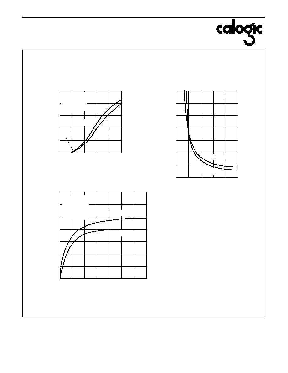
TYPICAL PERFORMANCE CHARACTERISTICS (T
A
= +25
o
C unless otherwise noted)
200
160
120
80
40
0
2.0
4.0
6.0
8.0
10
DS
µ
A
V = 10V
PULSE TEST
80 Sec
1% Duty Cycle
T = +25 C
o
A
T = +125 C
o
D'Z'
I 7.5mA
GS
D
(
on)
I -
O
N Dr
ai
n Cur
r
ent-
(
m
A
)
D
S(o
n
)
r
-D
r
a
i
n
-S
o
u
rc
e
ON
R
e
s
i
s
t
a
n
c
e
-(o
h
m
s
)
175
150
125
100
75
50
25
0
2.0
4.0
6.0
8.0
10
GS
I = 1.0mA
D
T = +125 C
o
T = +25 C
o
A
A
T = +125 C
o
T = +25 C
o
A
DS
µ
DRAIN-SOURCE ON RESISTANCE
-VS-
GATE-SOURCE VOLTAGE
35
30
25
20
15
10
5.0
0
10
20
30
40
50
60
70
D
fs
g -
F
or
w
a
r
d
T
r
ans
c
onduc
tanc
e-
(
mmhos
)
V -Gate-Source Voltage (Volts)
ON DRAIN CURRENT
-VS-
GATE-SOURCE VOLTAGE
V -Gate-Source Voltage (Volts)
A
V = 10V
f = 1KHz
PULSE TEST
80 Sec
1% Duty Cycle
I -Drain Current (mA)
FORWARD TRANSCONDUCTANCE
-VS-
ON DRAIN CURRENT