 | –≠–ª–µ–∫—Ç—Ä–æ–Ω–Ω—ã–π –∫–æ–º–ø–æ–Ω–µ–Ω—Ç: SST113-T1 | –°–∫–∞—á–∞—Ç—å:  PDF PDF  ZIP ZIP |

J/SST111 Series
Siliconix
S-52424--Rev. D, 14-Apr-97
1
N-Channel JFETs
J111
SST111
J112
SST112
J113
SST113
Product Summary
Part Number
V
GS(off)
(V)
r
DS(on)
Max (
W) I
D(off)
Typ (pA)
t
ON
Typ (ns)
J/SST111
≠3 to ≠10
30
5
4
J/SST112
≠1 to ≠5
50
5
4
J/SST113
v≠3
100
5
4
Features
Benefits
Applications
D Low On-Resistance: 111 < 30 W
D Fast Switching--t
ON
: 4 ns
D Low Leakage: 5 pA
D Low Capacitance: 3 pF
D Low Insertion Loss
D Low Error Voltage
D High-Speed Analog Circuit Performance
D Negligible "Off-Error," Excellent Accuracy
D Good Frequency Response, Low Glitches
D Eliminates Additional Buffering
D Analog Switches
D Choppers
D Sample-and-Hold
D Normally "On" Switches
D Current Limiters
Description
The J/SST111 series consists of all-purpose analog switches
designed to support a wide range of applications. The
J/SST113 are useful in a high-gain amplifier mode.
The J series, TO-226AA (TO-92) plastic package, provides
low cost, while the SST series, TO236 (SOT-23) package,
provides surface-mount capability. Both the J and SST series
are available in tape-and-reel for automated assembly (see
Packaging Information).
For similar products in TO-206AA(TO-18) packaging, see
the 2N/PN/SST4391 series, 2N4856A/4857A/4858A, and
2N5564/5565/5566 (duals) data sheets.
TO-226AA (TO-92)
Top View
J111
J112
J113
D
G
S
1
2
3
D
S
G
TO-236 (SOT-23)
2
3
1
Top View
SST111 (C1)*
SST112 (C2)*
SST113 (C3)*
*Marking Code for TO-236
Updates to this data sheet may be obtained via facsimile by calling Siliconix FaxBack, 1-408-970-5600. Please request FaxBack document #70232.
Applications information may also be obtained via FaxBack, request document #70598.
J/SST111 Series
2
Siliconix
S-52424--Rev. D, 14-Apr-97
Absolute Maximum Ratings
Gate-Drain, Gate-Source Voltage
≠35 V
. . . . . . . . . . . . . . . . . . . . . . . . . .
Gate Current
50 mA
. . . . . . . . . . . . . . . . . . . . . . . . . . . . . . . . . . . . . . . . . .
Lead Temperature (
1
/
16
" from case for 10 seconds)
300
_C
. . . . . . . . . .
Storage Temperature
≠55 to 150
_C
. . . . . . . . . . . . . . . . . . . . . . . . . . . . .
Operating Junction Temperature
≠55 to 150
_C
. . . . . . . . . . . . . . . . . . . .
Power Dissipation
a
(TO-236)
350 mW
. . . . . . . . . . . . . . . . . . . . . . . . .
(TO-226AA)
360 mW
. . . . . . . . . . . . . . . . . . . . . .
Notes
a.
Derate 2.8 mW/
_C above 25_C
Specifications
a
Limits
J/SST111
J/SST112
J/SST113
Parameter
Symbol
Test Conditions
Typ
b
Min
Max
Min
Max
Min
Max
Unit
Static
Gate-Source
Breakdown Voltage
V
(BR)GSS
I
G
= ≠1
mA , V
DS
= 0 V
≠55
≠35
≠35
≠35
V
Gate-Source Cutoff Voltage
V
GS(off)
V
DS
= 5 V, I
D
= 1
mA
≠3
≠10
≠1
≠5
≠3
Saturation Drain Current
c
I
DSS
V
DS
= 15 V, V
GS
= 0 V
20
5
2
mA
Gate Reverse Current
I
GSS
V
GS
= ≠15 V, V
DS
= 0 V
≠0.005
≠1
≠1
≠1
nA
Gate Reverse Current
I
GSS
T
A
= 125
_C
≠3
nA
Gate Operating Current
I
G
V
DG
= 15 V, I
D
= 10 mA
≠5
pA
Drain Cutoff Current
I
D(off)
V
DS
= 5 V, V
GS
=
-10 V
0.005
1
1
1
nA
Drain Cutoff Current
I
D(off)
T
A
= 125
_C
3
nA
Drain-Source On-Resistance
r
DS(on)
V
GS
= 0 V, V
DS
= 0.1 V
30
50
100
W
Gate-Source Forward Voltage
V
GS(F)
I
G
= 1 mA , V
DS
= 0 V
0.7
V
Dynamic
Common-Source Forward
Transconductance
g
fs
V
DS
= 20 V, I
D
= 1 mA
f
1 kH
6
mS
Common-Source
Output Conductance
g
os
DS
,
D
f = 1 kHz
25
mS
Drain-Source On-Resistance
r
ds(on)
V
GS
= 0 V, I
D
= 0 mA
f = 1 kHz
30
50
100
W
Common-Source
Input Capacitance
C
iss
V
DS
= 0 V, V
GS
=
-10 V
f
1 MH
7
12
12
12
pF
Common-Source Reverse
Transfer Capacitance
C
rss
DS
,
GS
f = 1 MHz
3
5
5
5
pF
Equivalent Input
Noise Voltage
e
n
V
DG
= 10 V, I
D
= 1 mA
f = 1 kHz
3
nV
/
Hz
Switching
Turn-On Time
t
d(on)
2
Turn-On Time
t
r
V
DD
= 10 V, V
GS(H)
= 0 V
S
S it hi
Ci
it
2
ns
Turn-Off Time
t
d(off)
GS( )
See Switching Circuit
6
ns
Turn-Off Time
t
f
15
Notes
a.
T
A
= 25
_C unless otherwise noted.
NCB
b.
Typical values are for DESIGN AID ONLY, not guaranteed nor subject to production testing.
c.
Pulse test: PW
v300 ms duty cycle v3%.
J/SST111 Series
Siliconix
S-52424--Rev. D, 14-Apr-97
3
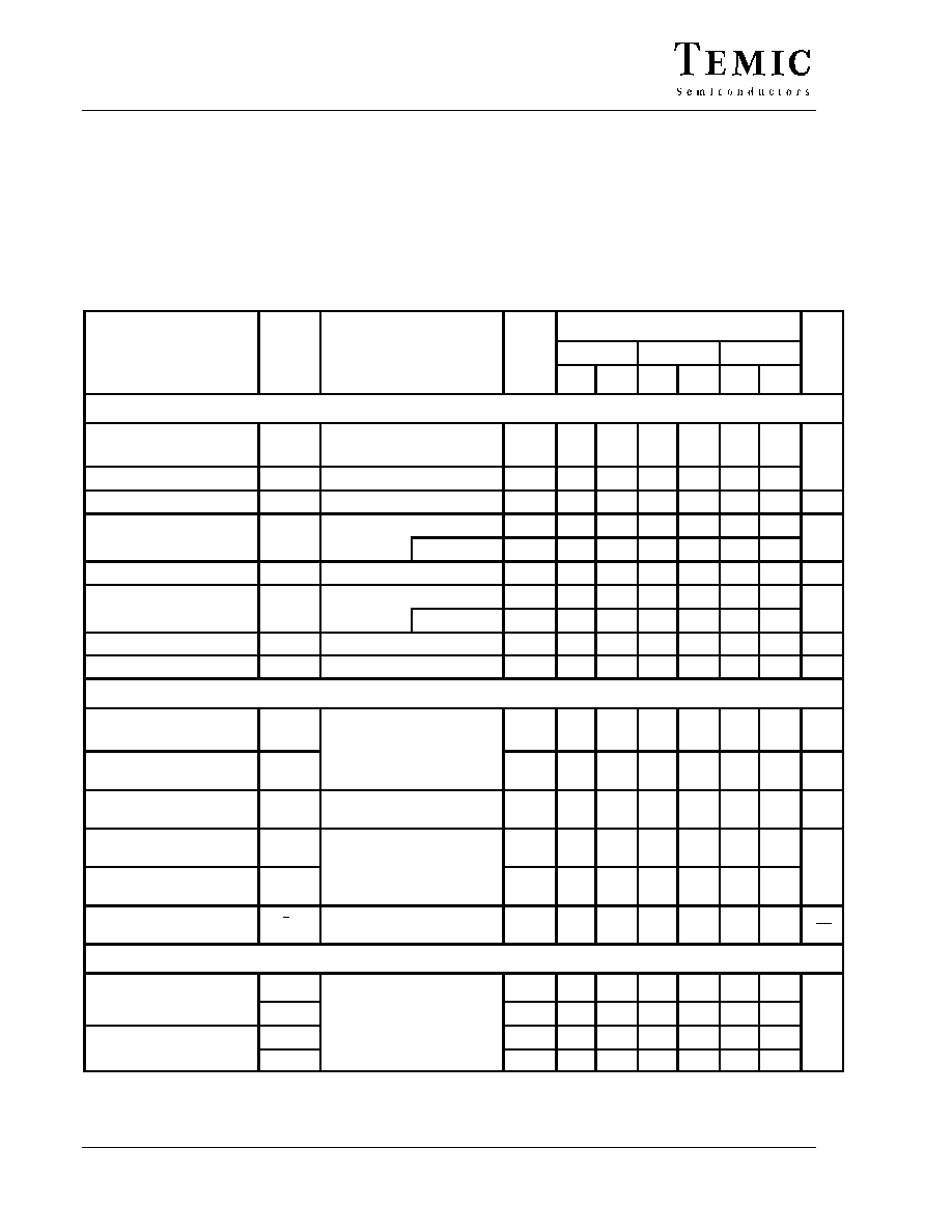
Typical Characteristics
160
120
On-Resistance and Drain Current
vs. Gate-Source Cutoff Voltage
On-Resistance vs. Drain Current
100
0
≠10
0
200
160
0
≠ Saturation Drain Current (mA)
I
DSS
r
DS
I
DSS
r
DS
@ I
D
= 1 mA, V
GS
= 0
I
DSS
@ V
DS
= 20 V, V
GS
= 0
100
0
1
10
100
V
GS(off)
= ≠2 V
≠4 V
≠8 V
T
A
= 25
_C
On-Resistance vs. Temperature
200
≠55
25
125
0
≠15
85
I
D
= 1 mA
r
DS
changes X 0.7%/
_C
V
GS(off)
= ≠2 V
≠4 V
≠8 V
Turn-On Switching
5
0
≠10
4
3
2
1
0
t
r
Switching T
ime
(ns)
t
d(on)
@
I
D
= 3 mA
t
d(on)
@
I
D
= 12 mA
t
r
approximately independent of I
D
V
DD
= 5 V, R
G
= 50
W
V
GS(L)
= ≠10 V
Turn-Off Switching
30
0
10
24
18
12
6
0
t
f
@
V
GS(off)
= ≠2 V
t
f
@
V
GS(off)
= ≠8 V
t
d(off)
t
d(off)
independent of device V
GS(off)
V
DD
= 5 V, V
GS(L)
= ≠10 V
Capacitance vs. Gate-Source Voltage
30
≠20
24
18
12
6
0
Capacitance (pF)
f = 1 MHz
C
iss
@ V
DS
= 0 V
C
rss
@ V
DS
= 0 V
0
V
GS(off)
≠ Gate-Source Cutoff Voltage (V)
T
A
≠ Temperature (
_C)
V
GS
≠ Gate-Source Voltage (V)
V
GS(off)
≠ Gate-Source Cutoff Voltage (V)
I
D
≠ Drain Current (mA)
I
D
≠ Drain Current (mA)
80
60
40
20
80
40
80
60
40
20
≠2
≠4
≠6
≠8
≠35
120
80
40
5
45
65
105
≠2
≠4
≠6
≠8
2
4
6
8
≠4
≠8
≠12
≠16
Switching T
ime
(ns)
r
DS(on)
≠ Drain-Source On-Resistance (
)
W
r
DS(on)
≠ Drain-Source On-Resistance (
)
W
r
DS(on)
≠ Drain-Source On-Resistance (
)
W
J/SST111 Series
4
Siliconix
S-52424--Rev. D, 14-Apr-97
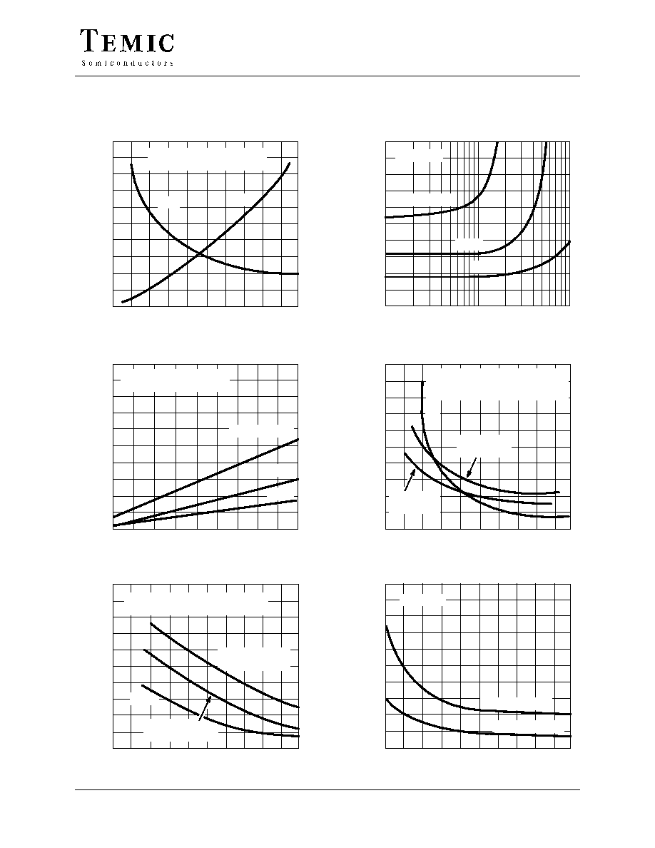
Typical Characteristics (Cont'd)
1 pA
Noise Voltage vs. Frequency
100
10
1
10
100
1 k
100 k
10 k
I
D
= 10 mA
Forward Transconductance and Output Conductance
vs. Gate-Source Cutoff Voltage
50
0
0
≠2
≠10
500
250
0
g
fs
≠ Forward
T
ransconductance
(mS)
S)
g
os
≠ Output Conductance (
m
g
fs
g
os
g
fs
and g
os
@ V
DS
= 20 V
V
GS
= 0 V, f = 1 kHz
Gate Leakage Current
0
30
1 nA
100 pA
10 pA
0.1 pA
≠ Gate Leakage
I
G
T
A
= 125
_C
T
A
= 25
_C
1 mA
I
GSS
@ 25
_C
10 nA
I
D
= 10 mA
Common-Gate Input Admittance
100
10
1
0.1
100
1000
200
500
(mS)
g
ig
b
ig
V
DG
= 10 V
I
D
= 10 mA
T
A
= 25
_C
Common-Gate Forward Admittance
Common-Gate Reverse Admittance
100
10
1
0.1
100
1000
200
500
(mS)
≠g
fg
b
fg
g
fg
V
DG
= 10 V
I
D
= 10 mA
T
A
= 25
_C
10
1.0
0.1
0.01
100
1000
200
500
V
DG
= 10 V
I
D
= 10 mA
T
A
= 25
_C
≠g
rg
≠b
rg
+g
rg
(mS)
V
DG
≠ Drain-Gate Voltage (V)
V
GS(off)
≠ Gate-Source Cutoff Voltage (V)
f ≠ Frequency (Hz)
f ≠ Frequency (MHz)
f ≠ Frequency (MHz)
f ≠ Frequency (MHz)
40
30
20
10
≠4
≠6
≠8
I
GSS
@ 125
_C
10 mA
1 mA
6
12
18
24
V
DS
= 10 V
I
D
= 1 mA
nV
e
n
/
Hz
)
(
≠ Noise
V
oltage
J/SST111 Series
Siliconix
S-52424--Rev. D, 14-Apr-97
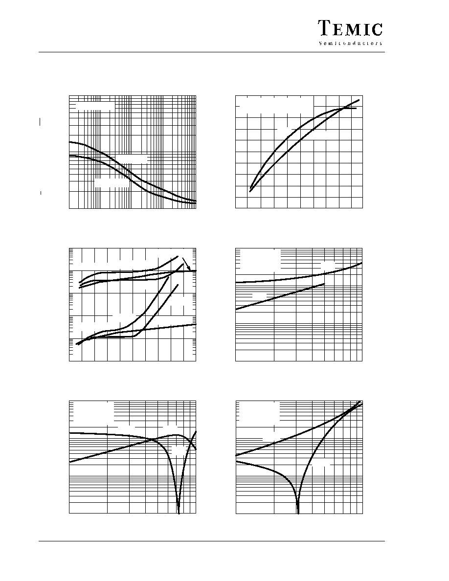
5
Typical Characteristics (Cont'd)
≠ Drain Current (mA)
I
D
Output Characteristics
100
0
10
80
60
40
20
0
V
DS
≠ Drain-Source Voltage (V)
2
4
6
8
Common-Gate Output Admittance
100
10
1
0.1
100
1000
200
500
(mS)
V
DG
= 10 V
I
D
= 10 mA
T
A
= 25
_C
f ≠ Frequency (MHz)
≠ Drain Current (mA)
I
D
Output Characteristics
40
0
1.0
32
24
16
8
0
V
DS
≠ Drain-Source Voltage (V)
0.2
0.4
0.6
0.8
≠ Drain Current (mA)
I
D
Transfer Characteristics
100
0
≠5
80
60
40
20
0
V
GS
≠ Gate-Source Voltage (V)
≠1
≠2
≠3
≠4
g
og
b
og
V
GS
= 0 V
≠0.5
≠1.0
≠1.5
≠2.0
≠2.5
V
GS(off)
= ≠4 V
V
GS(off)
= ≠4 V
V
GS
= 0 V
≠0.5
≠1.0
≠1.5
≠2.0
≠2.5
≠3.0
V
GS(off)
= ≠4 V
T
A
= ≠55
_C
25
_C
125
_C
V
DS
= 20 V
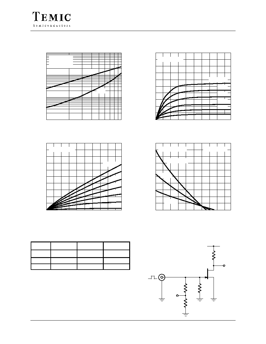
Switching Time Test Circuit
J/SST111
J/SST112
J/SST113
V
GS(L)
≠12 V
≠7 V
≠5 V
R
L
*
800
W
1600
W
3200
W
I
D(on)
12 mA
6 mA
3 mA
*Non-inductive
Input Pulse
Sampling Scope
Rise Time < 1 ns
Fall Time < 1 ns
Pulse Width 100 ns
PRF 1 MHz
Rise Time 0.4 ns
Input Resistance 10 M
W
Input Capacitance 1.5 pF
51
W
51
W
1 k
W
V
GS
Scope
V
DD
R
L
OUT
V
GS(H)
V
GS(L)