
N-Channel JFET
Monolithic Dual
SST440 / SST441
FEATURES
∑
∑
High Gain . . . . . . . . . . . . . . . . . . . . . . . gf
s
> 6 mS typical
∑
∑
Low Leakage . . . . . . . . . . . . . . . . . . . . . . I
G
< 1pA typical
∑
∑
Low Noise
∑
∑
Surface Mount Package
APPLICATIONS
∑
∑
Differential Wideband Amplifiers
∑
∑
VHF/UHF Amplifiers
∑
∑
Test and Measurement
DESCRIPTION
Calogic's SST440 Series is a high speed N-Channel
Monolithic Dual JFET in a surface mount SO-8 package. This
device is well suited for use as wideband differential amplifiers
in test and measurement applications. The combination of
high gain, low leakage and low noise make it an excellent
performer.
ORDERING INFORMATION
Part
Package
Temperature Range
SST440-1
Plastic SO-8
-55
o
C to +150
o
C
NOTE: For Sorted Chips in Carriers, See U440 Series
PIN CONFIGURATION
CORPORATION
SO-8
TOP VIEW
(1) S1
(2) D1
(3) G1
(4) N/C
N/C (8)
G2 (7)
D2 (6)
S2 (5)
CJ1
PRODUCT MARKING
SST440
SST440
SST441
SST441
SST440 / SST441
CORPORATION
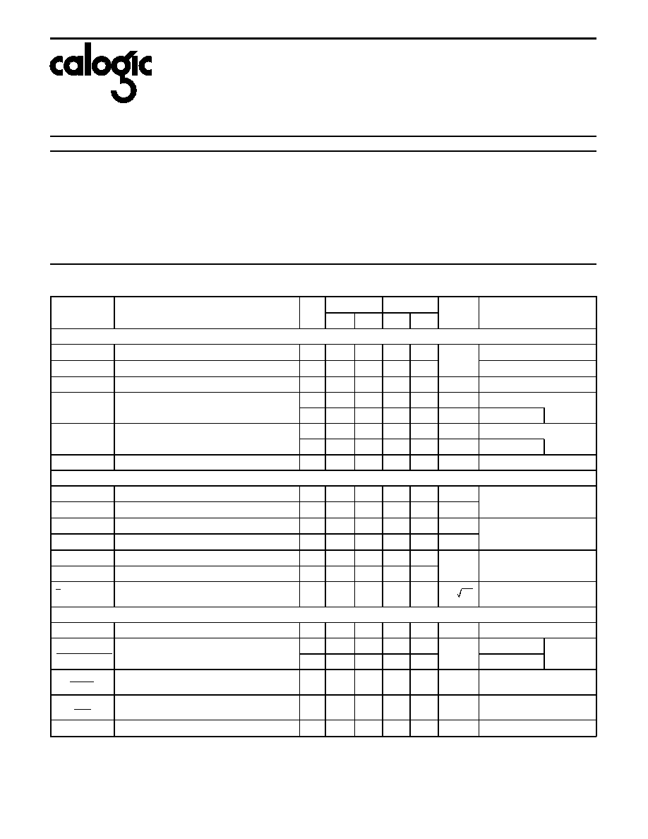
ABSOLUTE MAXIMUM RATINGS (T
A
= 25
o
C unless otherwise noted)
Parameter/Test Condition
Symbol
Limit
Unit
Gate-Drain Voltage
V
GD
-25
V
Gate-Source Voltage
V
GS
-25
V
Forward Gate Current
I
G
50
mA
Power Dissipation
(per side)
P
D
300
mW
(total)
500
mW
Power Derating
(per side)
2.4
mW/
o
C
(total)
4
mW/
o
C
Operating Junction Temperature
T
J
-55 to 150
o
C
Storage Temperature
T
stg
-55 to 150
o
C
Lead Temperature (1/16" from case for 10 seconds)
T
L
300
o
C
ELECTRICAL CHARACTERISTICS (T
A
= 25
o
C unless otherwise noted)
SYMBOL
CHARACTERISTCS
TYP
1
SST440
SST441
UNIT
TEST CONDITIONS
MIN
MAX
MIN
MAX
STATIC
V
(BR)GSS
Gate-Source Breakdown Voltage
-35
-25
-25
V
I
G
= -1
µ
A, V
DS
= 0V
V
GS(OFF
)
Gate-Source Cut off Voltage
-3.5
-1
-6
-1
-6
V
DS
= 10V, I
D
= 1nA
I
DSS
Saturation Drain Current
2
15
6
30
6
30
mA
V
DS
= 10V, V
GS
= 0V
I
GSS
Gate Reverse Current
-1
-500
-500
pA
V
GS
= -15V, V
DS
= 0V
-0.2
nA
T
A
= 125
o
C
I
G
Gate Operating Current
-1
-500
-500
pA
V
DG
= 10V, I
D
= 5mA
-0.2
nA
T
A
= 125
o
C
V
GS(F)
Gate-Source Forward Voltage
0.7
V
I
G
= 1mA, V
DS
= 0V
DYNAMIC
g
fs
Common-Source Forward Transconductance
6
4.5
9
4.5
9
mS
V
DG
= 10V, I
D
= 5mA
f = 1kHz
g
os
Common-Source Output Conductance
20
200
200
µ
S
g
fs
Common-Source Forward Transconductance
5.5
mS
V
DG
= 10V, I
D
= 5mA
f = 100MHz
g
os
Common-Source Output Conductance
30
µ
S
C
iss
Common-Source Input Capacitance
3.5
pF
V
DG
= 10V, I
D
= 5mA
f = 1MHz
C
rss
Common-Source Reverse Transfer Capacitance
1
e
n
Equivalent Input Noise Voltage
4
nV/ Hz
V
DG
= 10V, I
D
= 5mA
f = 10kHz
MATCHING
| V
GS1
-V
GS2
|
Differential Gate-Source Voltage
7
10
20
mV
V
DG
= 10V, I
D
= 5mA
| V
GS1
-V
GS2
|
T
Gate-Source Voltage Differential Change with
Temperature
10
µ
V/
o
C
T = -55 to 25
o
C
V
DG
=10V,
I
D
= 5mA
10
T = 25 to 125
o
C
I
DSS1
I
DSS2
Saturation Drain Current Ratio
0.98
V
DS
= 10V, V
GS
= 0V
g
fs1
g
fs2
Transconductance Ratio
0.98
V
DG
= 10V, I
D
= 5mA
f= 1 kHz
CMRR
Common Mode Rejection Ratio
90
dB
V
DD
= 5 to 10V, I
D
= 5mA
NOTES: 1. For design aid only, not subject to production testing.
2. Pulse test; PW = 300
µ
s, duty cycle
3%.