N-Channel JFET
Monolithic Dual
U443 / U444
FEATURES
∑
∑
High Gain . . . . . . . . . . . . . . . . . . . . . . . g
fs
> 6 mS typical
∑
∑
Low Leakage . . . . . . . . . . . . . . . . . . . . . . I
G
< 1pA typical
∑
∑
Low Noise
APPLICATIONS
∑
∑
Differential Wideband Amplifiers
∑
∑
VHF/UHF Amplifiers
∑
∑
Test and Measurement
∑
∑
Multi-Chip/Hybrids
DESCRIPTION
The U443 Series is an N-Channel Monolithic Dual JFET
designed for high speed amplifier circuits. Featuring high gain
( > 6 mS typical), low leakage (< 1pA typical) and low noise
this device is an excellent choice for high performance test
and measurement, wideband amplifiers and VHF/UHF
circuits.
ORDERING INFORMATION
Part
Package
Temperature Range
U443-4
Hermetic M0-002AG (TO-78) -55
o
C to +150
o
C
XU443-4 Sorted Chips in Carriers
-55
o
C to +150
o
C
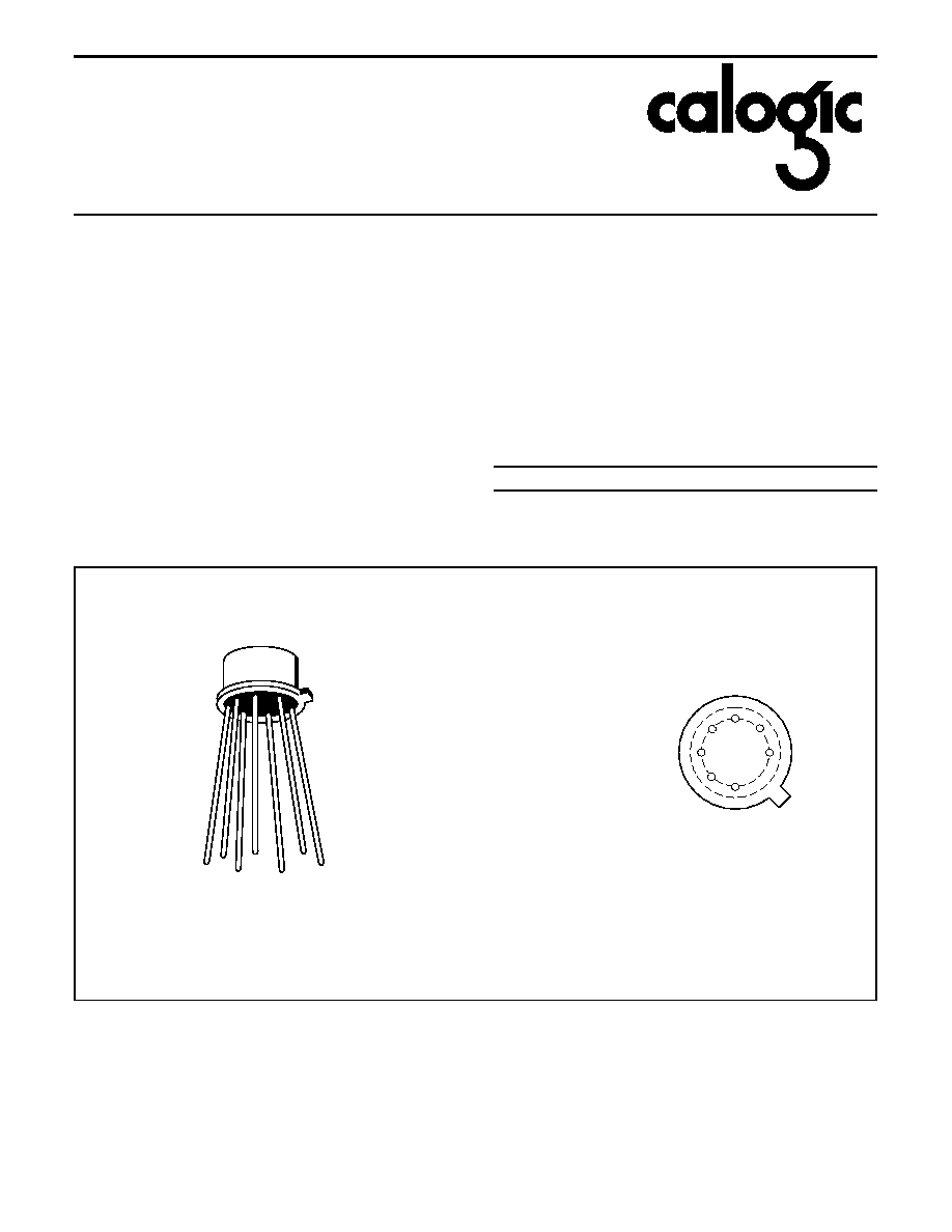
PIN CONFIGURATION
CORPORATION
S2
G1
D2
D1
G2
S1
C
TO-78
1
2
3
4 5
BOTTOM VIEW
1
2
3
4
5
6
7
7
6
SOURCE 1
DRAIN 1
GATE 1
CASE/BODY
SOURCE 2
DRAIN 2
GATE 2
CJ1
U443 / U444
CORPORATION
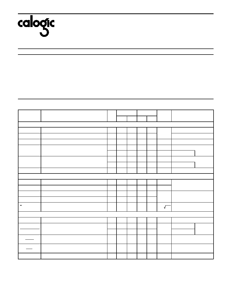
ABSOLUTE MAXIMUM RATINGS (T
A
= 25
o
C unless otherwise noted)
Parameter/Test Condition
Symbol
Limit
Unit
Gate-Drain Voltage
V
GD
-25
V
Gate-Source Voltage
V
GS
-25
V
Gate-Gate Voltage
V
GG
±
50
V
Forward Gate Current
I
G
50
mA
Power Dissipation
(per side)
P
D
367
mW
(total)
500
mW
Power Derating
(per side)
3
mW/
o
C
(total)
4
mW/
o
C
Operating Junction Temperature
T
J
-55 to 150
o
C
Storage Temperature
T
stg
-65 to 200
o
C
Lead Temperature (1/16" from case for 10 seconds)
T
L
300
o
C
ELECTRICAL CHARACTERISTICS (T
A
= 25
o
C unless otherwise noted)
SYMBOL
CHARACTERISTCS
TYP
1
U443
U444
UNIT
TEST CONDITIONS
MIN
MAX
MIN
MAX
STATIC
V
(BR)GSS
Gate-Source Breakdown Voltage
-35
-25
-25
V
I
G
= -1
µ
A, V
DS
= 0V
V
GS(OFF
)
Gate-Source Cut off Voltage
-3.5
-1
-6
-1
-6
V
DS
= 10V, I
D
= 1nA
I
DSS
Saturation Drain Current
2
15
6
30
6
30
mA
V
DS
= 10V, V
GS
= 0V
I
GSS
Gate Reverse Current
-1
-500
-500
pA
V
GS
= -15V, V
DS
= 0V
-2
nA
T
A
= 150
o
C
I
G
Gate Operating Current
-1
-500
-500
pA
V
DG
= 10V, I
D
= 5mA
-0.3
nA
T
A
= 125
o
C
V
GS(F)
Gate-Source Forward Voltage
0.7
V
I
G
= 1mA, V
DS
= 0V
DYNAMIC
g
fs
Common-Source Forward Transconductance
6
4.5
9
4.5
9
mS
V
DG
= 10V, I
D
= 5mA
f = 1kHz
g
os
Common-Source Output Conductance
70
200
200
µ
S
C
iss
Common-Source Input Capacitance
3
pF
V
DG
= 10V, I
D
= 5mA
f = 1MHz
C
rss
Common-Source Reverse Transfer Capacitance
1
e
n
Equivalent Input Noise Voltage
4
nV/ Hz
V
DG
= 10V, I
D
= 5mA
f = 10kHz
MATCHING
| V
GS1
-V
GS2
|
Differential Gate-Source Voltage
6
10
20
mV
V
DG
= 10V, I
D
= 5mA
| V
GS1
-V
GS2
|
T
Gate-Source Voltage Differential Change with
Temperature
20
µ
V/
o
C
T = -55 to 25
o
C
V
DG
=10V,
I
D
= 5mA
20
T = 25 to 125
o
C
I
DSS1
I
DSS2
Saturation Drain Current Ratio
0.97
V
DS
= 10V, V
GS
= 0V
g
fs1
g
fs2
Transconductance Ratio
0.97
V
DG
= 10V, I
D
= 5mA
f= 1 kHz
CMRR
Common Mode Rejection Ratio
85
dB
V
DD
= 5 to 10V, I
D
= 5mA
NOTES: 1. For design aid only, not subject to production testing.
2. Pulse test; PW = 300
µ
s, duty cycle
3%.