N-Channel JFET
Low Noise Amplifier
2N4338 ≠ 2N4341
FEATURES
∑
∑
Exceptionally High Figure of Merit
∑
∑
Radiation Immunity
∑
∑
Extremely Low Noise and Capacitance
∑
∑
High Input Impedance
APPLICATIONS
∑
∑
Low-level Choppers
∑
∑
Data Switches
∑
∑
Multiplexers and Low Noise Amplifiers
ABSOLUTE MAXIMUM RATINGS
(T
A
= 25
o
C unless otherwise noted)
Gate-Source or Gate-Drain Voltage . . . . . . . . . . . . . . . . -50V
Gate Current . . . . . . . . . . . . . . . . . . . . . . . . . . . . . . . . . 50mA
Storage Temperature Range . . . . . . . . . . . . . -65
o
C to +200
o
C
Operating Temperature Range . . . . . . . . . . . -55
o
C to +175
o
C
Lead Temperature (Soldering, 10sec) . . . . . . . . . . . . . +300
o
C
Power Dissipation . . . . . . . . . . . . . . . . . . . . . . . . . . . . 300mW
Derate
above
25
o
C . . . . . . . . . . . . . . . . . . . . . . . 2.0mW/
o
C
NOTE: Stresses above those listed under "Absolute Maximum
Ratings" may cause permanent damage to the device. These are
stress ratings only and functional operation of the device at these or
any other conditions above those indicated in the operational sections
of the specifications is not implied. Exposure to absolute maximum
rating conditions for extended periods may affect device reliability.
ORDERING INFORMATION
Part
Package
Temperature Range
2N4338-41
Hermetic TO-18
-55
o
C to +175
o
C
X2N4338-41
Sorted Chips in Carriers
-55
o
C to +175
o
C
CORPORATION
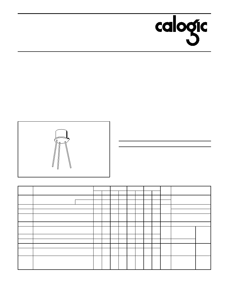
PIN CONFIGURATION
S
TO-18
G,C
D
ELECTRICAL CHARACTERISTICS (T
A
= 25
o
C unless otherwise specified)
SYMBOL
PARAMETER
2N4338
2N4339
2N4340
2N4341
UNITS
TEST CONDITIONS
MIN MAX MIN MAX MIN MAX MIN MAX
I
GSS
Gate Reverse Current
-0.1
-0.1
-0.1
-0.1
nA
V
GS
= -30V, V
DS
= 0
T
A
= 150
o
C
-0.1
-0.1
-0.1
-0.1
µ
A
BV
GSS
Gate-Source Breakdown Voltage
-50
-50
-50
-50
V
I
G
= -1
µ
A, V
DS
= 0
V
GS(off)
Gate-Source Cutoff Voltage
-0.3
-1
-0.6
-1.8
-1
-3
-2
-6
V
DS
= 15V, I
D
= 0.1
µ
A
I
D(off)
Drain Cutoff Current
0.05
(-5)
0.05
(-5)
0.05
(-5)
0.07
(-10)
nA
(V)
V
DS
= 15V,
V
GS
= ( )
I
DSS
Saturation Drain Current (Note 2)
0.2
0.6
0.5
1.5
1.2
3.6
3
9
mA
V
DS
= 15V, V
GS
= 0
g
fs
Common-Source Forward
Transconductance (Note 2)
600 1800 800 2400 1300 3000 2000 4000
µ
S
V
DS
= 15V,
V
GS
= 0
f = 1kHz
g
os
Common-Source Output Conductance
5
15
30
60
r
DS(on)
Drain-Source ON Resistance
2500
1700
1500
800
ohm
V
DS
= 0, I
DS
= 0
C
iss
Common-Source Input Capacitance
7
7
7
7
pF
V
DS
= 15V,
V
GS
= 0 (Note 1)
f = 1MHz
C
rss
Common-Source Reverse Transfer
Capacitance
3
3
3
3
NF
Noise Figure (Note 1)
1
1
1
1
dB
V
DS
= 15V,
V
GS
= 0
R
gen
= 1meg,
BW = 200Hz
f = 1kHz
NOTES: 1. For design reference only, not 100% tested.
2. Pulse test duration 2ms (non-JEDEC Condition).
5010