Dual N-Channel JFET Switch
U401 ≠ U406
FEATURES
∑
∑
Minimum System Error and Calibration
∑
∑
Low Drift With Temperature
∑
∑
Operates From Low Power Supply Voltages
∑
∑
High Output Impedance
ABSOLUTE MAXIMUM RATINGS
(T
A
= 25
o
C unless otherwise specified)
Gate-Drain or Gate-Source Voltage . . . . . . . . . . . . . . . . . 50V
Gate Current (Note 1) . . . . . . . . . . . . . . . . . . . . . . . . . . 10mA
Storage Temperature Range . . . . . . . . . . . . . -65
o
C to +200
o
C
Operating Temperature Range . . . . . . . . . . . -55
o
C to +150
o
C
Lead Temperature (Soldering, 10sec) . . . . . . . . . . . . . +300
o
C
One Side
Both Sides
Power Dissipation (T
A
= 85
o
C)
300mW
500mW
Derate
above
25
o
C
2.6mW/
o
C
5mW/
o
C
NOTE: Stresses above those listed under "Absolute Maximum
Ratings" may cause permanent damage to the device. These are
stress ratings only and functional operation of the device at these or
any other conditions above those indicated in the operational sections
of the specifications is not implied. Exposure to absolute maximum
rating conditions for extended periods may affect device reliability.
ORDERING INFORMATION
Part
Package
Temperature Range
U401-6
Hermetic TO-71
-55
o
C to +150
o
C
XU401-6
Sorted Chips in Carriers
-55
o
C to +150
o
C
CORPORATION
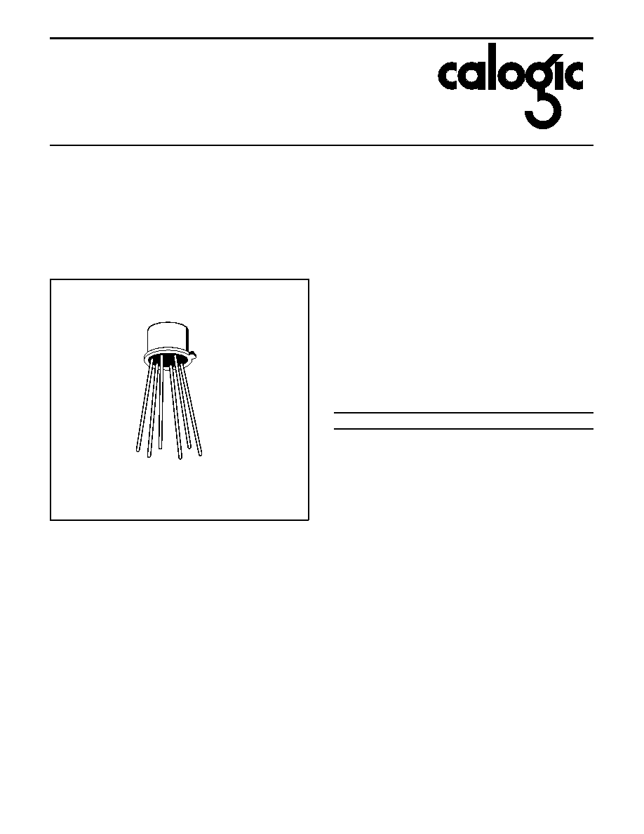
PIN CONFIGURATION
S2
G1
D2
D1
G2
S1
TO-71
CJ2
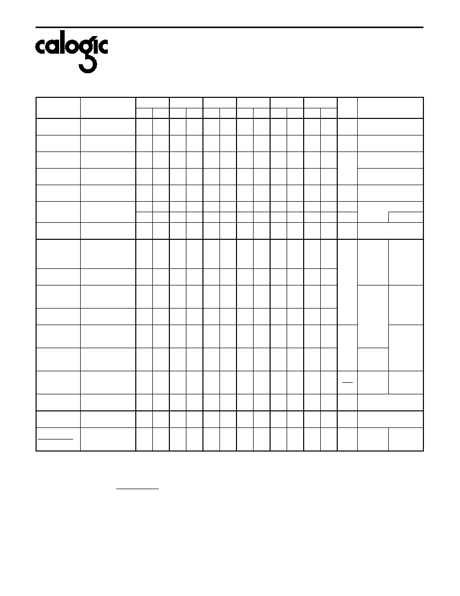
ELECTRICAL CHARACTERISTICS (T
A
= 25
o
C unless otherwise specified)
SYMBOL
PARAMETER
U401
U402
U403
U404
U405
U406
UNITS
TEST CONDITIONS
MIN
MAX
MIN
MAX
MIN
MAX
MIN
MAX
MIN
MAX
MIN
MAX
BV
GSS
Gate-Source
Breakdown Voltage
-50
-50
-50
-50
-50
-50
V
V
DS
= 0, I
G
= -1
µ
A
I
GSS
Gate Reverse Current
(Note 2)
-25
-25
-25
-25
-25
-25
pA
V
DS
= 0, V
GS
= -30V
V
GS(off)
Gate-Source Cutoff
Voltage
-.5
-2.5
-.5
-2.5
-.5
-2.5
-.5
-2.5
-.5
-2.5
-.5
-2.5
V
V
DS
= 15V, I
D
= 1nA
V
GS(on)
Gate-Source Voltage
(on)
-2.3
-2.3
-2.3
-2.3
-2.3
-2.3
V
DG
= 15V, I
D
= 200
µ
A
I
DSS
Saturation Drain
Current (Note 3)
0.5
10.0
0.5
10.0
0.5
10.0
0.5
10.0
0.5
10.0
0.5
10.0
mA
V
DS
= 10V, V
GS
= 0
I
G
Operating Gate
Current (Note 2)
-15
-15
-15
-15
-15
-15
pA
V
DG
= 15V, I
D
= 200
µ
A
-10
-10
-10
-10
-10
-10
nA
T
A
= 125
o
C
BV
G1-G2
Gate-Gate
Breakdown Voltage
±
50
±
50
±
50
±
50
±
50
±
50
V
V
DS
= 0, V
GS
= 0,
I
G
=
±
1
µ
A
g
fs
Common-Source
Forward
Transconductance
(Note 3)
2000
7000
2000
7000
2000
7000
2000
7000
2000
7000
2000
7000
µ
S
V
DS
= 10V,
V
GS
= 0
f = 1kHz
g
os
Common-Source
Output Conductance
20
20
20
20
20
20
g
fs
Common-Source
Forward
Transconductance
1000
2000
1000
2000
1000
2000
1000
2000
1000
2000
1000
2000
V
DG
= 15V,
I
D
= 200
µ
A
f = 1kHz
g
os
Common-Source
Output Conductance
2.0
2.0
2.0
2.0
2.0
2.0
C
iss
Common-Source
Input Capacitance
(Note 6)
8.0
8.0
8.0
8.0
8.0
8.0
pF
f = 1MHz
C
rss
Common-Source
Reverse Transfer
Capacitance (Note 6)
3.0
3.0
3.0
3.0
3.0
3.0
e
n
Equivalent
Short-Circuit Input
Noise Voltage
20
20
20
20
20
20
nV
Hz
V
DS
= 15V,
V
GS
= 0
f = 10Hz
(Note 6)
CMRR
Common-Mode
Rejection Ratio
95
95
95
95
90
dB
V
DG
= 10 to 20V,
I
D
= 200
µ
A (Note 5, 6)
|
V
GS1
-
V
GS2
|
Differential
Gate-Source Voltage
5
10
10
15
20
40
mV
V
DG
= 10V, I
D
= 200
µ
A
|
V
GS1
-
V
GS2
|
T
Gate-Source Voltage
Differential Drift (Note
4)
10
10
25
25
40
80
µ
V/
o
C
V
DG
= 10V,
I
D
= 200
µ
A
T
A
= -55
o
C
T
B
= +25
o
C
T
C
= +125
o
C
NOTES: 1. Per transistor.
2. Approximately doubles for every 10
o
C increase in T
A
.
3. Pulse test duration = 300
µ
s; duty cycle
3%.
4. Measured at end points T
A
, T
B
, T
C
.
5. CMRR = 20 log
10
V
DD
|
V
GS
1
-
V
GS
2
|
,
V
DD
= 10V.
6. For design reference only, not 100% tested.
U401 ≠ U406
CORPORATION