4
3
2
26
INVERTING INPUT
DIRECT INPUT
OFFSET ADJUST
REFERENCE HOLD
27
32, 33
7, 35, 37
DATA VALID
DIGITAL GROUND
ANALOG GROUND
25
23
10
24
6
START CONVERT
BIT 1 (MSB)
BIT 14 (LSB)
OUT-OF-RANGE
+2.4V REFERENCE OUTPUT
+12V
A
≠5V
A
+5V
A
+5V
D
39
38
36
34
TIMING
AND
CONTROL
SAMPLING
A/D
NON-INVERTING INPUT
75
9
523
9
0.01µF
5K
9
1
FINE GAIN ADJUST
5
INPUT AMPLIFIER
30 31
A1
CORRELATED
DOUBLE
SAMPLER
Aÿ
FEATURES
∑
14-bit resolution
∑
3MPPS throughput rate (14-bits)
∑
Functionally complete
∑
Very low noise
∑
Excellent Signal-to-Noise ratio
∑
Edge triggered
∑
Small, 40-pin, TDIP package
∑
Low power, 500mW typical
∑
Low cost
∑
Programmable Analog Bandwidth
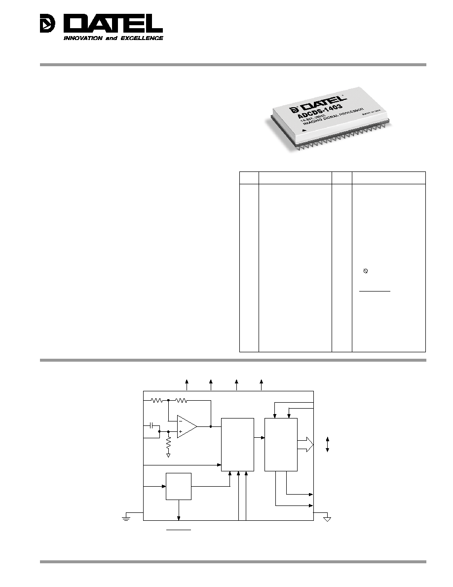
GENERAL DESCRIPTION
The ADCDS-1403 is an application-specific video signal
processor designed for electronic-imaging applications that
employ CCD's (charge coupled devices) as their
photodetector. The ADCDS-1403 incorporates a "user
configurable" input amplifier, a CDS (correlated double
sampler) and a sampling A/D converter in a single package,
providing the user with a complete, high performance, low-
cost, low-power, integrated solution.
The key to the ADCDS-1403's performance is a unique, high-
speed, high-accuracy CDS circuit, which eliminates the
effects of residual charge, charge injection and "kT/C" noise
on the CCD's output floating capacitor, producing a "valid
video" output signal. The ADCDS-1403 digitizes this resultant
"valid video" signal using a high-speed, low-noise sampling
A/D converter.
The ADCDS-1403 requires only the rising edge of start
convert pulse to initiate its conversion process. Additional
features of the ADCDS-1403 include gain adjust, offset
adjust, precision +2.4V reference, and a programmable
analog bandwidth function.
Figure 1. ADCDS-1403 Functional Block Diagram
1
FINE GAIN ADJUST
40
NO CONNECT
2
OFFSET ADJUST
39
+12V
3
DIRECT INPUT
38
≠5VA
4
INVERTING INPUT
37
ANALOG GROUND
5
NON-INVERTING INPUT
36
+5VA
6
+2.4V REF. OUTPUT
35
ANALOG GROUND
7
ANALOG GROUND
34
+5VD
8
NO CONNECT
33
DIGITAL GROUND
9
NO CONNECT
32
DIGITAL GROUND
10
BIT 14 (LSB)
31
A1
11
BIT 13
30
A
12
BIT 12
29
NO CONNECT
13
BIT 11
28
NO CONNECT
14
BIT 10
27
DATA VALID
15
BIT 9
26
REFERENCE HOLD
16
BIT 8
25
START CONVERT
17
BIT 7
24
OUT-OF-RANGE
18
BIT 6
23
BIT 1 (MSB)
19
BIT 5
22
BIT 2
20
BIT 4
21
BIT 3
INPUT/OUTPUT CONNECTIONS
PIN
FUNCTION
PIN
FUNCTION
Æ
Æ
DATEL, Inc., Mansfield, MA 02048 (USA)
∑
Tel: (508) 339-3000, (800) 233-2765 Fax: (508) 339-6356
∑
Email: sales@datel.com
∑
Internet: www.datel.com
ADCDS-1403
14-Bit, 3 Megapixels/Second
Imaging Signal Processor

ADCDS-1403
2
Æ
Æ
ANALOG INPUT
MIN.
TYP.
MAX.
UNITS
Input Voltage Range
(externally configurable)
0.350
2.8
--
Volts p-p
Input Resistance
--
5000
--
Ohm
Input Capacitance
--
10
--
pF
DIGITAL INPUTS
Logic Levels
Logic 1
+3.5
--
--
Volts
Logic 0
--
--
+.80
Volts
Logic Loading
Logic 1
--
--
+10
uA
Logic 0
--
--
≠10
uA
DIGITAL OUTPUTS
Logic Levels
Logic 1 (IOH = .5ma)
+2.4
--
--
Volts
Logic 1 (IOH = 50µa)
+4.5
--
--
Volts
Logic 0 (IOL = 1.6ma)
--
--
+0.4
Volts
Logic 0 (IOL = 50ua)
--
--
+0.1
Volts
Internal Reference
Voltage
(Fine gain adjust pin (1) grounded)
+25∞C
2.35
2.4
2.45
Volts
0 to 70∞C
2.35
2.4
2.45
Volts
≠55 to +125∞C
2.35
2.4
2.45
Volts
External Current
--
1.0
--
mA
STATIC PERFORMANCE
Differential Nonlinearity
(Histogram, 98kHz) +25∞C
≠0.90
±0.5
+.90
LSB
0 to 70∞C
≠0.90
±0.5
+.90
LSB
≠55 to +125∞C
≠1.0
±0.6
+1.0
LSB
Integral Nonlinearity
+25∞C
--
±2.5
--
LSB
0 to 70∞C
--
±2.5
--
LSB
≠55 to +125∞C
--
±2.5
--
LSB
Guaranteed No Missing Codes
0 to 70∞C
14
--
--
LSB
≠55 to +125∞C
14
--
--
LSB
DC Noise
+25∞C
--
1.0
1.6
LSB
0 to 70∞C
--
1.0
2.0
LSB
≠55 to +125∞C
--
1.25
2.5
LSB
Offset Error
+25∞C
--
±0.6
±1.25
%FSR
0 to 70∞C
--
±0.6
±1.25
%FSR
≠55 to +125∞C
--
±0.6
±1.45
%FSR
Gain Error
+25∞C
--
±1.00
±2.8
%FSR
0 to 70∞C
--
±1.35
±2.8
%FSR
≠55 to +125∞C
--
±1.35
±2.8
%FSR
PARAMETERS
MIN.
TYP.
MAX.
UNITS
+12V Supply (Pin 32)
0
--
+14
Volts
≠5V Supply (Pin 31)
≠0.3
--
+6.5
Volts
+5V Supply (Pin 28, 29)
0
--
≠6.5
Volts
Digital Input (Pin 23, 24)
≠0.3
--
Vdd+0.3V
Volts
Analog Input (Pin 3,4,5)
≠5
--
+5
Volts
Lead Temperature (10 seconds)
--
--
300
∞ C
ABSOLUTE MAXIMUM RATINGS
FUNCTIONAL SPECIFICATIONS
T
he following specifications apply over the operating temperature range, under the following conditions:
Vcc=+12V, +Vdd=+5V, Vee=≠5V, fin=98KHz, sample rate=3MHz.
DYNAMIC PERFORMANCE
MIN.
TYP.
MAX.
UNITS
Reference Hold
Aquisition Time
100
--
--
ns
Droop
@ +25∞C
--
25
--
mV/us
@ ≠55 to +125∞C
--
100
--
mV/us
Peak Harmonic (SFDR)
(CDD-IN, input on pin (3)
Input @ 98kHz)
@ +25 ∞C
--
≠76
--
dB
@ 0 to +70∞C
--
≠76
--
dB
@ ≠55 to +125∞C
--
≠74
--
dB
Peak Harmonic (SFDR)
(Input on pin (5)
Input @ 98kHz)
@ +25 ∞C
--
≠76
--
dB
@ 0 to +70∞C
--
≠76
--
dB
@ ≠55 to +125∞C
--
≠74
--
dB
Total Harmonic Distortion
(CDD-IN, input on pin (3)
Input @ 98kHz)
@ +25 ∞C
--
≠75
--
dB
@ 0 to +70∞C
--
≠75
--
dB
@ ≠55 to +125∞C
--
≠74
--
dB
(Input on pin (5)
Input @ 98kHz)
@ +25 ∞C
--
≠76
--
dB
@ 0 to +70∞C
--
≠76
--
dB
@ ≠55 to +125∞C
--
≠74
--
dB
Signal-to-Noise Ratio
Without Distortion
(CDD-IN, input on pin (3)
Input @ 98kHz)
@ +25 ∞C
73
75
--
dB
@ 0 to +70∞C
73
75
--
dB
@ ≠55 to +125∞C
70
73
--
dB
(Input on pin (5)
Input @ 98kHz)
@ +25 ∞C
73
75
--
dB
@ 0 to +70∞C
73
75
--
dB
@ ≠55 to +125∞C
70
73
--
dB
Signal-to-Noise Ratio
With Distortion
(CDD-IN, input on pin (3)
Input @ 98kHz)
@ +25 ∞C
--
71
--
dB
@ 0 to +70∞C
--
71
--
dB
@ ≠55 to +125∞C
--
70
--
dB
(Input on pin (5)
Input @ 98kHz)
@ +25 ∞C
--
71
--
dB
@ 0 to +70∞C
--
71
--
dB
@ ≠55 to +125∞C
--
70
--
dB
SIGNAL TIMING
Conversion Rate
≠55 to +125∞C
3
--
--
M H z
Conversion Time
--
200
--
nsec
Start Convert Pulse Width
20
150
--
nsec
POWER REQUIREMENTS
Power Supply Range
+12V Supply
+11.4
+12.0
+12.6
Volts
+5V Supply
+4.75
+5.0
+5.25
Volts
≠5V Supply
≠4.75
≠5.0
≠5.25
Volts
ADCDS-1403
3
Æ
Æ
TECHNICAL NOTES
1. Obtaining fully specified performance from the
ADCDS-1403 requires careful attention to pc-card layout
and power supply decoupling. The device's analog and
digital grounds are connected to each other internally.
Depending on the level of digital switching noise in the
overall CCD system, the performance of the ADCDS-1403
may be improved by connecting all ground pins
(7,32,33,35, 37) to a large
analog ground plane beneath
the package. The use of a single +5V
analog supply for
both the +5V
A
(pin 36) and +5V
D
(pin 34) may also be
beneficial.
2. Bypass all power supplies to ground with a 4.7µf tantalum
capacitor in parallel with a 0.1µf ceramic capacitor. Locate
the capacitors as close to the package as possible.
3. If using the suggested offset and gain adjust circuits
(Figure 3 & 5), place them as close to the ADCDS-1403's
package as possible.
4. A0 and A1 (pins 30, 31) should be bypassed with 0.1µf
capacitors to ground to reduce susceptibility to noise.
ADCDS-1403 Modes of Operation
The input amplifier stage of the ADCDS-1403 provides the
designer with a tremendous amount of flexibility. The
architecture of the ADCDS-1403 allows its input-amplifier to
be configured in any of the following configurations:
∑
Direct Mode (AC coupled)
∑
Non-Inverting Mode
∑
Inverting Mode
When applying inputs which are less than 2.8Vp-p, a coarse
gain adjustment (applying an external resistor to pin 4) must
be performed to ensure that the full scale video input signal
(saturated signal) produces a 2.8Vp-p signal at the input-
amplifier's output (V
out
).
In all three modes of operation, the video portion of the signal
at the CDS input (i.e. input-amplifier's V
out
) must be more
negative than its associated reference level and V
out
should
not exceed ±2.8V DC.
The ADCDS-1403 achieves it specified accuracies without the
need for external calibration. If required, the device's small
Figure 2a.
Figure 2b.
4
3
5
75
9
523
9
V
IN
NO CONNECT
V
OUT
= 2.8Vp-p
5k
9
0.01µF
Rext
4
3
5
75
9
523
9
V
IN
NO CONNECT
V
OUT
= 2.8Vp-p
5k
9
0.01µF
Rext
Figure 2c.
4
3
5
75
9
523
9
V
IN
NO CONNECT
V
OUT
= 2.8Vp-p
5k
9
0.01µF
POWER REQUIREMENTS
MIN.
TYP.
MAX.
UNITS
Power Supply Current
+12V Supply
--
+13
+16
mA
Power Supply Current
+5V Supply
--
+40
+46
mA
≠5V Supply
--
≠27
≠35
mA
Power Dissipation
--
0.50
0.60
Watts
Power Supply Rejection
(5%) @ +25∞C
--
±0.02
±0.03
%
FSR/
%
V
ENVIRONMENTAL
Operating Temperature Range
ADCDS-1403
0
--
+70
∞ C
ADCDS-1403EX
≠55
--
+125
∞ C
Storage Temperature
≠65
--
+150
∞ C
Package Type
40-pin, TDIP
Weight
16.10 grams
initial offset and gain errors can be reduced to zero using the
FINE GAIN ADJUST (pin1) and OFFSET ADJUST (pin 2)
features.
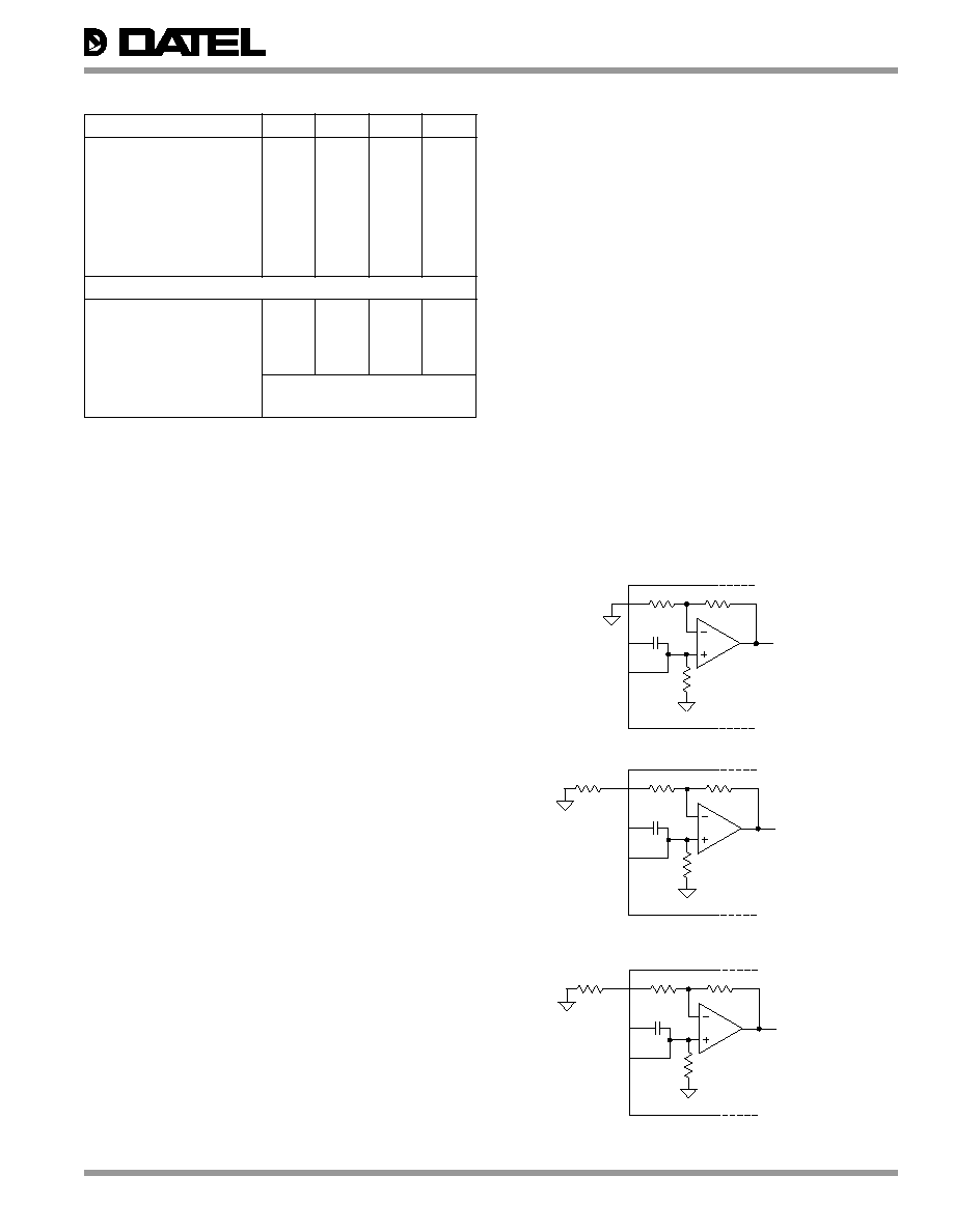
Direct Mode (AC Coupled)
This is the most common input configuration as it allows the
ADCDS-1403 to interface directly to the output of the CCD with
a minimum amount of analog "front-end" circuitry. This mode
of operation is used with full-scale video input signals from
0.350Vp-p to 2.8Vp-p.
Figure 2a. describes the typical configuration for applications
using a video input signal with a maximum amplitude of
0.350Vp-p. The coarse gain of the input amplifier is
determined from the following equation:
V
OUT
= 2.8Vp-p = V
IN
*(1+(523/75)), with all internal resistors
having a 1% tolerance. Additional fine gain adjustment can be
accomplished using the Fine Gain Adjust (pin 1 see Figure 5).
Figure 2b. describes the typical configuration for applications
using a video input signal with an amplitude greater than
0.350Vp-p and less than 2.8Vp-p. Using a single external
series resistor (see Figure 4.), the coarse gain of the ADCDS-
1403 can be set, with additional fine gain adjustments being
made using the Fine Gain Adjust function (pin 1 see Figure 5).
The coarse gain of the input amplifier can be determined from
the following equation:
V
OUT
= 2.8Vp-p = V
IN
*(1+(523/(75+Rext))), with all internal
resistors having a 1% tolerance.

ADCDS-1403
4
Æ
Æ
Inverting Mode
The inverting mode of operation can be used in applications
where the analog input to the ADCDS-1403 has a video input
signal whose amplitude is more positive than its associated
reference level.
The ADCDS-1403's correlated double
sampler (i.e. input amplifier's V
OUT
) requires that the video
signal's amplitude be more negative than its reference
level at all times (see timing diagram for details). Using the
ADCDS-1403 in the inverting mode allows the designer to
perform an additional signal inversion to correct for any
analog "front end" pre-processing that may have occurred
prior to the ADCDS-1403.
Figure 2e. describes the typical configuration for applications
using a video input signal with a maximum amplitude of
0.350Vp-p. Additional fine gain adjustments can be made
using the Fine Gain Adjust function (pin 1). The coarse gain
of this circuit can be determined from the following equation:
V
OUT
= 2.8Vp-p = ≠V
IN
*(523/75), with all internal resistors
having a 1% tolerance.
Figure 2f. describes the typical configuration used in
applications needing to invert video input signals whose
amplitude is greater than 0.350Vp-p. Using a single external
series resistor (see Figure 4.), the initial gain of the ADCDS-
1403 can be set, with additional fine gain adjustments being
made using the Fine Gain Adjust function (pin 1). The coarse
gain of this circuit can be determined from the following
equation:
V
OUT
= 2.8Vp-p = ≠V
IN
*(523/75+Rext), with all internal
resistors having a 1% tolerance.
Figure 4. Coarse Gain Adjustment Plot
Non-Inverting Mode
The non-inverting mode of the ADCDS-1403 allows the
designer to either attenuate or add non-inverting gain to the
video input signal. This configuration also allows bypassing
the ADCDS-1403's internal coupling capacitor, allowing the
user to provide an external capacitor of appropriate value.
Figure 2c. describes the typical configuration for applications
using video input signals with amplitudes greater than
0.350Vp-p and less than 2.8Vp-p (with common mode limit of
±2.5V DC). Using a single external series resistor (see
Figure 4.), the coarse gain of the ADCDS-1403 can be set
with additional fine gain adjustments being made using the
Fine Gain Adjust function (pin 1 see Figure 5). The coarse
gain of the circuit can be determined from the following
equation:
V
OUT
= 2.8Vp-p = V
IN
*(1+(523/(75+Rext))), with all internal
resistors having a 1% tolerance.
Figure 2d. describes the typical configuration for applications
using a video input signal whose amplitude is greater than
2.8Vp-p. Using a single external series resistor (Rext 1) in
conjunction with the internal 5K (1%) resistor to ground, an
attenuation of the input signal can be achieved. Additional fine
gain adjustments being made using the Fine Gain Adjust
function (pin 1). The coarse gain of this circuit can be
determined from the following equation:
V
OUT
= 2.8Vp-p = [V
IN
*(5000/(Rext1+5000))]*
[1+(523/(75+Rext2))], with all internal resistors having
a 1% tolerance.
Figure 2d.
Figure 2e.
4
3
5
75
9
523
9
NO CONNECT
V
OUT
= 2.8Vp-p
5k
9
0.01µF
Rext1
V
IN
Rext2
4
3
5
75
9
523
9
NO CONNECT
V
OUT
= 2.8Vp-p
5k
9
0.01µf
≠V
IN
4
3
5
75
9
523
9
NO CONNECT
V
OUT
= 2.8Vp-p
5k
9
0.01µf
≠V
IN
Rext
Figure 2f.
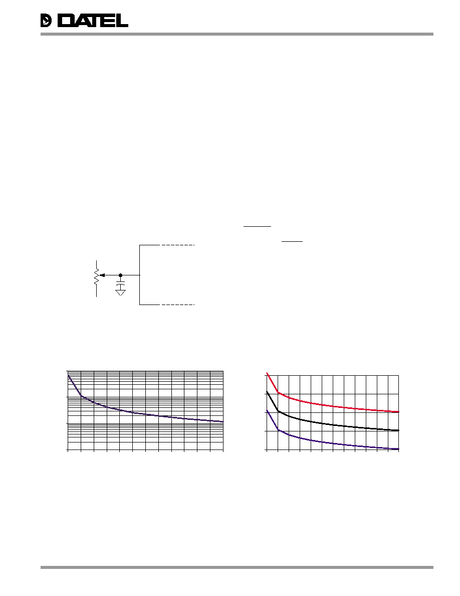
Figure 3. Offset Adjustment Circuit
Offset
Adjust
2
External
Series
Resistor
ADCDS-1403
+5V
≠5V
20K
9
C o a r s e G a i n A d j u s t m e n t P l o t
E x t e r n a l G a i n R e s i s t o r v s . F u l l S c a l e V i d e o I n p u t
1 0
1 0 0
1 0 0 0
1 0 0 0 0
0 . 2 5
0 . 5
0 . 7 5
1
1 . 2 5
1 . 5
1 . 7 5
2
2 . 2 5
2 . 5
2 . 7 5
3
F u l l S c a l e V i d e o S i g n a l ( V o l t s )
E
x
t
e
r
n
al
G
ai
n
R
esi
st
o
r
(
O
h
m
s
)
I n v e r t i n g M o d e
D i r e c t M o d e
& N o n - I n v e r t i n g
M o d e
ADCDS-1403
5
Æ
Æ
Figure 6. Offset Adjustment vs. External Series Resistor
Offset Adjustment vs. External Series Resistor
10
100
1000
10000
0
5k
10k
15k
20k
25k
30k
35k
40k
45k
50k
55k
60k
External Series Resistor (Ohm's)
±LS
B
'
s
of A
d
j
u
st
m
e
nt
Figure 5. Fine Gain Adjustment Circuit
ADCDS-1403
Fine
Gain
Adjust
1
+5V
≠5V
20K
9
External Series Resistor Value (Ohms)
0.01
0.1
1
10
100
0
5K
10K 15K 20K 25K 30K 35K 40K 45K 50K 55K 60K
Offset Adjustment Sensitivity
External Series Resistor vs. Output Variation (LSB's)
Out
put
Var
i
a
t
i
on (
L
SB'
s
)
Peak-Peak
variation at
potentiometer
1mV
10mV
100mV
Figure 7. Offset Adjustment Sensitivity
Offset Adjustment
Manual offset adjustment for the ADCDS-1403 can be
accomplished using the adjustment circuit shown in Figure
3. A software controlled D/A converter can be substituted for
the 20K
W
potentiometer. The offset adjustment feature
allows the user to adjust the Offset/Dark Current level of the
ADCDS-1403 until the output bits are 00 0000 0000 0000
and the LSB flickers between 0 and 1. Offset adjust should
be performed before gain adjust to avoid interaction. The
ADCDS-1403's offset adjustment is dependent on the value
of the external series resistor used in the offset adjust circuit
(Figure 3). The Offset Adjustment graph (Figure 6) illustrates
the typical relationship between the external series resistor
value and its offset adjustment capability utilizing ±5V
supplies.
Offset Adjustment Sensitivity
It should be noted that with increasing amounts of offset
adjustment (smaller values of external series resistors), the
ADCDS-1403 becomes more susceptible to power supply
noise or voltage variations seen at the wiper of the offset
potentiometer.
For Example:
External 50K
W
resistor:
1. 10mV of noise or voltage variation at the potentiometer
will produce 0.25LSB's of output variation.
2. 100mV of noise or voltage variation at the potentiometer
will produce 2.5LSB's of output variation.
The Offset Adjustment Sensitivity graph (Figure 7) illustrates
the offset adjustment sensitivity over a wide range of external
resistor and noise values. If a large offset voltage is required,
it is recommended that a very low noise external reference
be used in the offset adjust circuit in place of power supplies.
The ADCDS-1403's +2.4V reference output could be
configured to provide the reference voltage for this type of
application.
Fine Gain Adjustment
Fine gain adjustment (pin 1) is provided to compensate for
the tolerance of the external coarse gain resistor (Rext) and/
or the unavailability of exact coarse gain resistor (Rext)
values. Note, the fine gain adjustment will not change the
expected input amplifier's full scale V
OUT
(2.8Vp-p.) Instead,
the gain of the ADCDS-1403's internal A/D is adjusted
allowing the actual input amplifier's full scale V
OUT
to
produce an output code of all ones (11 1111 1111 1111).
Fine gain adjustment for the ADCDS-1403 is accomplished
using the adjustment circuit shown below (Figure 5). A
software controlled D/A converter can be substituted for the
20K
W
potentiometer. The fine gain adjust circuit ensures that
the video input signal (saturated signal) will be properly
scaled to obtain the desired Full Scale digital output of 11
1111 1111 1111, with the LSB flickering between 0 and 1. Fine
gain adjust should be performed following the offset adjust
ADCDS-1403
6
Æ
Æ
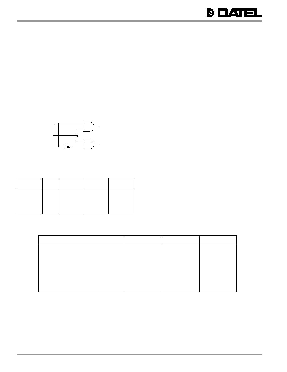
Table 1. Out-of-Range Conditions
Table 2. Output Coding
OUT
OVER
UNDER
INPUT
OF RANGE
MSB
RANGE
RANGE
SIGNAL
0
0
0
0
In Range
0
1
0
0
In Range
1
0
0
1
Underrrange
1
1
1
0
Overrange
Notes:
Input Amplifier V
OUT
= (Video Signal - Reference Level)
The video portion of the differential signal (input-amplifier's V
OUT
) must be more negative than its associated reference
level and V
OUT
should not exceed ±2.8V DC.
Video Signal-Reference Signal
> ≠2.80000
>Full Scale ≠1LSB
11 1111 1111 1111
1
≠2.80000
Full Scale ≠1LSB
11 1111 1111 1111
0
≠2.10000
3/4FS
11 0000 0000 0000
0
≠1.40000
1/2FS
10 0000 0000 0000
0
≠0.70000
1/4FS
01 0000 0000 0000
0
≠0.35000
1/8FS
00 1000 0000 0000
0
≠0.000171
1 LSB
00 0000 0000 0001
0
0
0
00 0000 0000 0000
0
Video Signal-Reference Signal
<0
<0
00 0000 0000 0000
1
INPUT AMPLIFIER V
OUT
,
¿
(VOLTS P-P)
SCALE
DIGITAL OUTPUT OUT-OF-RANGE
Output Coding
The ADCDS-1403's output coding is Straight Binary as
indicated in Table 2. The table shows the relationship between
the output data coding and the difference between the
reference signal voltage and its corresponding video signal
voltage. (These voltages are referred to the output of the
ADCDS-1403's input amplifier's V
OUT
).
Programmable Analog Bandwidth Function
When interfacing to CCD arrays with very high-speed "read-
out" rates, the ADCDS-1403's input stage must have sufficient
analog bandwidth to accurately reproduce the output signals
of the CCD array. The amount of analog bandwidth
determines how quickly and accurately the "Reference Hold"
and the "CDS output" signals will settle. If only a single analog
bandwidth was offered, the ADCDS-1403's bandwidth would
be set to acquire and digitize CCD output signals to 14-bit
accuracy, at maximum conversion rate of 3MHz (333ns see
Figure 11. for details). Applications not requiring the maximum
conversion rate would be forced to use the full analog
bandwidth at the possible expense of noise performance.
The ADCDS-1403 avoids this situation by offering a fully
programmable analog bandwidth function. The ADCDS-1403
allows the user to "bandwidth limit" the input stage in order to
realize the highest level of noise performance for the
application being considered. Table 3. describes how to
select the appropriate reference hold "aquisition time" and
CDS output "settling time" needed for a particular application.
Each of the selections listed in Table 3. have been optimized
to provide only enough analog bandwidth to acquire a full
scale input step, to 14-bit accuracy, in a single conversion.
Increasing the analog bandwidth (using a faster settling and
acquisition time) would only serve to potentially increase the
amount of noise at the ADCDS-1403's output. The ADCDS-
1403 uses a two bit digital word to select four different analog
bandwidths for the ADCDS-1403's input stage (See Table 3.
for details).
MSB
OUT-OF-RANGE
"OVERRANGE"
"UNDERRANGE"
Figure 8. Overrange/ Underrange Circuit
to avoid interaction. The fine gain adjust provides ±256 codes
of adjust when ±5V supplies are used for the Fine Gain Adjust
Circuit.
Out-of-Range Indicator
The ADCDS-1403 provides a digital Out-of-Range output
signal (pin 24) for situations when the video input signal
(saturated signal) is beyond the input range of the internal A/D
converter. The digital output bits and the Out-of-Range signal
correspond to a particular sampled video input voltage, with
both of these signals having a common pipeline delay.
Using the circuit described in Figure 8., both overrange and
underrange conditions can be detected (see Table 1). When
combined with a D/A converter, digital detection and orrection
can be performed for both the gain and offset errors.

ADCDS-1403
7
Æ
Æ
Table 3. Programmable Analog Bandwidth
REFERENCE HOLD
CDS OUTPUT
A0
A1
ADCDS-1403 MAXIMUM
"AQUISITION TIME"
"SETTLING TIME"
(Pin 30)
(Pin 31)
CONVERSION RATE
≠3dB BW
100ns
120ns
0
0
3MHz
10.5MHz
200ns
250ns
1
0
2MHz
6.6MHz
450ns
500ns
0
1
1MHz
3.7MHz
600ns
1000ns
1
1
0.5MHz
2.5MHz
Note: See Figure 11. for timing details
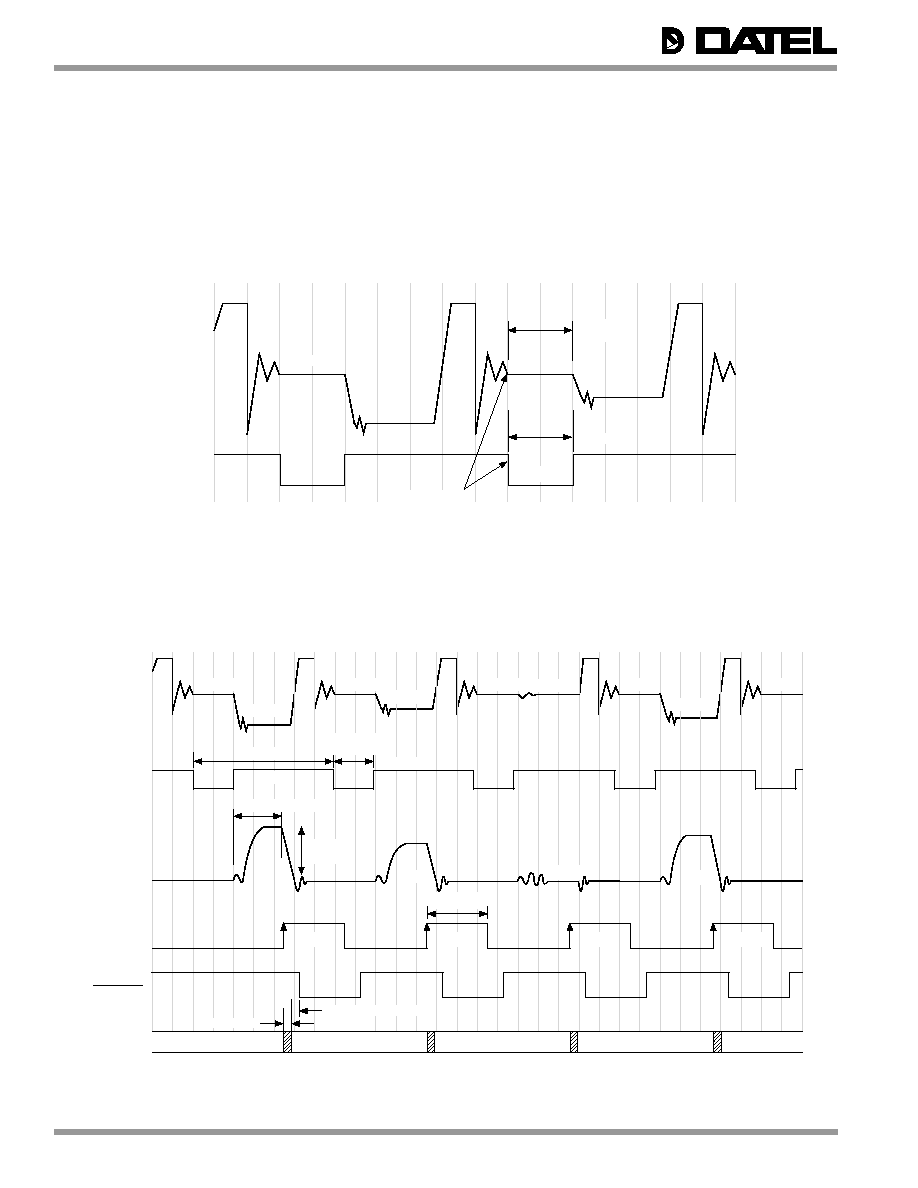
Timing
The ADCDS-1403 requires two independently operated
signals to accurately digitize the analog output signal from the
CCD array.
∑
Reference Hold (pin 26)
∑
Start Convert (pin 25)
The "Reference Hold" signal controls the operation of an
internal sample-hold circuit. A logic "1" places the sample-
hold into the hold mode, capturing the value of the CCD's
Figure 9. ADCDS-1403 Connection Diagram
reference signal. The Reference Hold Signal allows the user
to control the exact moment when the sample-hold is placed
into the "hold" mode. For optimal performance the sample-
hold should be placed into the "hold" mode once the
reference signal has fully settled from all switching
transients to the desired accuracy (user defined).
Once the reference signal has been "held" and the video
portion of the CCD's analog output signal appears at the
ADCDS-1403's input, the ADCDS-1403's correlated double
sampler produces a "CDS Output" signal (see Figure 11.)
+
+
+
+ 1 2 V
+ 5 V D
5 V A
4 . 7 µ F
0 . 1 µ F
3 9 3 6
3 8
1
2 0 K
9
+ 5 V
5 V
5
4
3
2 3
2 2
2 1
2 0
1 9
1 8
1 7
1 6
1 5
1 4
1 3
1 2
1 1
1 0
B I T 1 ( M S B )
B I T 2
B I T 3
B I T 4
B I T 5
B I T 6
B I T 7
B I T 8
B I T 9
B I T 1 0
B I T 1 1
B I T 1 2
B I T 1 3
B I T 1 4 ( L S B )
6
2 4
2 7
+ 2 . 4 V R E F E R E N C E O U T
O U T - O F - R A N G E
D A T A V A L I D
A D C D S - 1 4 0 3
4 . 7 µ F
0 . 1 µ F
4 . 7 µ F
0 . 1 µ F
A N A L O G G R O U N D
N O N - I N V E R T I N G I N P U T
I N V E R T I N G I N P U T
D I R E C T I N P U T
+ 5 V A
3 6
7 , 3 5 , 3 7
+
4 . 7 µ F
0 . 1 µ F
2 6
2 5
R E F . H O L D
S T A R T C O N V E R T
2
2 0 K
9
+ 5 V
5 V
O F F S E T A D J U S T
F I N E G A I N A D J U S T
E x t e r n a l S e r i e s
R e s i s t o r
3 2 , 3 3 D I G I T A L G R O U N D
3 0
3 1
A 1
A
0 . 1 µ F
0 . 1 µ F
ADCDS-1403
8
Æ
Æ
Figure 11. ADCDS-1403 Timing Diagram
Figure 10. Reference Hold Timing
which is the difference between the "held" reference level
and its associated video level. When the "CDS Output" signal
has settled to the desired accuracy (user defined), the A/D
conversion process can be initiated with the rising edge of a
single start convert (Pin 25) signal.
Once the A/D conversion has been initiated, Reference Hold
(Pin 26) can be placed back into the "Acquisition" mode in
order to begin aquiring the next reference level. For optimal
performance the ADCDS-1403's internal sample-hold should
be placed back into the "Aquisition" mode (Reference Hold to
logic "0") during the CCD's "Reference Quiet Time"
("Reference Quiet Time" is defined as the period when the
CCD's reference signal has settled from all switching
transients to the desired accuracy (see Figure 10.)). Placing
the sample-hold back into the "aquisition" mode during the
"Reference Quiet Time" prevents the ADCDS-1403's internal
amplifiers from unecessarily tracking (reproducing) the large
switching transients that occur during the CCD's reset to
reference transition.
C C D
O U T P U T
R E F E R E N C E
H O L D
N o t e : F o r o p t i m a l p e r f o r m a n c e ( F a s t e s t A c q u i s i t i o n T i m e ) , t h e A D C D S - 1 4 0 3 s h o u l d b e p l a c e d i n t o t h e A c q u i s i t i o n m o d e ( R e f e r e n c e H o l d t o l o g i c " 0 " )
d u r i n g t h e C C D o u t p u t ' s R e f e r e n c e " Q u i e t T i m e " . R e f e r e n c e " Q u i e t T i m e " i s d e f i n e d a s t h e p e r i o d w h e n t h e r e f e r e n c e s i g n a l ' s s w i t c h i n g t r a n s i e n t s
h a v e s e t t l e d t o a n a c c e p t a b l e ( u s e r d e f i n e d ) a c c u r a c y .
H O L D
R e s e t
V i d e o
R e f e r e n c e
R e f e r e n c e
" Q u i e t T i m e "
1 0 0 N S M I N .
A c q u i s i t i o n T i m e
A c q u i s i t i o n m o d e d u r i n g
R e f e r e n c e " Q u i e t T i m e "
R e s e t N
R e s e t N + 1
R e s e t N + 2
R e s e t N + 3
R e s e t N + 4
N o t e : A s d e s c r i b e d i n F i g u r e 1 0 , t h e 6 0 n s m i n . i s d e p e n d a n t o n t h e q u a l i t y o f t h e C C D ' s R e f e r e n c e w h e n t h e A D C D S - 1 4 0 3 i s s w i t c h e d b a c k i n t o t h e t r a c k m o d e
C C D
O U T P U T
S T A R T
C O N V E R T
R E F E R E N C E
H O L D I N
C D S
O U T P U T
D A T A
O U T P U T
1 0 0 n s m i n .
1 3 3 n s m i n
1 2 0 n s m i n s e t t l i n g l i n e
F u l l S c a l e
S t e p
1 5 0 n s m i n
D A T A N - 4 V A L I D
D A T A N - 3 V A L I D
D A T A N - 2 V A L I D
D A T A N - 1 V A L I D
D A T A N V A L I D
2 0 n s m i n
N
R e f N
V i d e o N
R e f . N + 1
V i d e o N + 1
1 0 0 n s m i n .
3 3 3 n s m i n .
1 2 0 n s m i n . s e t t l i n g t i m e
1 5 0 n s t y p .
2 0 n s m a x
R e f . N
V i d e o N
V i d e o N + 1
R e f . N + 2
V i d e o N + 1
V i d e o N + 2
R e f . N + 3
V i d e o N + 1
V i d e o N + 3
R e f . N + 4
N + 2
N + 3
N
N + 1
N + 2
N + 3
H o l d
A c q u i s i t i o n
T i m e
N + 1
I n v a l i d d a t a
3 0 n s m i n . , 5 0 n s m a x .
D A T A V A L I D
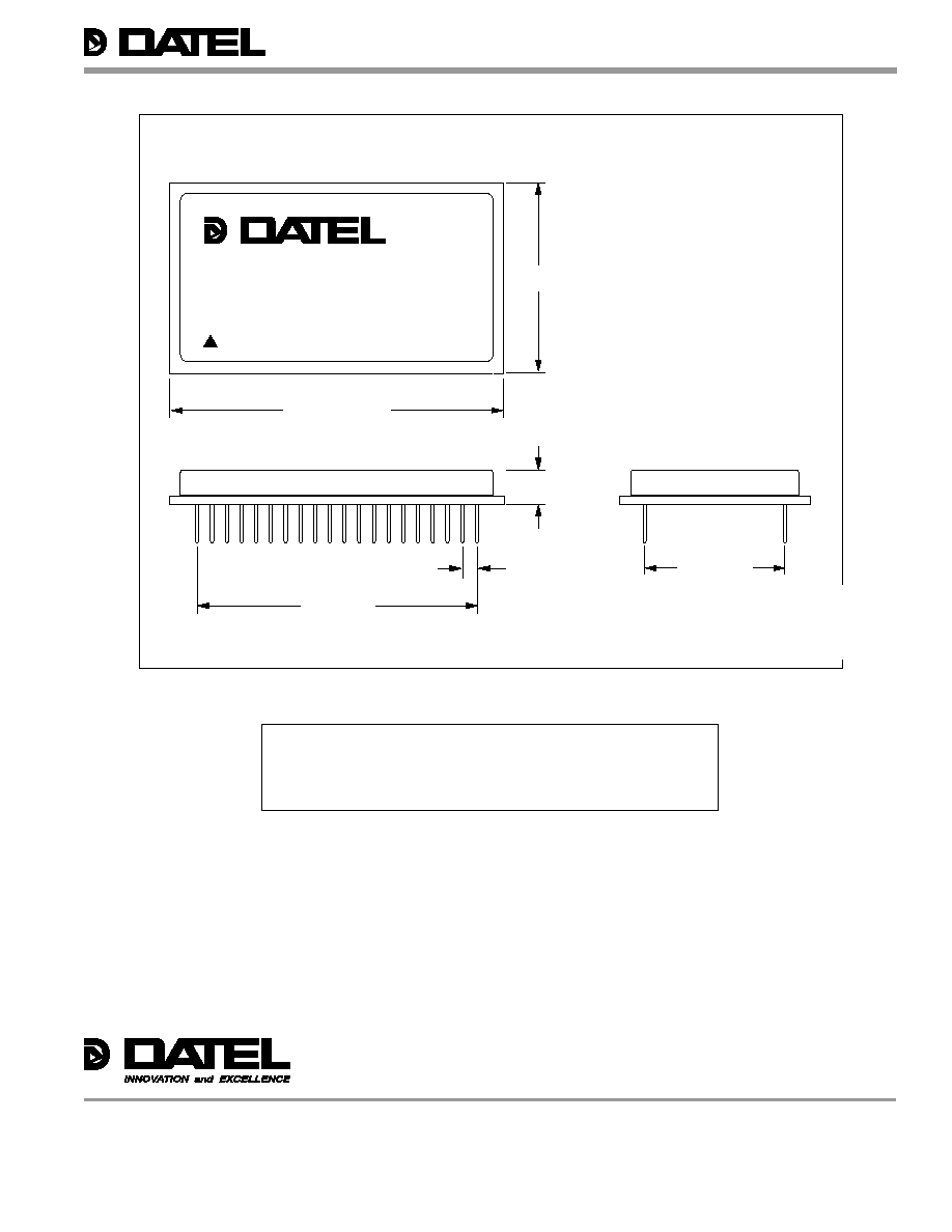
MECHANICAL DIMENSIONS INCHES (mm)
ORDERING INFORMATION
OPERATING
40-PIN
MODEL
TEMPERATURE RANGE
PACKAGE
ADCDS-1403
0 to 70∞C
TDIP
ADCDS-1403EX
≠55 to 125∞C
TDIP
DATEL, Inc. 11 Cabot Boulevard, Mansfield, MA 02048-1151
Tel: (508) 339-3000 (800) 233-2765 Fax: (508) 339-6356
Internet: www.datel.com Email: sales@datel.com
DATEL makes no representation that the use of its products in the circuits described herein, or the use of other technical information contained herein, will not infringe upon existing or future patent rights. The descriptions contained herein
do not imply the granting of licenses to make, use, or sell equipment constructed in accordance therewith. Specifications are subject to change without notice. The DATEL logo is a registered DATEL, Inc. trademark.
DATEL (UK) LTD. Tadley, England Tel: (01256)-880444
DATEL S.A.R.L. Montigny Le Bretonneux, France Tel: 01-34-60-01-01
DATEL GmbH Munchen, Germany Tel: 89-544334-0
DATEL KK Tokyo, Japan Tel: 3-3779-1031, Osaka Tel: 6-354-2025
DS-332A
05/2000
Æ
Æ
ISO 9001
ISO 9001
R E G I
S T E R E D
ADCDS-1403
Æ
Æ
0 . 1 0 0 T Y P .
( 2 . 5 4 0 )
2 . 2 4 T Y P .
( 5 6 . 9 0 )
0 . 9 0 0 ± 0 . 0 1 0
( 2 2 . 8 6 )
1 . 9 0 0 ± 0 . 0 0 8
( 4 8 . 2 6 0 )
0 . 2 3 T Y P .
( 5 . 8 4 )
1 . 2 7 T Y P .
( 3 2 . 2 5 )
Æ
Æ
A D C D S - 1 4 0 3
1 4 - B I T , 3 M H z
I M A G I N G S I G N A L P R O C E S S O R
M a d e i n U S A