HL02RrevD,10/97
Page 1
oscillator in the input stage with low-drop regula-
tors on the outputs reducing the output noise and
maintaining good efficiency.
The use of surface mount construction and auto-
mated manufacturing processes increase consistency
and reliability while reducing overall cost.
T
YPICAL PERFORMANCE CURVES
Specifications typical at T
A
= +25∞C, nominal input voltage, rated output current unless otherwise specified.
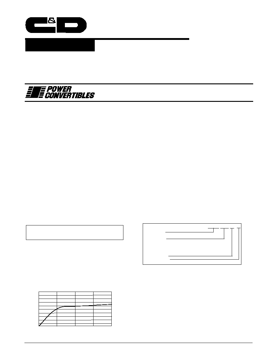
EFFICIENCY vs LOAD
100%
50%
0%
50%
75%
100%
0%
25%
ABSOLUTE MAXIMUM RATINGS
Internal Power Dissipation.......................................................1.5W
Short Circuit Duration....................................................Continuous
Lead Temperature (soldering, 10 seconds max)................+300∞C
*
Note: Refer to Reflow Profile for SMD Models.
*
ORDERING INFORMATION
Device Family
HL Indicates DC/DC Converter
Model Number
Where:
xx = Input Voltage
y = Number or Outputs (Single "S", Dual "D")
zz = Output Voltage
Package Option
Screening Option
DIP Package only
q
q
q
q
q
SURFACE MOUNT CONSTRUCTION
q
q
q
q
q
TEMPERATURE RANGE: -25∞C TO +70∞C
FEATURES
q
q
q
q
q
LOW COST
q
q
q
q
q
INTERNAL FILTERING
q
q
q
q
q
LOW OUTPUT NOISE
q
q
q
q
q
SHORT CIRCUIT PROTECTION
DESCRIPTION
The HL02R Series offers an extensive selection of
input and output voltage combinations to choose
from. These minature, regulated DC/DC converters
come in a 24 pin DIP and SMD packages. This small
size is possible through the use of surface mount
manufacturing technologies.
The HL02R Series utilizes a 110KHz push-pull
HL02R xxyzz Y/Z /H
TECHNOLOGIES
Product Data Sheet
2 W
ATTS
R
EGULATED
DC/DC C
ONVERTER
HL02R
TM
3400 E Britannia Dr, Ste 122
l Tucson, Arizona 85706 l Phone: 520.628.8292 l Fax: 520.770.9369 l Internet: http://www.pcc1.com

HL02RrevD,10/97
Page 2
PARAMETER
CONDITIONS
MIN
TYP
MAX
UNITS
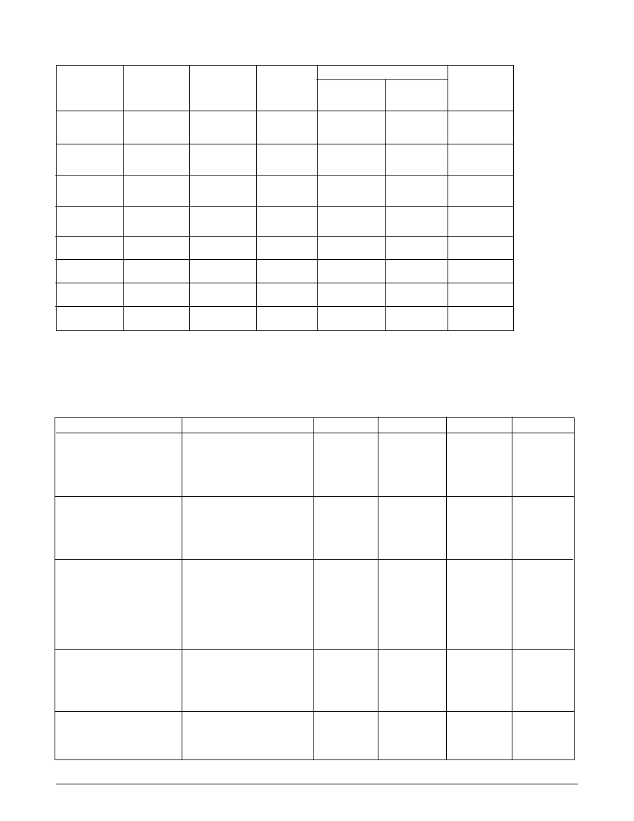
INPUT
Voltage Range
4.75
5
5.25
VDC
11.4 12 12.6
VDC
14.25
15
15.75
VDC
22.8
24
25.2
VDC
Reflected Ripple Current
30
100
mAp-p
ISOLATION
Rated Voltage
500
VDC
Test Voltage
60 Hz, 10 Seconds
500
Vpk
Resistance
1
G
Capacitance
25
pF
Leakage Current
V
ISO
= 240VAC, 60Hz
2
µArms
OUTPUT
Rated Power
2
W
Voltage Setpoint Accuracy
±0.5
±5
%
Temperature Coefficent
±0.02
%/∞C
Ripple & Noise
BW = DC to 10MHz
25
100
mVp-p
BW =10Hz to 2MHz
10
mVrms
5V Output - Singles Only
250
350
mVp-p
Line Regulation
High Line to Low Line ±0.5
±1.0
%
Load Regulation
Rated Load to No Load ±0.1
±0.5
%
GENERAL
Switching Frequency
110
kHz
Package Weight
12
g
MTTF per MIL-HDBK-217, Rev. F
Circuit Stress Method
Ground Benign
T
A
= +25∞C
1100
kHr
T
A
= +70∞C
20
kHr
TEMPERATURE
Specification
-25
+70
∞C
Operation
-40
+85
∞C
Storage
-40
+110
∞C
NOMINAL
RATED
RATED
INPUT CURRENT
INPUT
OUTPUT
OUTPUT
VOLTAGE
VOLTAGE
CURRENT
NO LOAD
RATED LOAD
EFFICIENCY
MODEL
(VDC)
(VDC)
(mA) (mA) (mA)(%)
HL02R05S05
5
5
400
70
640
62
HL02R05S12
5
12
166
70
580
69
HL02R05S15
5
15
134
70
580
69
HL02R12S05
12
5
400
40
280
60
HL02R12S12
12
12
166
40
250
67
HL02R12S15
12
15
134
40
250
67
HL02R15S05
15
5
400
30
230
58
HL02R15S12
15
12
166
30
200
67
HL02R15S15
15
15
134
30
200
67
HL02R24S05
24
5
400
15
135
62
HL02R24S12
24
12
166
15
120
67
HL02R24S15
24
15
134
15
120
67
HL02R05D12
5
±12
±83
70
640
62
HL02R05D15
5
±15
±67
70
640
62
HL02R12D12
12
±12
±83
40
270
62
HL02R12D15
12
±15
±67
40
270
62
HL02R15D12
15
±12
±83
30
220
61
HL02R15D15
15
±15
±67
30
220
61
HL02R24D12
24
±12
±83
15
135
62
HL02R24D15
24
±15
±67
15
135
62
Note: Other input to output voltages may be available. Please consult factory.
Specifications typical at T
A
= +25∞C, nominal input voltage, rated output current unless otherwise specified.
COMMON SPECIFICATIONS
ELECTRICAL SPECIFICATIONS
Specifications typical at T
A
= +25∞C, nominal input voltage, rated output current unless otherwise specified.

HL02RrevD,10/97
Page 3
0.100±0.010"
(2.54±0.25)
0.020±0.002"
(0.51±0.05)
0.015±0.005"
(0.38±0.13)
0.375±0.005"
(9.52±0.13)
1.285±0.010"
(32.64±0.25)
24 23 22
15 14 13
12
11
10
3
2
1
0.014±0.002"
(0.36±0.05)
.015±.010"
(.38±.25)
0.525±0.010"
(13.34±0.25)
0.695±0.015"
(17.65±0.38)
Package/Pinout "Y" and "Z"
0∞-
15
∞
0.125+0.030"
-0.000"
(3.18+0.76)
( -0.00)
0.600"
(15.24)
0.100±0.010"
(2.54±0.25)
0.020±0.002"
(0.51±0.05)
0.015±0.005"
(0.38±0.13)
0.375±0.005"
(9.52±0.13)
1.285±0.010"
(32.64±0.25)
24 23 22
15 14 13
12
11
10
3
2
1
0.525±0.010"
(13.34±0.25)
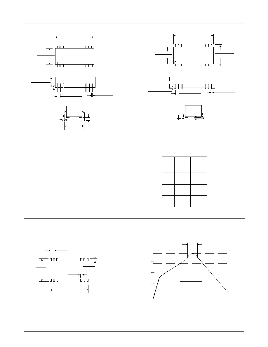
SIDE VIEWS
TOP VIEWS
END VIEWS
SMD PACKAGE
DIP PACKAGE
HL02RxxyzzY
HL02RxxyzzZ
PIN CONNECTIONS
RECOMMENDED LAND PATTERN
24 23 22
15 14 13
12
11
10
3
2
1
0.730"
(18.54)
1.150"
(29.21)
0.100"
(2.54)
0.080"
(2.03)
0.040"
(1.02)
50
100
150
200
250
TEMPERA
TURE (∞C)
TIME (seconds)
235 ∞C MAX
220
190
30 sec MAX
(>220∞C)
90 sec MAX
(>190∞C)
RECOMMENDED REFLOW PROFILE
NC = No Internal Connection.
NU = Do Not Use.
Duplicate pin functions are internally connected.
All dimensions are in inches (millimeters).
GRID: 0.100 inches (2.54 millimeters)
Typically Marked with: specific model ordered, date
code, job code and Logo.
MECHANICAL
PIN# SINGLES DUALS
1
+VIN
+VIN
2
NU
-VOUT
3
NU
Common
10
-VOUT
Common
11
+VOUT
+VOUT
12
-VIN
-VIN
13
-VIN
-VIN
14
+VOUT
+VOUT
15
-VOUT
Common
22
NU
Common
23
NU
-VOUT
24
+VIN
+VIN
