Page 1
HPR2XX REV D 4/99
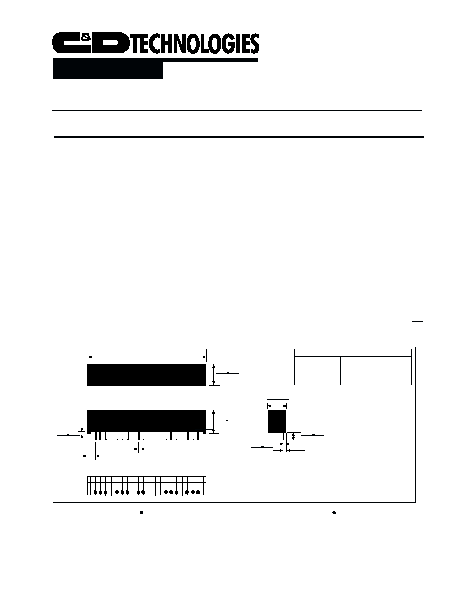
MECHANICAL
RIGHT
SIDE
VIEW
FRONT
VIEW
BOTTOM
VIEW
TOP
VIEW
1 2 3 5 6 7 9 10 14 15 16 18 19 20
All dimensions are in inches (millimeters).
GRID: 0.100 inches (2.54 millimeters)
PIN PLACEMENT TOLERANCE: ± 0.015"
Marked with: specific model ordered, date code, and job code.
0.155+.015
(3.94)
0.030+.010
(0.76)
2.210+.010
(56.13)
0.340+.010
(8.64)
0.400+.010
(10.16)
0.010+.002
(0.25)
0.140+.020
(0.25)
FEATURES
!
!
!
!
!
Four Channels Of Isolated Power
!
!
!
!
!
High Output Power Density: > 9. 4 Watts/Inch
3
!
!
!
!
!
Extended Temperature Range:
-25∞C To +85∞C
!
!
!
!
!
High Efficiency: To 84%
!
!
!
!
!
Low Cost
Product Data Sheet
!
!
!
!
!
High Isolation Voltage: 750V Continuous
Input-to-Output and Channel-to-Channel
!
!
!
!
!
Single In-line Package (SIP)
!
!
!
!
!
Internal Input and Output Filtering
!
!
!
!
!
Non-Conductive Case
The HPR2XX Series is designed for multiple channel applications
that require small size and could benefit from a complete one-
package solution. The HPR2XX Series offers four isolated
channels of output power in a footprint less than the size of many
singular devices. This unregulated series of DC/DC converters
provides three watts of total output power. Each isolated channel
can supply up to 750mW.
The HPR2XX Series uses advanced circuit design and packaging
technology to realize superior reliability and performance. With
only one switching converter on the board, the HPR2XX
eliminates the possibility of separate converters creating beat
frequencies, or "aliasing" in multiple channel applications.
The high efficiency of the HPR2XX Series means less internal
power dissipation than comparable solutions. With reduced heat
to dissipate, the HPR2XX Series can operate at higher
temperatures with no degradation in reliablility. In addition, the
high efficiency of the HPR2XX Series provides greater than 9
watts/inch
3
output power density.
The HPR2XX Series offers the user low cost without sacrificing
reliability. The use of surface mounted devices and manufacturing
technologies make it possible to offer premium performance and
low cost.
3.0 W
ATT
M
INIATURE
SIP DC/DC C
ONVERTER
HPR2XX
Internet: http://www.cdpowerelectronics.com
Power Electronics Division, United States
3400 E Britannia Drive, Tucson, Arizona 85706
Phone: 800.547.2537 Fax: 520.770.9369
Power Electronics Division, Europe
C&D Technologies (Power Electronics) Ltd.
132 Shannon Industrial Estate, Shannon, Co. Clare, Ireland
Tel: +353.61.474.133 Fax:+353.61.474.141
0.020+.002
(0.51)
0.340+.010
(8.64)
PIN CONNECTIONS
1. -VOUT1 5.-VOUT2
9. +VIN
14. -VOUT3
18. -VOUT4
2. COM 1 6. COM2
10.-VIN 15. COM3
19. COM 4
3 +VOUT1 7.+VOUT2
16. +VOUT3 20. +VOUT4
0.050+.015
(1.27)
Page 2
HPR2XX REVD 4/99
Device Family
HPR Indicates DC/DC Converter
Model Number
Selected From Table Above
Screening Option
ORDERING INFORMATION
ELECTRICAL SPECIFICATIONS
Specifications typical at T
A
= +25∞C, nominal input voltage, rated output current unless otherwise specified.
HPR 2XX /H
NOMINAL
RATED
RATED
INPUT CURRENT
REFLECTED
INPUT
OUTPUT
OUTPUT
RIPPLE
VOLTAGE VOLTAGE CURRENT
NO LOAD
RATED LOAD CURRENT
EFFICIENCY
MODEL
(VDC)
(VDC)
(mA)
(mA) (mA)
(mAp-p)
(%)
HPR203
5
±5.2
±73
70
820
35
74
HPR204
5
±12
±30
75
750
35
80
HPR205
5
±15
±25
75
750
35
80
HPR210
12
±12
±30
30
305
15
82
HPR211
12
±15
±25
30
300
15
84
HPR216
15
±12
±30
20
240
15
83
HPR217
15
±15
±25
20
240
20
84
HPR221
24
±5.0
±75
20
170
20
74
HPR223
24
±15
±25
20
155
20
81
Note: Other input to output voltage options may be available. Please consult factory.
COMMON SPECIFICATIONS
PARAMETER
CONDITIONS
MIN
TYP
MAX
UNITS
INPUT
Voltage Range
4.5
5
5.5
VDC
10.8
12
13.2
VDC
13.5
15
16.5
VDC
21.6
24
26.4
VDC
Voltage Rise Time
1
V/µsec
In Rush Current
At Startup
Amps
ISOLATION
Rated Voltage
Input to Output, Channel to Channel
750
VDC
Test Voltage
60 Hz, 10 seconds
750
Vpk
Resistance
10
G
Capacitance
30
pF
Leakage Current
V
ISO
= 240VAC, 60Hz
4
µArms
OUTPUT
Total Rated Power
3
W
Rated Power Each Channel
750
mW
Voltage Setpoint Accuracy
Rated Load, Nominal V
IN
±5
%
Ripple & Noise
BW = DC to 10MHz
40
mVp-p
BW =10Hz to 2MHz
7
mVrms
Voltage
I
L
=1mA, V
OUT
= 5V
8
VDC
I
L
=1mA, V
OUT
= 12V
17
VDC
I
L
=1mA, V
OUT
= 15V
20
VDC
Temperature Coefficent
.05
%/Deg C
REGULATION
Line Regulation
High Line to Low Line
1
%/%V
IN
Load Regulation (5V out only)
Rated Load to 1mA Load
10
%
Load Regulation (All other Models)
Rated Load to 1mA Load
3
%
GENERAL
Switching Frequency
300
kHz
Package Weight
7
g
Frequency Change
Rated Load to 1mA Load
5
%
High Line to Low Line
20
%
MTTF per MIL-HDBK-217, Rev. E
Circuit Stress Method
Ground Benign
T
A
= +25∞C
1.8
MHr
Fixed Ground
T
A
= +35∞C
450
kHr
Naval Sheltered
T
A
= +35∞C
270
kHr
Airborne Uninhabited Fighter
T
A
= +35∞C
45
kHr
TEMPERATURE
Specification
-25
+25
+85
∞C
Operation
-40
+100
∞C
Storage
-40
+110
∞C
ABSOLUTE MAXIMUM RATINGS
Internal Power Dissipation............................................................................1.2W
Short Circuit Protection.......................................................................< 1 second
Lead Temperature (soldering, 10 seconds max)......................................+300∞C
Specifications typical at T
A
= +25∞C, nominal input voltage, rated output current unless otherwise specified.
Page 3
HPR2XX REV D 4/99
The information provided herein is believed to be reliable; however, C&D TECHNOLOGIES assumes no responsibility for inaccuracies or omissions. C&D TECHNOLOGIES assumes no responsibility
for the use of this information, and all use of such information shall be entirely at the user's own risk. Prices and specifications are subject to change without notice. No patent rights or licenses to any
of the circuits described herein are implied or granted to any third party. C&D TECHNOLOGIES does not authorize or warrant any C&D TECHNOLOGIES product for use in life support devices/systems
or in aircraft control applications.
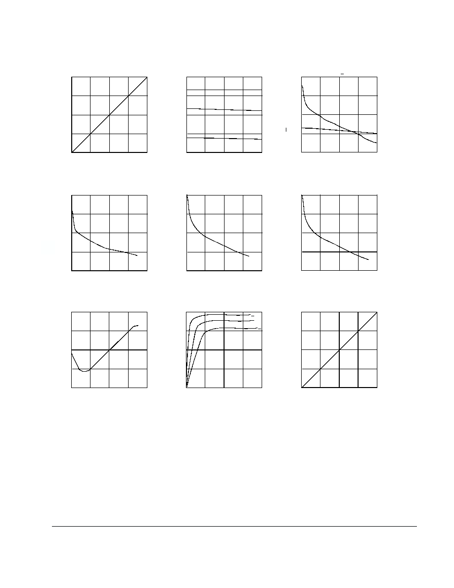
Frequency (kHZ)
Frequency (kHZ)
400
375
350
325
300
420
390
360
330
300
31.0
30.5
30.0
29.5
29.0
6.6
6.2
5.8
5.4
5.0
14.0
13.4
12.8
12.2
11.6
16.00
15.75
15.50
15.25
15.00
50.0
37.5
25.0
12.5
0
90.0
67.5
45.0
22.5
0
12
6
0
-6
-12
+V
OUT
(VDC)
V
OUT
(VDC)
V
OUT
(VDC)
V
OUT
(VDC)
Reflected Ripple Current (mA p-p)
Efficiency (Pout/Pin)
Change from Nom Vout (%)
-10 -5 0 5 10
0 .85 1.7 2.6 3.5
0 0.8 1.7 2.6 3.4
-0 6.25 12.50 18.75 25
0 8 16 24 32
0 20 40 60 80
0 6 12 18 26
0 .75 1.5 2.25 3.0
4.5 4.75 5.0 5.25 5.5
Vin (VDC)
Pout (Watts)
Input Channel 1 (mA)
Iout (mA sum of all Outputs)
Iout (mA sum of all Outputs)
Iout (mA sum of all Outputs)
Pout (Watts)
Pout (Watts)
Pout (Watts)
REFLECTED RIPPLE CURRENT vs. Pout
EFFICIENCY vs OUTPUT POWER
LINE REGULATION
LOAD REGULATION
(5 Vout Models)
LOAD REGULATION
(12 Vout Models)
LOAD REGULATION
(15 Vout Models)
FREQUENCY vx VIN
FREQUENCY vs Pout
CROSS REGULATION HPR205
Channels 2-4: +25mA Load
High
Line
Nominal
Line
Low
Line
Channel 2-4
Channel 1
+15Vout
+12Vout
+5Vout
TYPICAL PERFORMANCE CURVES
Specifications typical at T
A
= +25∞C, nominal input voltage, rated output current unless otherwise specified.