 | –≠–ª–µ–∫—Ç—Ä–æ–Ω–Ω—ã–π –∫–æ–º–ø–æ–Ω–µ–Ω—Ç: HPR7XX | –°–∫–∞—á–∞—Ç—å:  PDF PDF  ZIP ZIP |
Page 1
HPR7XX REV B 6/98
3400 E. Britannia Drive ∑ Tucson, Arizona 85706 ∑ Phone: 520.295.4100 ∑ Fax: 520.770.9369 ∑ Internet: http://www.cdpowerelectronics.com
Product Data Sheet
5 W
ATT
U
NREGULATED
SIP DC/DC C
ONVERTER
HPR7XX
DESCRIPTION
The HPR7XX Series provides high power densities where space
is critical. The small SIP package measures only 2.2" x .3" x .4"
(56 x 9 x 10 mm). Designed for high density boards, the package
is non-conductive, which presents advantages over painted
metal enclosures.
The series includes many different voltage models (other input
and output voltages are available upon request), all set in a low
thermal resistance molding compound, called Iso-ThermoFlex
TM
,
which provides excellent heat dissipation of internal compo-
nents. The use of surface mount devices and manufacturing
processes, combined with the encapsulation process, assure the
user that the product is more environmentally rugged than any
other DC/DC converter of its type.
Operation down to no load will not impact the reliability of the
series, although this product has a 10mA minimum load for
specification purposes. It is recommended that all pins be used
for current carrying capacity even though duplicate pin-outs are
internally connected.
The HPR7XX has 500VDC isolation barrier between input and
output, offering the designer maximum flexibility in grounding
options and polarity configurations. The outstanding MTTF,
superior reliability, and low cost make it an excellent choice for
any high power- density applications.
FEATURES
q
q
q
q
q
EFFICIENCY >80%
q
q
q
q
q
SIP PACKAGE
q
q
q
q
q
HIGH POWER DENSITY: > 16 WATTS/INCH
3
q
q
q
q
q
LOW COST
q
q
q
q
q
SINGLE AND DUAL OUTPUTS
q
q
q
q
q
INTERNAL INPUT AND OUTPUT
FILTERING
q
q
q
q
q
SIX-SIDED SHIELDING
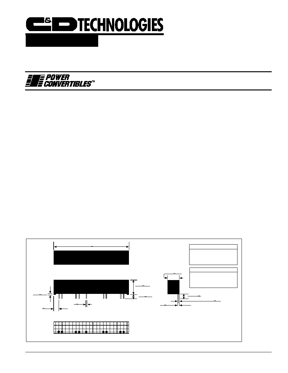
MECHANICAL
15. COM
19. COM
20. -VOUT
15. +VOUT
19. -VOUT
20. -VOUT
7. -VIN
9. -VIN
14. +VOUT
1. +VIN
2. +VIN
6. -VIN
All dimensions are in inches (millimeters)
GRID: 0.100 inches (2.54 millimeters)
PIN PLACEMENT TOLERANCE: ±0.015"
1. +VIN
2. +VIN
6. -VIN
7. -VIN
9. -VIN
14. +VOUT
PIN CONNECTIONS: Duals
PIN CONNECTIONS: Singles
TOP
VIEW
FRONT
VIEW
BOTTOM
VIEW
RIGHT SIDE
VIEW
2.210 + 0-.10
(56.13)
0.020 + .002
(0.51)
0.155 + -.15
(3.94)
0.030 + -.010
(0.76)
0.400 + .010
(10.16)
0.140 + .020
(3.56)
0.340 + .010
(8.64)
0.010 + .002
(0.25)
0.050 + .015
(1.27)
0.140 + .020
(3.56)
C L
1 2 6 7 9 14 15 19 20
Page 2
HPR7XX REV B 6/98
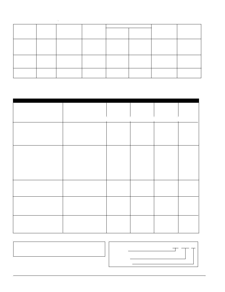
NOMINAL
RATED
RATED
INPUT CURRENT
REFLECTED
INPUT
OUTPUT
OUTPUT
NO LOAD
RATED LOAD
RIPPLE
EFFICIENCY
VOLTAGE
VOLTAGE
CURRENT
CURRENT
MODEL
(VDC) (VDC)
(mA)
(mA) (mA)
(mAp-p)
(%)
HPR700
5
5
1000
70
1250
15
80
HPR703
5
± 5
±500
70
1250
15
80
HPR704
5
±12
±208
70
1190
15
84
HPR705
5
±15
±167
70
1190
15
84
HPR706
12
5
1000
25
490
15
80
HPR710
12
±12
±208
25
490
15
85
HPR711
12
±15
±167
25
490
15
85
HPR712
15
5
1000
20
407
15
82
HPR717
15
±15
±167
20
392
15
85
Note: Other input to output voltage options may be available. Please consult factory.
ELECTRICAL CHARACTERISTICS
Specifications typical at T
A
= +25∞C, nominal input voltage, rated output current unless otherwise specified.
ORDERING INFORMATION
HPR 7XX /H
Device Family
HPR indicates DC/DC converter
Model Number
Screening Option
COMMON SPECIFICATIONS
Specifications typical at T
A
= +25∞C, nominal input voltage, rated output current unless otherwise specified.
PARAMETER
CONDITIONS
MIN
TYP
MAX
UNITS
INPUT
Voltage Range
4.75
5
5.25
V
DC
11.4
12
12.6
V
DC
14.2
15
15.8
V
DC
Voltage Rise Time
See Application Note: "Capacitive Loading Effects on Start-Up of DC/DC Converters"
ISOLATION
Rated Voltage
500
V
DC
Test Voltage
60 Hz, 10 seconds
500
Vpk
Resistance
1
G
W
Capacitance
55
pF
Leakage Current
V
ISO
= 240VAC, 60Hz
5
µArms
OUTPUT
Rated Power
5
W
Voltage Setpoint Accuracy
Rated Load, Nominal V
IN
±3
%
Temperature Coefficent
±0.05
%/Deg C
Ripple & Noise
BW = DC to 10MHz
50
mVp-p
BW =10Hz to 2MHz
5
mVrms
Voltage
I
L
=10mA, V
OUT
= 5V
5.75
V
DC
I
L
=10mA, V
OUT
= ±12V
13.10
V
DC
I
L
=10mA, V
OUT
= ±15V
16.25
V
DC
REGULATION
Line Regulation
High Line to Low Line
1.2
%/%Vin
Load Regulation (5V out only)
Rated Load to No Load
15
%
Load Regulation (All other Models)
Rated Load to No Load
10
%
GENERAL
Switching Frequency
170
kHz
Package Weight
7
g
MTTF per MIL-HDBK-217, Rev. E
Circuit Stress Method
Ground Benign
T
A
= +25∞C
2000
kHr
TEMPERATURE
Specification
-25
+25
+70
∞C
Operation
-40
+85
∞C
Storage
-40
+110
∞C
ABSOLUTE MAXIMUM RATINGS
Internal Power Dissipation.......................................................................1.7W
Short Circuit Protection..................................................................Momentary
Lead Temperature (soldering, 10 seconds max)................................+300∞C

Page 3
HPR7XX REV B 6/98
The information provided herein is believed to be reliable; however, C&D TECHNOLOGIES assumes no responsibility for inaccuracies or omissions. C&D TECHNOLOGIES assumes no responsibility
for the use of this information, and all use of such information shall be entirely at the user's own risk. Prices and specifications are subject to change without notice. No patent rights or licenses to any
of the circuits described herein are implied or granted to any third party. C&D TECHNOLOGIES does not authorize or warrant any C&D TECHNOLOGIES product for use in life support devices/systems
or in aircraft control applications.
TYPICAL PERFORMANCE CURVES
Specifications typical at T
A
= +25∞C, rated input voltage, rated output current unless otherwise specified.
5.6
5.4
5.2
5.0
4.8
10 250 500 750 1000
5.6
5.4
5.2
5.0
4.8
10 250 500 750 1000
12.6
12.4
12.2
12.0
11.8
10 250 500 750 1000
15.6
15.4
15.2
15.0
14.8
10 250 500 750 1000
Output Current (mA)
Output Current (mA)
Output Current (mA)
Output Current (mA)
V
OUT
VS LOAD
(5V
OUT
Models)
V
OUT
VS LOAD
(+5V
OUT
Models)
V
OUT
VS LOAD
(+15V
OUT
Models)
V
OUT
VS LOAD
(+12V
OUT
Models)
Vout
Vout
Vout
Vout

Page 4
HPR7XX REV B 6/98
ENGINEERING NOTES