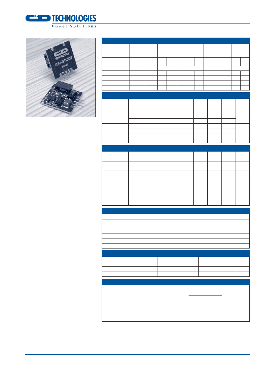
 | –≠–ª–µ–∫—Ç—Ä–æ–Ω–Ω—ã–π –∫–æ–º–ø–æ–Ω–µ–Ω—Ç: NGA | –°–∫–∞—á–∞—Ç—å:  PDF PDF  ZIP ZIP |

www.cdpoweronline.com
SELECTION GUIDE
1
FEATURES
Industry Standard Footprint
Short Circuit Protection
Efficiency to 95%
Wide Input Range
1.8V, 2.5V, 3.3V & 5V Output
Operating Temperature Range
≠40∞C to 85∞C
SMD Construction
Optional Shutdown & Trim Pins
DESCRIPTION
The NGA series is a range of low profile
DC/DC converters offering a single regulated
output over a wide input voltage range. All
parts deliver the full output power up to 85∞C
without the need for external heatsinking
while the synchronus rectification design
yields excellent efficiencies up to 95%.
Nominal Output
Output
Nominal
Power
Nominal
Input
Voltage
Current
Input Current
Consumption @ Efficiency
Voltage
@ Full Load
Shutdown
Min Full
Min Nom Max Min Nom Max Min Max
Load Load V
IN
V
IN
V
IN
V
IN
V
IN
V
IN
V
IN
V
IN
Order Code
(V)
(V)
A
mA
mW
%
NGA10S15018S
15
1.8
0
2.0 847 280 160 0.5 4.8 16.1 89
81
NGA10S15025S
15
2.5
0
2.0 1142 380 210 0.5 4.8 16.1 92
85
NGA10S15033S
15
3.3
0
2.0 1478 480 269 0.5 4.8 16.1 94
88
NGA10S15050S
2
15
5.0
0
2.0 1493 705 388 1.0 4.8 16.1 95
92
Parameter
Conditions
MIN
TYP
MAX
Units
Continuous operation
Voltage Range
1.8,2.5 & 3.3V output types
4.75
15
28
VDC
Continuous operation NGA10S15050S
7.0
15
28
Continuous operation NGA10S15050SE Variable
3
15
28
1.8V output types
29
Reflected Ripple 2.5V output types
49
mA p-p
Current
3.3V output types
48
5.0V output types
99
INPUT CHARACTERISTICS
1
OUTPUT CHARACTERISTICS
1
ABSOLUTE MAXIMUM RATINGS
NGA SERIES
Non-Isolated Wide Input DC/DC Converters
ENVIRONMENTAL
1
TERMINOLOGY
Parameter
Conditions
MIN
TYP
MAX
Units
Operation
≠ 40
85
∞C
Storage
≠ 50
125
∞C
PCB Temperature above Ambient
40
∞C
Parameter
Conditions
MIN
TYP
MAX
Units
Rated Power
T
A
= ≠40∞C to 85∞C
10
W
Voltage Set
±1.5
±5.0
%
Point Accuracy
Low line to high line,
Line Regulation with external input/output capacitors,
0.2
0.5
%/%
refer to test circuit
10% load to 100% load,
Load Regulation with external input/output capacitors,
1.5
2.0
%
refer to test circuit
BW = DC to 20MHz
Ripple & Noise With external input/output capacitors,
40
70
mVp-p
refer to test circuit
TRANSIENT RESPONSE
Time for V
OUT
to be within 1% of V
NOM
where V
NOM
=
V
OUT
25% +V
OUT
75%
2
OVER-SHOOT/UNDER-SHOOT
MAX deviation from final steady state output.
START DELAY
Typical rise time (ms) after control pin high with valid input.
1 Specifications typical at T
A
=25∞C, nominal input voltage and rated output current unless otherwise specified.
2. If optional VADJ and SD pin are required (as indicated in the mechanical dimensions diagram) suffix the part
number with an E when ordering, i.e. NGA10S15050SE.
3. Supply voltage should exceed output voltage by 1.45V.
Short circuit protection
Continuous
Internal power dissipation
1.1W
Lead temperature 1.5mm from case for 10 seconds
300∞C
Input Voltage V
IN
28V
Minimum load
0%
Output Trim Control
0V to +5V relative to 0V
Shutdown Control
≠0.3V to +28V relative to 0V

NGA SERIES
Non-Isolated Wide Input DC/DC Converters
GENERAL CHARACTERISTICS
1
Parameter
Conditions
MIN
TYP
MAX Units
Switching Frequency
270
300
330
kHz
50% load change, 1.8V output types
90(160)
Transient Response
50% load change, 2.5V output types
84(145)
MAX Over-Shoot
50% load change, 3.3V output types
83(130)
mV(µs)
50% load change, 5.0V output types
75(40)
50% load change, 1.8V output types
64(160)
Transient Response
50% load change, 2.5V output types
86(145)
MAX Under-Shoot
50% load change, 3.3V output types
84(120)
mV(µs)
50% load change, 5.0V output types
74(80)
Under Voltage
1.8, 2.5 & 3.3V output types
4.0
Lock Out
5.0V output types
5.0
V
Start Delay
V
IN
MIN to V
IN
MAX
100
ms
ESD
400VDC from 100pF capacitor
Meets MIL-STD-833E
via 1500 resistance
method 3015.7
Weight: 4.0g
0.825
(20.96)
0.1
(2.54)
0.846
(21.49)
MECHANICAL DIMENSIONS
0.877
(22.29)
0.22
(5.60)
0.014±0.002
(0.35±0.05)
0.02±0.002
(0.50±0.05)
0.312
(7.92)
4
5*
3
2
1*
2
1*
5*
3
4
0.161 (4.1)
3 Pin SIP Package Style
0.149
(3.78)
1 Specifications typical at T
A
=25∞C, nominal input voltage and rated output current
unless otherwise specified.
Unless otherwise stated all dimensions in inches(mm) ±0.01(0.25).
* Optional pins available on NGA10S15050SE only.
PIN CONNECTIONS
Pin Number
1*
2
3
4
5*
SD
V
IN
GND
V
OUT
V
ADJ
RECOMMENDED FOOTPRINT DETAILS
0.1
(2.54)
ÿ
0.057(1.45)
0.051(1.30)
0.1
(2.54)
ÿ 0.004(0.10)
All pins on a 0.1(2.54) pitch
and within 0.01(0.25) of true position.

NGA SERIES
Non-Isolated Wide Input DC/DC Converters
APPLICATION NOTES
EXTERNAL CAPACITANCE
External capacitors are necessary in
order to guarantee stability and full
parametric performance over the full line
and load range. All parts have
been tested and characterised using the
following values and test circuit.
TEST CIRCUIT
Value
1
C
IN
C
OUT
100µF, 50V
100µF, 10V
+
+
C
OUT
C
IN
V
IN
V
OUT
GND
GND
NGA
C&D Technologies (NCL) Ltd
Tanners Drive, Blakelands North
Milton Keynes MK14 5BU, England
Tel: +44 (0)1908 615232
Fax: +44 (0)1908 617545
email: info@cdtechno-ncl.com
www.cdpoweronline.com
C&D Technologies Inc.
3400 E Britannia Drive, Tucson,
Arizona 85706, USA
Tel: +1 (800) 547-2537
Fax: +1 (520) 741-4598
email: sales@cdtechno.com
C&D Technologies (NCL) Limited reserve the right to alter or improve the
specification, internal design or manufacturing process at any time, without
notice. Please check with your supplier or visit our web site to ensure that
you have the current and complete specification for your product before use.
© C&D Technologies (NCL) Limited 2003
NDC NGA.3
No part of this publication may be copied, transmitted or stored in a
retrieval system or reproduced in any way including, but not limited to,
photography, photocopy, magnetic or other recording means, without prior
written permission from C&D Technologies (NCL) Limited.
Instructions for use are available from www.cdpoweronline.com
1 Specifications typical at T
A
=25∞C, nominal input voltage and rated output current unless otherwise specified.
2 Accuracy of adjustment is subject to tolerance of resistors and initial output accuracy.
SHUTDOWN
When the shutdown pin is shorted to the
0V, the device's output will be disabled.
To shutdown the device the pin should be
taken below 0.8V using either an open
collector pull down or by using isolated
relay contacts. To enable the device
output the shutdown pin should be left
floating or taken no less than +1.5V to
MAX (+28V).
If the shutdown pin is to be connected to
a long wire, it is recommended that a
capacitor (10nF) decouples the shutdown
pin to the 0V in order to avoid the risk of
injecting noise into the device circuit.
VOLTAGE TRIMMING
The trimming (adjust) input on the device
allows output voltage adjustment to within
±5%
2
of the desired V
OUT
using a resistor
with a value determined by the following
equations.
When open circuit, the output will be +5V.
A resistor (R
D
) between the trim pin and
the output pin will adjust the output
voltage between +5V to +1.8V.
1 = (22(1.028V
O
≠1))
≠1
≠0.011
R
D
A resistor (R
U
) between the trim pin and
the 0V pin will adjust the device output
from +5V to +5.5V.
1 = (1.02V
O
)≠1
R
U
91
0.0455
NGA
NGA
OFF
ON
BC182 or equiv
10nF
(optional)
TTL
1K
V
IN
V
ADJ
SD
0V
V
OUT
R
D
NGA
V
IN
V
ADJ
SD
0V
V
OUT
R
U


