 | –≠–ª–µ–∫—Ç—Ä–æ–Ω–Ω—ã–π –∫–æ–º–ø–æ–Ω–µ–Ω—Ç: SLC100-1 | –°–∫–∞—á–∞—Ç—å:  PDF PDF  ZIP ZIP |
1
SLC100 1.2V Rev C 11/2004
Product: www.cdpoweronline.com
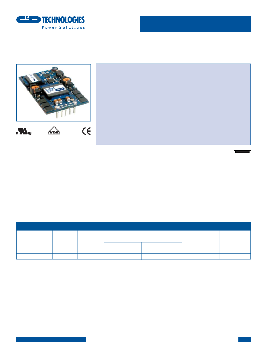
40 Amp Single Output Quarter Brick DC/DC Converter
SLC100
1.2V
Corporate: www.cdtechno.com
Corporate: www.cdtechno.com
Product: www.cdpoweronline.com
Industry Standard Footprint & Size -
2.28" x 1.45"
High Efficiency
Wide Input Voltage Range: 36 ≠ 75VDC
Series Output Voltage: 1.0V, 1.2V,
1.5V, 1.8V, 2.0V, 2.5V, 3.3V, 5.0V & 12V
Output VoltageTrim Function
Remote Sense for output
compensation
Remote ON/OFF control referenced to
input side (Positive or Negative Logic)
Output Current Limit
No Minimum Load Requirement
The SLC100 Series is a 40 Amp single
output, low-profile DC-DC converter
in an industry standard package of
2.28" x 1.45" x 0.40". The SLC100
uses unique proprietary technologies
to deliver ultra-high efficiencies and
excellent thermal performance. It includes
extensive control and protection features
for maximum fl exibility and satisfi es the
power requirements for a whole range of
applications with its input voltage range of
36-75 VDC and output voltages between
1.0VDC and 12.0VDC
The power dissipation of the SLC100
series is so low that a heat sink is not
required. Thermal derating curves are
provided indicating maximum allowable
output current versus airfl ow and ambient
temperature. The product features fast
dynamic response characteristics and
low output ripple critical for low voltage
applications. SLC DC-DC converter
modules are certifi ed to UL/CUL 60950,
and VDE EN60950. It meets CISPR22/
EN55022/FCC15J Class B specs for EMI
levels with external fi ltering.
This high quality and highly reliable
product is competitively priced and an
ideal solution for distributed power,
telecoms and datacom applications.
ISO9001
CERTIFIED
* Note 1: Maximum output current for SMD Models is 25A.
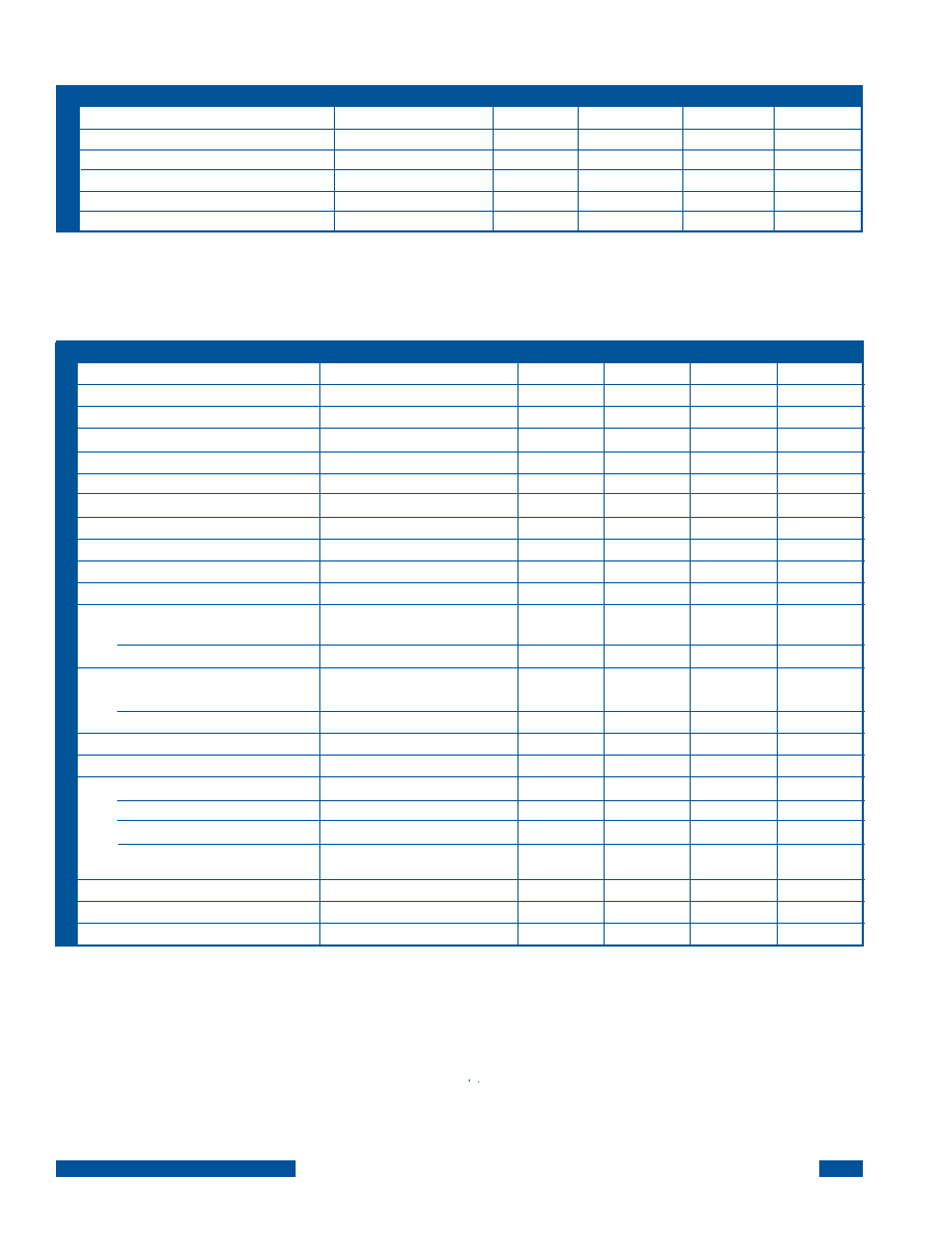
NOMINAL
RATED
INPUT
OUTPUT
OUTPUT CURRENT
VOLTAGE
VOLTAGE
MIN
RATED
MODEL (V
DC
) (V
DC
) LOAD(A)
OUTPUT
(A)
1
SLC100-2,11,20,29 48
1.2
0.0
40
1.30
80
PRODUCT SELECTION CHART
INPUT
CURRENT
AT RATED LOAD (A)
(48Vin)
EFFICIENCY
TYPICAL
(%)
SMD Models with Position Perfect
TM
Interconnects
Isolation Voltage of 2000 VDC
Fixed Frequency Operation
UL/CUL 60950 recognized (US & Canada),
VDE EN60950, basic insulation rating
Meets TNV-SELV Isolation Requirements
Meets Conducted Emissions
Requirements of FCC Class B and
EN55022 Class B with External Filter
No Heatsink Required
Thermal Shutdown
Input Undervoltage Lockout
2
SLC100 1.2V Rev C 11/2004
Product: www.cdpoweronline.com
ABSOLUTE MAXIMUM RATINGS, ALL MODELS
PARAMETER CONDITIONS
MIN
TYP
MAX
UNITS
COMMON ELECTRICAL SPECIFICATIONS, ALL MODELS
Specifications are at T
A
= +25∞C, Airflow = 300LFM (1.5m/s) at nominal input voltage unless otherwise specified.
Input Voltage-Operating
Input Voltage-Operating
Operating Ambient Temperature
Storage Temperature
Output Short Circuit Duration
Lead Temperature (Soldering, 10 sec max)
Continuous
75
V
DC
Continuous
Transient (100 mS)
100
V
DC
-40 85
∞C
∞C
-40 +125
+300
∞C
PARAMETER CONDITIONS
MIN
TYP
MAX
UNITS
INPUT
Voltage Range
36
48
75
V
DC
ISOLATION
Input/Output Isolation Voltage
2000
V
DC
Capacitance
Input to Output
2000
pF
Resistance
Input to Output
10
M
FEATURES
Turn On Time
Output to within 1% of Vnom
5.00
mS
Remote Sense Compensation
5
% of V
NOM
Output Voltage Trim Range
-10
+10
% of V
NOM
Output Over Voltage Protection
+120
+140
% of V
NOM
Over Temperature Shutdown
Shutdown
Internal
Monitor
Point 135 ∞C
Turn On
Internal Monitor Point
125
∞C
Input Under Voltage Protection
Turn
Off
30.70 32.00
V
DC
Turn
On
33.30 34.50
V
DC
Lockout Hysteresis Voltage
1.30 2.50
V
DC
ON/OFF Logic Function
Logic Low Ion/off
360
A
Logic Low Von/off
0.4
V
DC
Logic
High
Ion/off
1.0
A
Logic
High
Von/off
Open
Collector
GENERAL
Switching Frequency
200
KHz
MTTF (per Telcordia TR-332)
1,497,000
Hrs
COMMON ELECTRICAL
SPECIFICA
TIONS
3
SLC100 1.2V Rev C 11/2004
Product: www.cdpoweronline.com
MECHANICAL (THROUGH HOLE)
NOTES:
General Tolerance:
±
.015
Pin Locations/Diameters:
±
.005
Dimensions are in inches
[Millimeters]
Pin material: Copper
Pin Finish: Matte Tin over Nickel
Converter weight: [30.8g]
MECHANICAL (SMT)
PIN FUNCTIONS
1
+Vin
2 Remote
On/Off
3
-Vin
4
-Vout
5
-
Sense
6
Trim
7
+
Sense
8
+Vout
Interconnect FUNCTIONS
1
+Vin
2 Remote
On/Off
3
-Vin
4
-Vout
5
-
Sense
6
Trim
7
+
Sense
8
+Vout
* Interconnect co-planarity within 0.004"
UL/TUV Standards require a clearance
greater than 0.04" between input and
output for Basic insulation. This should be
considered if copper traces are used on
the top side of the board under the con-
verter unit. Ferrite cores are considered
part of the input/primary circuit.
UL/TUV Standards require a clearance
greater than 0.04" between input and
output for Basic insulation. This should be
considered if copper traces are used on
the top side of the board under the con-
verter unit. Ferrite cores are considered
part of the input/primary circuit.
NOTES:
General Tolerance:
±
.015
Interconnect Locations/
Diameters:
±
.005
Dimensions are in inches
[Millimeters]
Pin material: Copper
Pin Finish: Matte Tin over Nickel
Converter weight: [30.8g]
.425
[10.80]
.725
[18.42]
1.025
[26.04]
1.025 [26.04]
.875 [22.23]
.725 [18.42]
.575 [14.61]
.425 [10.80]
.000 [0.00]
.000 [0.00]
2.280 [57.91]
1.450
[36.83]
.140 [3.56]
2.140 [54.36]
.400
[10.16]
.197 [5.00]
2x, ÿ.060 [1.52]
6x, ÿ.040 [1.02]
BOTTOM VIEW
(PIN SIDE)
.052
[1.32]
.037
[0.94]
2x, ÿ080 [2.03]
6x, ÿ.060 [1.52]
3
1
2
5
6
7
8
4
.425
[10.80]
.725
[18.42]
1.025
[26.04]
1.025 [26.04]
.875 [22.23]
.725 [18.42]
.575 [14.61]
.425 [10.80]
.000 [0.00]
.000 [0.00]
2.280 [57.91]
1.450
[36.83]
.140 [3.56]
2.140 [54.36]
.400
[10.16]
BOTTOM VIEW
(PIN SIDE)
.052
[1.32]
.037
[0.94]
4
2x, ÿ.080 [2.03]
6x, ÿ.060 [1.52]
3
2
5
6
7
8
1
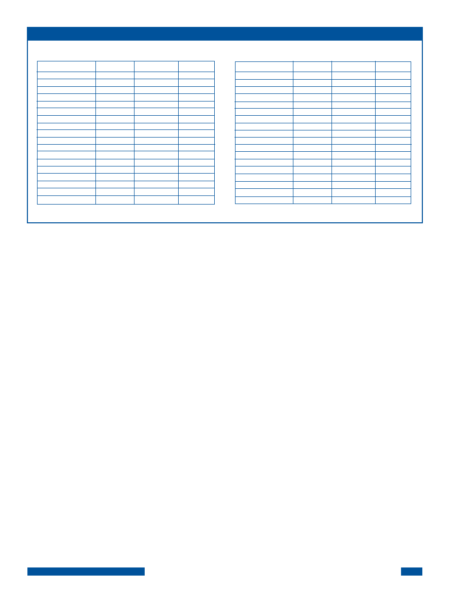
4
SLC100 1.2V Rev C 11/2004
Product: www.cdpoweronline.com
ORDERING INFORMATION
MODEL NUMBER Vout (Vdc) PINOUT LOGIC
SLC100 - 1 1.0 Through Hole Positive
SLC100 - 2 1.2 Through Hole Positive
SLC100 - 3 1.5 Through Hole Positive
SLC100 - 4 1.8 Through Hole Positive
SLC100 - 5 2.0 Through Hole Positive
SLC100 - 6 2.5 Through Hole Positive
SLC100 - 7 3.3 Through Hole Positive
SLC100 - 8 5.0 Through Hole Positive
SLC100 - 9 12.0 Through Hole Positive
SLC100 - 10 1.0 SMD Positive
SLC100 - 11 1.2 SMD Positive
SLC100 - 12 1.5 SMD Positive
SLC100 - 13 1.8 SMD Positive
SLC100 - 14 2.0 SMD Positive
SLC100 - 15 2.5 SMD Positive
SLC100 - 16 3.3 SMD Positive
SLC100 - 17 5.0 SMD Positive
SLC100 - 18 12.0 SMD Positive
MODEL NUMBER Vout (Vdc) PINOUT LOGIC
SLC100 - 19 1.0 Through Hole Negative
SLC100 - 20 1.2 Through Hole Negative
SLC100 - 21 1.5 Through Hole Negative
SLC100 - 22 1.8 Through Hole Negative
SLC100 - 23 2.0 Through Hole Negative
SLC100 - 24 2.5 Through Hole Negative
SLC100 - 25 3.3 Through Hole Negative
SLC100 - 26 5.0 Through Hole Negative
SLC100 - 27 12.0 Through Hole Negative
SLC100 - 28 1.0 SMD Negative
SLC100 - 29 1.2 SMD Negative
SLC100 - 30 1.5 SMD Negative
SLC100 - 31 1.8 SMD Negative
SLC100 - 32 2.0 SMD Negative
SLC100 - 33 2.5 SMD Negative
SLC100 - 34 3.3 SMD Negative
SLC100 - 35 5.0 SMD Negative
SLC100 - 36 12.0 SMD Negative

5
SLC100 1.2V Rev C 11/2004
Product: www.cdpoweronline.com
Figure 1 ≠ Remote Sensing Circuit
Output Voltage Trim
The SLC100's output voltage may be adjusted high
or low by an amount indicated on the product data
sheet. As shown in Figure 2, to raise the converter's
output voltage a resistor must be placed between the
Trim pin and +Vout pin.
Figure 2 ≠ Trim Up Circuit
Remote Sense
Operation
When the load is physically distanced from the con-
verter, the inductance of the power leads, and any by-
pass conductance at the load, can result in increased
phase shift in the converter's feedback loop, causing
instability. This situation can be eliminated by insert-
ing bypass capacitors (C
B
) from the outputs to the
sense leads directly at the output pins. These capaci-
tors de-couple any AC on the power lines and assure
that only the DC voltage is sensed.
When using remote sense with dynamic loads, the
transient response at the point of load may be limited
by the inductance present in the power lines. Severe
load steps may require the addition of a capacitor
C
L
across the output lines. When the load demands
an immediate increase in load current, this capacitor
helps to supply a portion of the current and reduces
the burden on the converter.
In general, the line resistance, or load drop, between
the output pins of the converter and load should be
minimized. Using remote sense, a large line resis-
tance, with a regulated load voltage, will result in
a higher output voltage at the output of the DC/DC
Converter. To prevent exceeding the converter's
output power limits, a higher output voltage will
require a reduction in the maximum allowable output
current in accordance with the voltage/current power
relationship. To minimize the line resistance between
the converter and the load, the converter should be
placed as close to the load as possible. Line resis-
tance can further be decreased by using heavy gauge
wire or by increasing the cross sectional area of the
PC board traces.
The remote sense feature of the SLC100 can be used
to compensate for voltage drops in the output power
lines by sensing output voltage directly at the point of
load. To enable this feature, connect the +Sense and
≠Sense pins to the +Vout and ≠Vout pins, respective-
ly, at the point in the circuit where the tightest regula-
tion is required (Figure 1). The sense leads conduct
very little current compared with the power leads and
therefore provide a more accurate indication of load
voltage for regulation purposes. This enables the
converter to increase (or decrease) its output volt-
age to compensate for any load distribution losses,
allowing for a more precise load voltage. Refer to the
product data sheet for the maximum output voltage
compensation range of the sense function.
APPLICATION NOTES
If remote sensing is not desired then +Sense and
-Sense must be tied to their respective outputs
for proper operation.
∑
∑