SUPERSIP26 11/99 REV C
Page 1
Product Data Sheet
5 V
DC
I
NPUT
, 3.3 V
DC
O
UTPUT
DC/DC C
ONVERTER
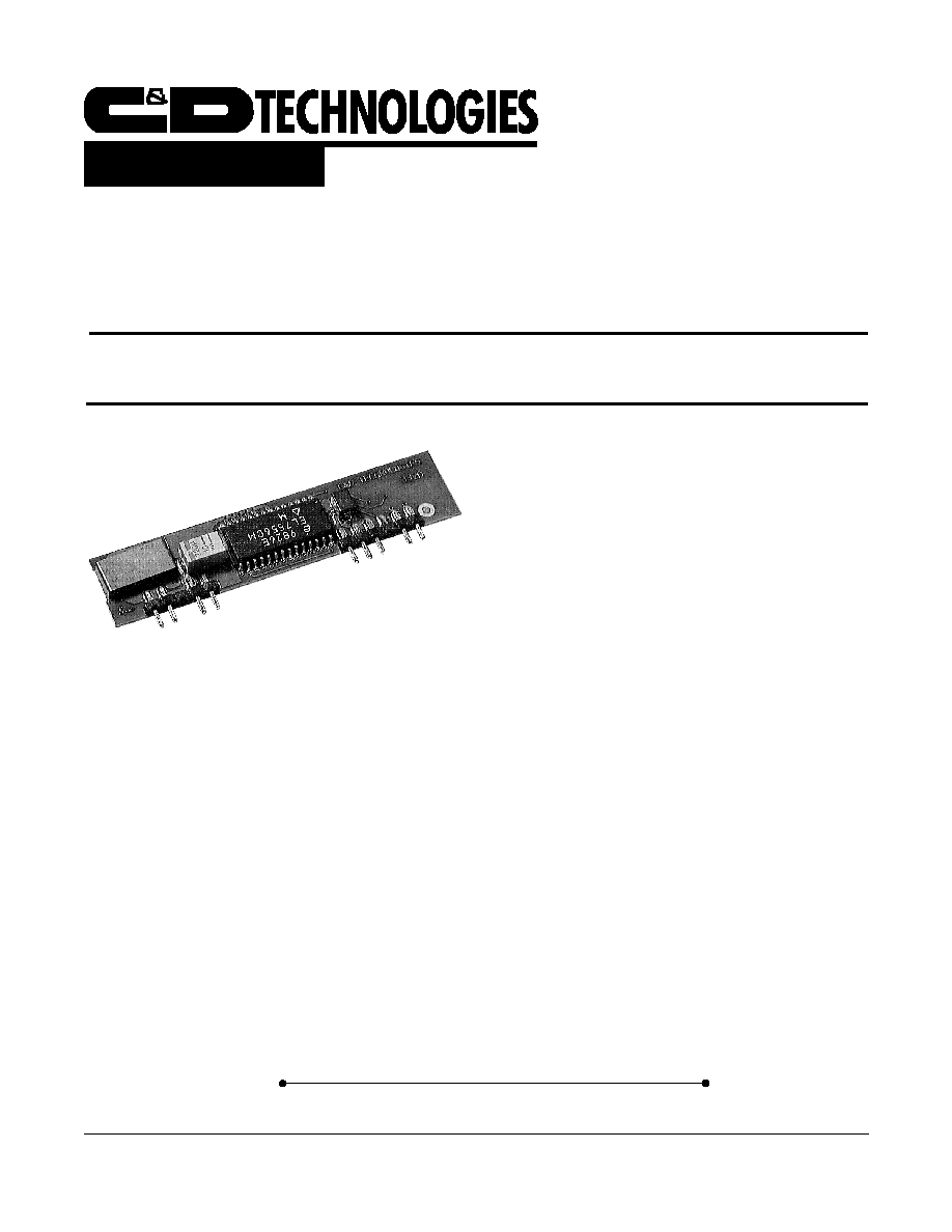
SS26 (SuperSIP
SS26 (SuperSIP
SS26 (SuperSIP
SS26 (SuperSIP
SS26 (SuperSIP
T
T
T
T
TM
M
M
M
M
))
)))
Features
q
Non isolated DC/DC Converter designed to
operate from a regulated 5V bus
q
Output voltage Range: 1.8V - 3.6V
q
Easy resistive programming for desired output
q
No resistive programming gives 3.3 Vdc output
q
Wave solderable
Description
The SS26 (SuperSIP
TM
) DC/DC converter accepts a
regulated 5V input (�10%) and provides 1.8Vdc to 3.6Vdc
at 6A. The circuit is optimized for high efficiency and fast
load transient response needed by telecom, DSP, and
microprocessor applications. Advanced thermal design,
monolithic power circuitr y, planar magnetics, and
synchronous rectification result in outstanding
performance and value. Pins are staked for wave
solderability. Multiple programming, power good and on/
off options allow superior flexibility and drop in compatibility
for most existing designs.
Internet: http://www.cdpowerelectronics.com
Power Electronics Division, United States
3400 E Britannia Drive, Tucson, Arizona 85706
Phone: 520.295.4100 Fax: 520.770.9369
Power Electronics Division, Europe
C&D Technologies (Power Electronics) Ltd.
132 Shannon Industrial Estate
,
Shannon, Co. Clare, Ireland
Tel: +353.61.474.133
Fax:+353.61.474.141
More product information and application notes are available
on our website at www.cdpowerelectronics.com
SUPERSIP26 11/99 REV C
Page 2
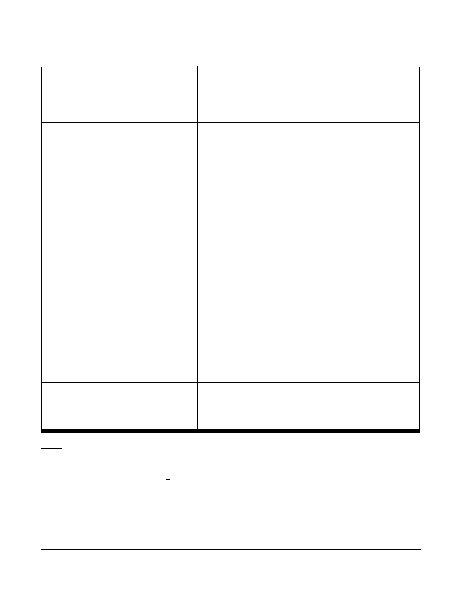
Electrical Specifications
Unless otherwise specified, operating conditions are as follows: V
in
=5V, V
o
=3.3V, I
o
=6A, T
A
=25�C, C
in
=100
�
F, C
o
=0F.
Notes
1.
Input source<3" from SuperSIPTM, Load transient <3A per SIP. 100
�
F low ESR capacitor for load transients
>3A.
2.
Optional programming 1.8 - 3.6 or +10% available. See Table.
3.
100 lfm air, V
o
=3.3V, I
o
=6A. See Thermal Design Guide for other conditions.
Parameters
Conditions
Min.
Typ.
Max.
Units
Input
Input Voltage
V
in
4.5
5.0
5.5
V
DC
Input Current Ripple
200
mA
RMS
Required Capacitance
C
in
Note 1
0
100
�
F
Output
Output Voltage
V
o
Nominal
3.25
3.3
3.35
V
DC
Output Program Range
Note 2
1.8
3.6
V
DC
Output Current
I
o
T
A
=25�C
0
6
Amps
Output Ripple
20 Mhz BW
15
50
mVp-p
Output Rise time
T
700
�
S
Output Capacitance Range
C
o
0
5000
�
F
Line Regulation
�0.5
%
Load Regulation
I
o
min-I
o
max
�1.0
%
Temperature Coefficient
T
c
0.01
%/�C
Combined variation
V
in
min-max
I
o
min-max
T
A
=25C�-85C�
-2
+2
%
Current Limit
I
limit
V
in
= 4.75Vdc
6.5
9
12
A
General
Switching Frequency
800
kHz
Dynamic Response
I
O
/
t = 1A/1 0
!
sec, V
i
= 5.0V, T
A
= 25�C
Load Change from I
O
= 0% to I
O
= 100%
Peak Deviation
30
mV
Settling time (V
O
<10% Peak Deviation)
100
�
sec
Load change from I
O
= 100% to I
O
= 0%
Peak Deviation
30
mV
Settling time (V
O
<10% Peak Deviation)
100
�
sec
Temperature
Operating Temperature
Note 3
0
+60
�C
Storage Temperature
-40
+125
�C
SUPERSIP26 11/99 REV C
Page 3
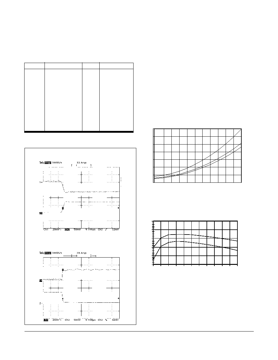
Thermal Design Guide
Locate your operating current, read the junction temp
rise from the graph and add to your maximum ambient.
135�C is the maximum allowable operating junction tem-
perature. Test conditions: Device soldered into 4" x 4"
PCB, 2 sided with power and ground planes for heat con-
duction. Due to the difficulty in predicting the thermal
effects of airflow velocity and direction, and thermal con-
duction through ground planes it is important that the SS26
SuperSIP
TM
be evaluated thermally in each application.
For high ambient temperature/high current application
please request our Application Note 35-118-01, "Accurate
Measurements of SS26 SuperSIP
TM
Junction Tempera-
ture", for further assistance.
Programming
To program the SS26 SuperSIP
TM
for V
out
<3.3, connect
resistor across pins 8 (TRIM) and 1(V
o
). For V
out
>3.3, re-
sistor is connected across pins 8 and 4 (Gnd).
T
j
Rise vs. I
o
(Junction Temp Rise vs. Output Current)
EFFICIENCY %
OUTPUT CURRENT AMPS
V
o
=3.3V, C
out
-O
�
f, V
i
=5V, C
in
=100
�
f
Efficiency
100
95
90
85
80
75
0.5 1.5 2.5 3.5 4.5 5.5
T
emp Rise C
OUTPUT CURRENT - AMPS
70
60
50
40
30
20
10
0
0.5
1
1.5
2
2.5
3
3.5
4
4.5
5
5.5
6
STILL
AIR
100LFM
300LFM
3.3V 25C
2.1V 25C
Table 2
V
out
Resistor Value
V
out
Resistor Value
1.8
576
2.8
18.2k
1.9
1.21k
2.9
24.3k
2.0
1.96k
3.0
34.8k
2.1
2.8k
3.1
54.9k
2.2
3.83k
3.2
110.0k
2.3
4.99k
3.3
OPEN
2.4
6.49k
3.4
66.5k
2.5
8.25k
3.5
29.4k
2.6
10.7k
3.6
18.2k
2.7
13.7k
Transient Response
Operating conditions are as follows: Vin=5V, Vo=3.3V, Load
change from Io=0% to Io=100%, TA=25�C, Cin=0F, Co=
�
F.
Operating conditions are as follows: Vin=5V, Vo=3.3V, Load
change from Io=100% to Io=0%, TA=25�C, Cin=0F, Co=
�
F.
SUPERSIP26 11/99 REV C
Page 4
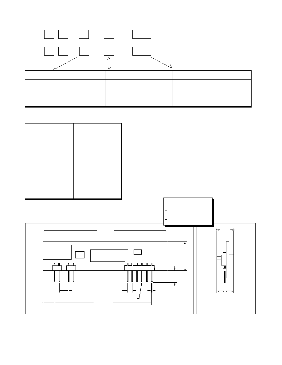
Ordering Information
Typical examples:
Pin Out
Pin
Function
Description
1
V
o
Output Voltage
2
V
o
Output Voltage
3
V
o
Output Voltage
4
GND
Ground
5
GND
Ground
6
V
IN
Input Voltage
7
V
IN
Input Voltage
7A
P
good
Power Good Option
8
Trim
Output Voltage Adjust
9
Enable
Enable Option
The information provided herein is believed to be reliable; however, C&D TECHNOLOGIES assumes no responsibility for inaccuracies or omissions. C&D TECHNOLOGIES
assumes no responsibility for the use of this information, and all use of such information shall be entirely at the user's own risk. Prices and specifications are subject to change
without notice. No patent rights or licenses to any of the circuits described herein are implied or granted to any third party. C&D TECHNOLOGIES does not authorize or warrant
any C&D TECHNOLOGIES product for use in life support devices/systems or in aircraft control applications.
Power Good
Enable
Programming (See Table 2)
A = Pin 7A installed for Power
A = logic1 or open = ON
A = Standard 3.3V with Pin 8 open
Good option
logic 0 or gnd = OFF
or program per Table 2.
B = Pin omitted (industry standard)
B = logic 0 or gnd = ON
logic 1 = OFF
Mechanical
TOLERANCES
+.008" for 3 place decimals
+ .02" for 2 place decimals
+ .002" for pin diameter
.14 (3.56)
0.28 (7.2)
1 2 3
4
2.50 (63.5)
1.900 (48.26)
.200 (5.08)
0.025 (64)
SQUARE TIP
OPTIONAL
0.100 (2.54)
0.55 (14.0)
0.14
(3.56)
0.30
(7.62)
.16 (4.06)
5 6 7 7A 8 9
SS
26
-
A
-
A
-
A
Standard configuration 5V to 3.3V
with 1.8V-3.6V trim range
SS
26
-
B
-
A
-
A