
WP05R 5/98 REV B
Page 1
FEATURES
SMALL PACKAGE SIZE: 1" X 2"
INDUSTRY STANDARD PINOUT
SURFACE MOUNT DEVICES (SMD)
LOW-COST ALTERNATE SOURCE
CONTINUOUS SHORT CIRCUIT PROTECTION
UL1950 RECOGNITION
(SOME MODELS PENDING)
MEETS FCC CLASS B
APPLICATIONS
TELECOMMUNICATION EQUIPMENT
BATTERY POWERED SYSTEMS
PORTABLE INSTRUMENTS
PROCESS CONTROL EQUIPMENT
TRANSPORTATION EQUIPMENT
DISTRIBUTED POWER SYSTEMS
SPACE-CRITICAL APPLICATIONS
DESCRIPTION
The WP05R Series is a family of high performance DC/DC
converters that offer high efficiency and regulated outputs
over a 2:1 input voltage range of either 18-36VDC or 36-
72 VDC.
Surface mount devices and manufacturing technology make
it possible to offer performance equivalent to competition
at a lower cost.
A self oscillating flyback topology coupled with a rugged
MOSPOWER transistor are used to produce a highly reli-
able product with a minimum parts count. The internal
body diodes of these FETS protect the unit against input
voltage reversal. An external fuse is required to limit the
body diode current to 2 amps.
The WP05R Series offers low noise (approximately 50 to
75mVp-p) without the addition of an external capacitor.
The series is also 6-sided shielded, further reducing
system noise. This shield is connected to -VIN.
No external heatsink is required for the WP05R Series
to supply its rated 5 watts. With a minimum amount of
airflow, the temperature range may be extended from
70�C to 85�C. (See derating curve.)
The package of the WP05R Series is plastic. This
eliminates the layout precautions required by metal
enclosed devices. The encapsulant material is rated
UL94V-0 for flammability and offers excellent heat
transfer characteristics.
Internal circuitry provides continuous short-circuit pro-
tection and automatic restart after the short is removed.
5 W
ATT
R
EGULATED
S
MALL
P
ACKAGE
DC/DC C
ONVERTER
Product Data Sheet
3400 E Britannia Drive
Tucson, Arizona 85706 Phone: 520.295.4100 Fax: 520.770.9369 Internet: http://www.cdpowerelectronics.com
WP05R

WP05R 5/98 REV B
Page 2
PARAMETER
CONDITIONS
MIN TYP
MAX
UNITS
INPUT
Voltage Range
18
24
36
VDC
36
48
72
VDC
Reflected Ripple Current
20
35
mAp-p
ISOLATION
Rated Voltage
500
VDC
Test Voltage
60 Hz, 10 Seconds 500
Vpk
Resistance
10
G
Capacitance
470
pF
Leakage Current
V
ISO
= 240VAC, 60Hz
50
�Arms
OUTPUT
Rated Power
5.0
W
Voltage Setpoint Accuracy
Singles
�1
�2
%
Duals
�2
�4
%
Temperature Coefficent
�0.02
%/�C
Line Regulation
Low Line to High Line
Singles
5
mV
Duals
1
%
Load Regulation
Min Load to Rated Load
Singles
25
mV
Duals
1
%
Ripple and Noise
24VIN Models
BW = 20Hz to 10MHz
100
mVp-p
48VIN Models
BW = 20Hz to 10MHz
50
mVp-p
5V Output Models
BW = 20Hz to 2MHz
5
mVrms
Other Models
BW = 20Hz to 2MHz
10
mVrms
Transient Response
Rated Load to Min Load
10
mS
Min Load to Rated Load
10
mS
Overvoltage Protection Threshold
3.3V Output
3.9
VDC
5V Output
6.8
VDC
12V Output
15
VDC
15V Output
18
VDC
GENERAL
Switching Frequency
140
KHz
Package Weight
30
g
MTTF per MIL-HDBK-217
Ground Benign, Circuit Stress Method
Revision F
T
A
= +25�C
636,843
Hr
T
A
= +70�C
199,000
Hr
T
A
= +85�C
122,009
Hr
MTTF per Bellcore TR-NWT-000322
Environmental Stress = 1.0
Issue 4, September, 1992
T
A
= +25�C
1,079,617
Hr
T
A
= +70�C
205,055
Hr
T
A
= +85�C
98,839
Hr
TEMPERATURE
Specification
No Power Derating -40
+70
�C
Operation
-40
+100
�C
Storage
-55
+110
�C
COMMON SPECIFICATIONS
Specifications typical at T
A
= +25�C, nominal input voltage, rated output current unless otherwise specified.
ELECTRICAL SPECIFICATIONS
Specifications typical at T
A
= +25�C, nominal input voltage, rated output current unless otherwise specified.
NOMINAL
RATED OUTPUT CURRENT
INPUT CURRENT
INPUT
OUTPUT
VOLTAGE
VOLTAGE
MIN LOAD
RATED LOAD
MIN LOAD
RATED LOAD
EFFICIENCY
MODEL
(VDC) (VDC)
(mA)
(mA)
(mA)
(mA)
(%)
WP05R24S03
24
3.3
25
1500
20
300
70
WP05R24S05
24
5
50
1000
20
265
78
WP05R24S12
24
12
21
417
20
255
82
WP05R24S15
24
15
17
333
20
250
83
WP05R24D05
24
�5
�25
�500
20
265
78
WP05R24D12
24
�12
�10
�208
20
255
82
WP05R24D15
24
�15
�8
�167
20
250
83
WP05R48S03
48
3.3
25
1500
13
150
70
WP05R48S05
48
5
50
1000
13
135
78
WP05R48S12
48
12
21
417
13
127
82
WP05R48S15
48
15
17
333
13
125
83
WP05R48D05
48
�5
�25
�500
13
135
78
WP05R48D12
48
�12
�10
�208
13
127
82
WP05R48D15
48
�15
�8
�167
13
125
83
NOTE: Other input and output voltages may be available. Please consult factory.

WP05R 5/98 REV B
Page 3
For maximum safety and system protection, a Buss
PC-TRON, PCB 2A fuse or equivalent should be used
in series with the input.
FUSING
ABSOLUTE MAXIMUM RATINGS
Output Short-Circuit Duration.............................................................Continuous
Case Temperature .....................................................................................100�C
Lead Temperature (soldering, 10 seconds max).....................................+300�C
ORDERING INFORMATION
Device Family
Indicates Wide Input Power 5 Watt Regulated Unit
Model Number
Selected From Table of Electrical Characteristics
Where:
xx = Input Voltage
y = Number of Outputs (Single "S", Dual "D")
zz = Output Voltage
Package Option
Screening Option
WP05R xxyzz N /H
6
5
2.5W
2
1
0
-25
25
50
70�C
75
85�C
100
125
3
NATURAL
CONVECTION
Output Power (W
atts)
Ambient Temperature (�C)
POWER DERATING
500
LFM
AIRFLOW
4
APPLICATION NOTES
2.000�0.015"
(50.80�0.38)
1.000�0.015"
(25.4�0.38)
0.015�.005"
(0.38)
0.170"
(4.32)
0.400�0.10"
(10.16)
Min.
0.040�0.003"
(1.02�0.08)
-V
IN
+
V
IN
+V
OUT
-V
OUT
*
COM
MECHANICAL
BOTTOM VIEW
MATERIAL: Units are encapsulated in a low thermal resistance molding
compound which has excellent chemical resistance, wide operating tem-
perature range, and good electrical properties under high humidity environ-
ments. The encapsulant and the outer shell of the unit have UL94V-0
ratings. Lead material is brass with a solder plated surface to allow ease of
solderability.
PIN PLACEMENT TOLERANCE: �0.015 inches.
NOTES: All dimensions are in inches (millimeters).
GRID: 0.100 inches (2.54 millimeters)
*
Common pins are not present on single output
models.
Product marked with specific model ordered, date
code, job code.
SIDE VIEW
TOP VIEW
WP05R 5/98 REV B
Page 4
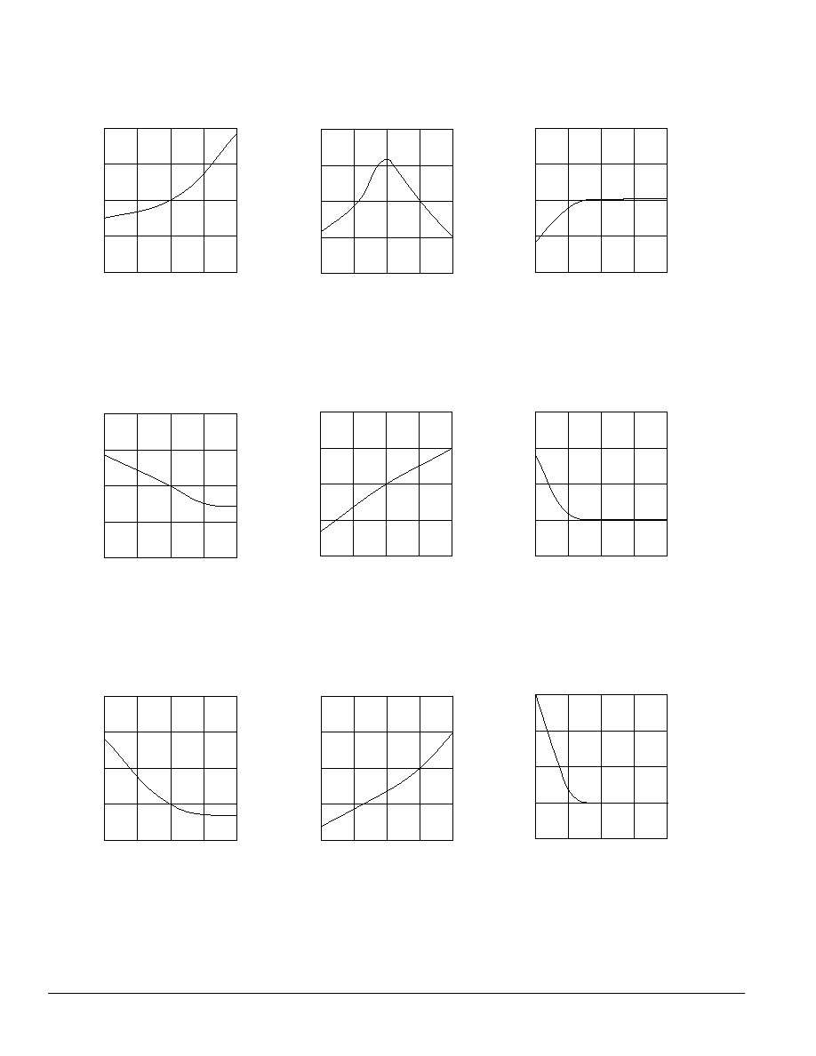
TYPICAL PERFORMANCE CURVES
T
A
= +25�C, nominal input voltage, rated load, recommended external components applied, unless otherwise specified.
REFLECTED RIPPLE CURRENT
vs INPUT VOLTAGE
REFLECTED RIPPLE CURRENT
vs OUTPUT LOAD
REFLECTED RIPPLE CURRENT
vs TEMPERATURE
OUTPUT NOISE vs INPUT VOLTAGE
OUTPUT NOISE vs OUTPUT LOAD
OUTPUT NOISE vs TEMPERATURE
EFFICIENCY vs INPUT VOLTAGE
EFFICIENCY vs OUTPUT LOAD
EFFICIENCY vs TEMPERATURE
Low
Line
Nom
Line
High
Line
Low
Line
Nom
Line
High
Line
Low
Line
Nom
Line
High
Line
Vin
Vin
Vin
Output Load (% of Rated)
Output Load (% of Rated)
Output Load (% of Rated)
T
A
(�C)
T
A
(�C)
T
A
(�C)
-40 -5 +25 +55 +85
-40 -5 +25 +55 +85
Change in Efficiency (%)
Change in Efficiency (%)
Change in Efficiency (%)
Change in Output Noise (%)
Change in Output Noise (%)
Change in Output Noise (%)
Change in Reflected Ripple Current (%)
Change in Reflected Ripple Current (%)
Change in Reflected Ripple Current (%)
+2%
TYP
-2%
-4%
-6%
+10%
+5%
TYP
-5%
-10%
+20%
+10%
TYP
-10%
-20%
+1`50%
+100%
+50%
TYP
-50%
+300%
+200%
+100%
TYP
-100%
+30%
TYP
-30%
-60%
-90%
+30%
TYP
-30%
-60%
-90%
+150%
+100%
+50%
TYP
-50%
-40 -5 +25 +55 +85
25% 44% 63% 82% 100%
25% 44% 63% 82% 100%
25% 44% 63% 82% 100%
+9%
+6%
+3%
TYP
-3%
The information provided herein is believed to be reliable; however, C&D TECHNOLOGIES assumes no responsibility for inaccuracies or omissions. C&D TECHNOLOGIES assumes
no responsibility for the use of this information, and all use of such information shall be entirely at the user's own risk. Prices and specifications are subject to change without notice.
No patent rights or licenses to any of the circuits described herein are implied or granted to any third party. C&D TECHNOLOGIES does not authorize or warrant any C&D TECHNOLOGIES
product for use in life support devices/systems or in aircraft control applications.