WPC03R 2/99 REV A
Page 1
3 W
ATT
R
EGULATED
W
IDE
I
NPUT
R
ANGE
DC/DC C
ONVERTER
FEATURES
l
Low Cost, High Performance
l
Small DIP Package
l
Full Power to +85∞C
l
Extended Temperature Range: -40∞C to +85∞C
l
Industry Standard Pinouts
l
Full Short Circuit Protection
l
High Capacitive Loading Capability
l
Protected Against High Input Voltage
DESCRIPTION
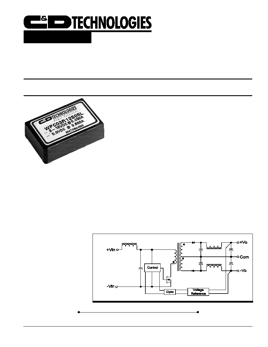
The WPC03R is a family of high performance DC/DC converters
that offers regulated outputs over input voltage ranges of 9-18V,
18-36V and 34-72V while offering a wide operating temperature
range of -40∞C to +85∞C without derating.
Each WPC03R contains input filtering to minimize conducted
noise. The design utilizes surface mounted components,
including magnetics, to provide enhanced reliability.
The converter is designed to meet the requirements of EN60950
with the "L" pinout having 1,500 V
DC
isolation. All WPC03R
converters are designed to withstand input voltage transients to
200% of nominal input voltage. An additional feature is the
ability of the WPC03R to drive high capacitive loads.
Internet: http://www.cdpowerelectronics.com
Power Electronics Division, United States
3400 E Britannia Drive, Tucson, Arizona 85706
Phone: 800.547.2537 Fax: 520.770.9369
Power Electronics Division, Europe
C&D Technologies (Power Electronics) Ltd.
132 Shannon Industrial Estate
,
Shannon, Co. Clare, Ireland
Tel: +353.61.474.133
Fax:+353.61.474.141
WPC03R
WPC03R
WPC03R
WPC03R
WPC03R
SIMPLIFIED CIRCUIT SCHEMATIC
APPLICATIONS
l
Telecommunications
l
Battery Powered Systems
l
Portable Instruments
l
Transportation Equipment
l
Distributed Power Systems
Product Data Sheet
WPC03R 2/99 REV A
Page 2
Output Short Circuit Protection ------------ Continuous
Internal Power Dissipation --------------------------- 1.5W
Lead Temp (soldering, 10s Max) ---------------- +300∞C
Max Case Temperature --------------------------- +100∞C
ABSOLUTE MAXIMUM RATINGS
ORDERING INFORMATION
WPC03R xxyzz E
Device Family
Indicates wide input power 3W regulated DC/DC
Model Number
Selected from Table of Electrical Characteristics
xx=input voltage
y=number of outputs: S=single, D=dual
zz=output voltage
Pinout option E or L
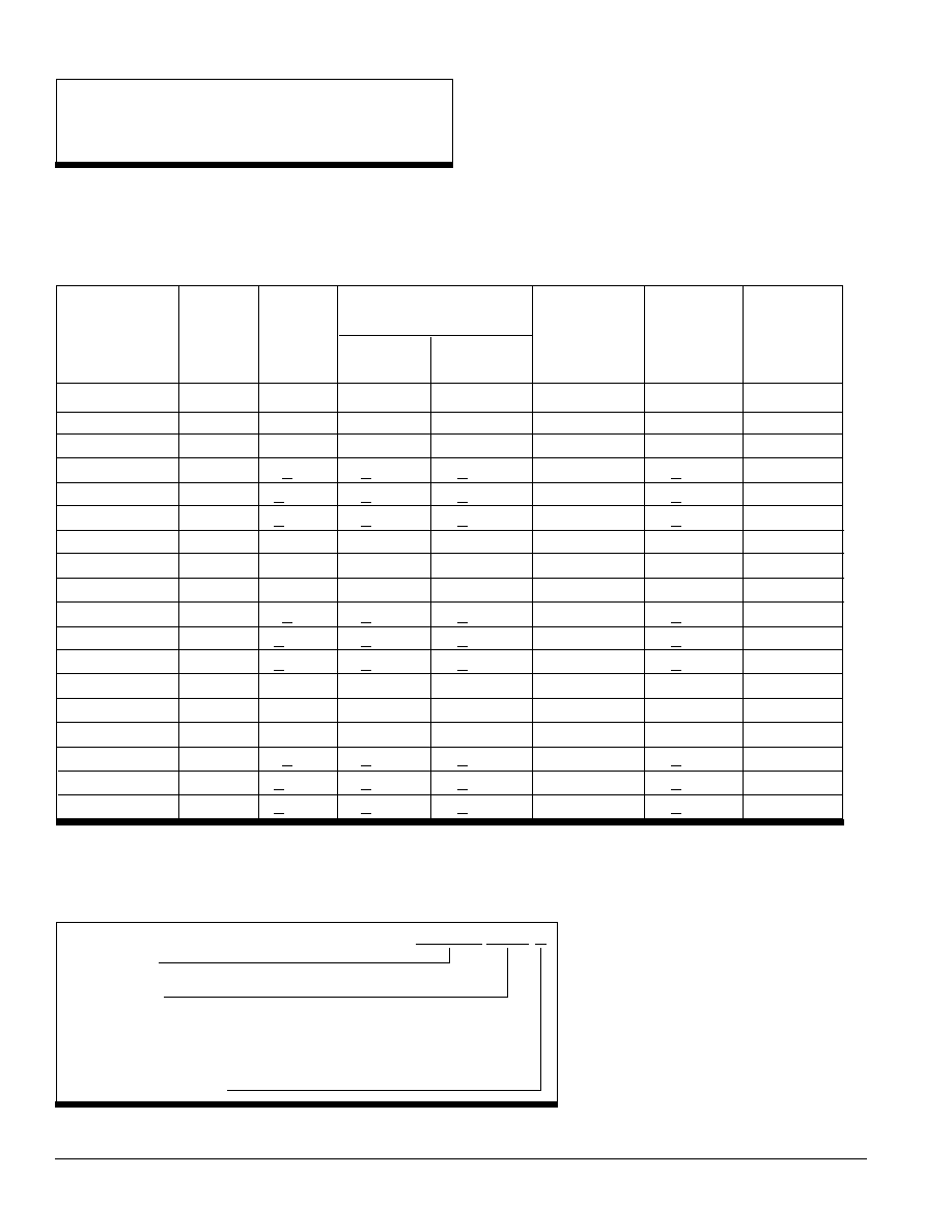
ELECTRICAL SPECIFICATIONS
Specifications typical at T
A
=25∞C, nominal input voltage, rated output current unless otherwise stated.
Nominal
Rated
Max Input
Max
Input
Output
Output Current (mA)
Current
Capacitive
Efficiency
Voltage
Voltage
(mA)
Load (
µµ
µµ
µ
F)
%
Model
(Volts)
(Volts)
Min Load Rated Load
Rated Load
(See Note 1)
WPC03R12S05
12
5.0
60
600
448
600
77
WPC03R12S12
12
12.0
24
250
445
250
80
WPC03R12S15
12
15.0
20
200
445
200
81
WPC03R12D05
12
+5.0
+30
+300
470
+300
74
WPC03R12D12
12
+12.0
+12
+125
475
+125
76
WPC03R12D15
12
+15.0
+10
+100
475
+100
77
WPC03R24S05
24
5.0
60
600
230
600
74
WPC03R24S12
24
12.0
24
250
230
250
75
WPC03R24S15
24
15.0
20
200
225
200
76
WPC03R24D05
24
+5.0
+30
+300
240
+300
73
WPC03R24D12
24
+12.0
+12
+125
235
+125
74
WPC03R24D15
24
+15.0
+10
+100
230
+100
75
WPC03R48S05
48
5.0
60
600
120
600
74
WPC03R48S12
48
12.0
24
250
118
250
75
WPC03R48S15
48
15.0
20
200
116
200
76
WPC03R48D05
48
+5.0
+30
+300
120
+300
75
WPC03R48D12
48
+12.0
+12
+125
118
+125
76
WPC03R48D15
48
+15.0
+10
+100
116
+100
77
NOTE 1:
Although minimum load specifications are indicated for load measurement purposes, all models will operate under no-load conditions.
WPC03R 2/99 REV A
Page 3
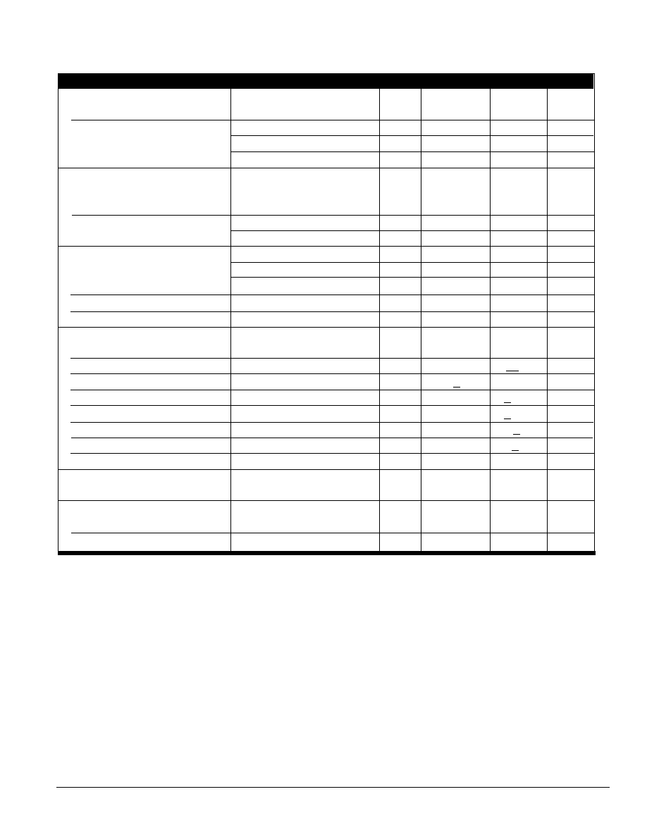
COMMON SPECIFICATIONS
Specifications typical at T
A
=25∞C, nominal input voltage, rated output current unless otherwise stated.
Parameter
Conditions
Min
Typ
Max
Units
Input
Voltage Range
9
12
18
Vdc
18
24
36
Vdc
34
48
72
Vdc
Reflected Ripple Current
50
mA p-p
Isolation
Safety Standards
Designed to meet requirements of
EN60950, EN41003 & UL1950
Rated Voltage
"L" Pinout
1500
Vdc
"E" Pinout
1000
Vdc
Test Voltage--60 Hz, 10 secs
"L" Pinout
1500
Vpk
"E" Pinout
1000
Vpk
Resistance
10
G
Capacitance
220
pF
Leakage Current
V
iso
=240Vac, 60 Hz
30
µ
Arms
Output
Rated Power
3
W
Voltage Setpoint Accuracy
+3.0
%
Temperature Coefficient
+0.02
%/∞C
Line Regulation-singles
Low line to high line
+1.5%
%
Line Regulation-duals
Low line to high line
+1.5%
%
Load Regulation-singles
Min load to rated load
+2%
%
Load Regulation-duals
Min load to rated load
+2%
%
Ripple & Noise
BW=5 Hz to 20 MHz
50
100
mV p-p
General
MTTF per MIL-HDBK-217, Rev F
T
A
=25∞
1,000,000
Hours
Temperature
Operation
-40
+85
∞C
Storage
-55
+125
∞C
WPC03R 2/99 REV A
Page 4
The information provided herein is believed to be reliable; however, C&D TECHNOLOGIES assumes no responsibility for inaccuracies or omissions. C&D TECHNOLOGIES assumes
no responsibility for the use of this information, and all use of such information shall be entirely at the user's own risk. Prices and specifications are subject to change without notice.
No patent rights or licenses to any of the circuits described herein are implied or granted to any third party. C&D TECHNOLOGIES does not authorize or warrant any C&D TECHNOLOGIES
product for use in life support devices/systems or in aircraft control applications.
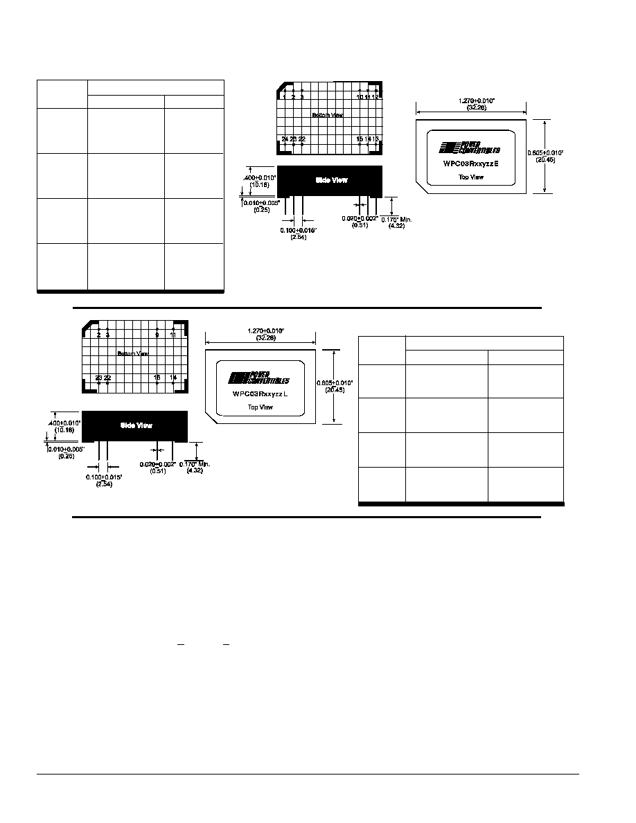
TECHNICAL INFORMATION
Notes:
1.
All dimensions in inches and (millimeters).
2.
Units are encapsulated with a low thermal resistance molding compound which has excellent chemical resis-
tance, wide operating temperature range and good electrical properties under high humidity environments. The
encapsulant and outer shell have UL94V-0 ratings. Lead material is brass with a solder plated surface to allow
ease of solderability.
3.
GRID: 0.100 inches, (2.54 mm).
4.
Pin Placement Tolerance: +0.015", (+.381 mm).
MECHANICAL SPECIFICATIONS
Pin
Pin Function
Number
Singles
Duals
2
-Vin
-Vin
3
-Vin
-Vin
9
No connection
Common
11
No connection
-Vout
14
+Vout
+Vout
16
-Vout
Common
22
+Vin
+Vin
23
+Vin
+Vin
PINOUT "E"
Pin
Pin Function
Number
Singles
Duals
1
+Vin
+Vin
2
No connection
-Vout
3
No connection
Common
10
-Vout
Common
11
+Vout
+Vout
12
-Vin
-Vin
13
-Vin
-Vin
14
+Vout
+Vout
15
-Vout
Common
22
No connection
Common
23
No connection
-Vout
24
+Vin
+Vin
PINOUT "L"